





PCB on PCB refers to a design where one printed circuit board is mounted, stacked, or electrically connected to another PCB. In practical electronics manufacturing, this structure is often called board-to-board PCB assembly, stacked PCB assembly, mezzanine PCB design, or PCB module integration. Engineers use it when one board cannot efficiently hold all functions, when a product needs replaceable modules, or when space is limited inside the enclosure.
This guide explains how PCB on PCB structures work, what interconnection methods are used, what design risks should be checked, and how manufacturers control quality during fabrication and assembly.
What Is PCB on PCB?
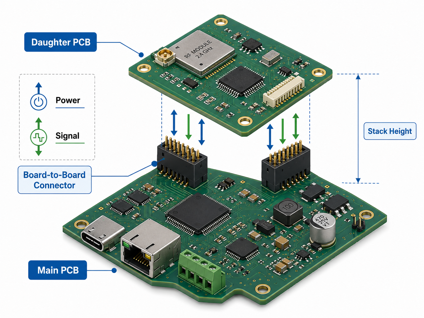
PCB on PCB is a construction method where two or more circuit boards are connected together through board-to-board connectors, pin headers, sockets, castellated holes, soldered pads, flex circuits, or custom interposers. One PCB may work as the main control board, while the second PCB may carry power, RF, sensors, displays, memory, communication modules, or daughter-card functions.
This design is common in compact electronic products because it allows engineers to separate circuit functions without expanding the main board area. For example, a product may use one base PCB for power and control, then place a smaller PCB above it for wireless communication or high-speed signal processing.
In manufacturing terms, PCB on PCB is not only a layout decision. It also affects connector selection, stack height, soldering process, mechanical tolerance, inspection access, repair strategy, and final functional testing.
Why Is PCB on PCB Important in Compact Electronics?
PCB on PCB is important because many modern electronic products require higher circuit density, modular design, and easier system upgrades. Instead of forcing every circuit into one crowded board, engineers can divide the system into several functional boards.
| Design Need | How PCB on PCB Helps |
|---|---|
| Limited enclosure space | Uses vertical space instead of increasing board length or width |
| Modular product architecture | Allows separate communication, sensor, display, or power modules |
| Faster design updates | One daughter board can be redesigned without changing the full system |
| Mixed technology integration | RF, analog, digital, and power circuits can be separated |
| Production flexibility | Different product versions can share the same main board |
For products such as industrial controllers, medical electronics, IoT devices, handheld instruments, automotive modules, and communication equipment, PCB on PCB design can reduce layout congestion and improve product scalability.
How Does PCB on PCB Work?
A PCB on PCB structure works by creating electrical and mechanical connection between two boards. The connection method depends on signal type, current level, stack height, product size, vibration environment, and production volume.
The most common structure uses a main PCB and a daughter PCB. The two boards are connected by mating board-to-board connectors, pin headers, sockets, or solderable edge contacts. Board-to-board connectors are widely used because they allow PCBs to be connected without wire harnesses and support compact product structures.
A reliable PCB on PCB design must control three points:
| Control Point | Engineering Requirement |
|---|---|
| Electrical path | Stable power, ground, signal, impedance, and current capacity |
| Mechanical alignment | Correct connector position, mating height, board spacing, and tolerance |
| Assembly process | Reflow compatibility, inspection access, test points, and final verification |
When these points are planned early, the stacked PCB assembly is easier to manufacture, inspect, and scale into production.
Main Types of PCB on PCB Structures
PCB on PCB structures can be designed in several ways. Each type has different benefits, cost levels, and assembly requirements.
| Type | Description | Common Use |
|---|---|---|
| Board-to-board connector stack | Two PCBs are connected by mating connectors | Industrial control, IoT, medical electronics |
| Pin header and socket stack | Simple vertical connection using through-hole or SMT headers | Prototypes, control modules, display boards |
| Mezzanine PCB | High-density board mounted above a main board | Communication devices, embedded systems |
| Castellated module | Small PCB soldered directly onto another PCB edge | Wireless modules, sensor modules |
| Flex-to-board connection | Flexible circuit links two rigid PCBs | Wearables, cameras, compact devices |
| Rigid-flex PCB alternative | Rigid and flexible sections are fabricated as one structure | High-reliability compact electronics |
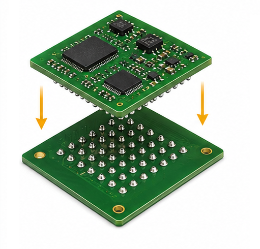
| Soldered board-on-board module | One small PCB is directly soldered to pads on the main PCB | RF modules, power modules, miniaturized devices |
For low-cost applications, pin headers may be enough. For compact and high-reliability electronics, fine-pitch board-to-board connectors or castellated modules are often preferred. For high-vibration products, mechanical support should be added through screws, spacers, staking, or enclosure locking features.
PCB on PCB vs Single PCB Design
A single PCB is often simpler to fabricate and assemble. PCB on PCB becomes valuable when the product requires modularity, vertical space usage, mixed circuit separation, or easier design iteration.
| Item | Single PCB | PCB on PCB |
|---|---|---|
| Board area | Larger footprint may be required | Uses vertical space efficiently |
| Assembly complexity | Usually simpler | Requires connector or module alignment |
| Design updates | Whole board may need revision | One module can be updated separately |
| Testing | One complete board test flow | Board-level and system-level testing needed |
| Cost | Lower for simple products | Higher if connectors and extra assembly are required |
| Repair or replacement | More difficult for single failed function | Module-level replacement may be possible |
| Signal control | Easier when routing is simple | Requires careful inter-board signal planning |
For early engineering samples, PCB on PCB can shorten development when different functional modules need independent verification. For high-volume production, it should be evaluated carefully because connectors, assembly fixtures, tolerance control, and testing all affect total cost.
Materials Used in PCB on PCB Manufacturing
The material selection depends on product environment, signal speed, heat, voltage, and mechanical stress.
| Material | Typical Use |
|---|---|
| FR4 | General control boards, power boards, communication modules |
| High-Tg FR4 | Products exposed to higher thermal stress |
| Rogers or other RF laminates | Antenna, RF, microwave, and high-frequency boards |
| Aluminum PCB | LED, power, and thermal management modules |
| Copper base PCB | High-power heat dissipation applications |
| Ceramic PCB | High thermal conductivity, high power, RF, and harsh environments |
| Flexible polyimide | Compact inter-board bending connection |
In PCB on PCB design, both boards do not always need the same material. A main board may use FR4, while a daughter board may use Rogers material for RF performance or ceramic substrate for thermal control. This mixed-material strategy can improve performance without forcing the whole system to use expensive materials.
Key Design Rules for PCB on PCB Layout
PCB on PCB layout should start with mechanical planning, not only circuit routing. The connector location, board spacing, enclosure clearance, and assembly sequence should be confirmed before final placement.
| Design Item | What to Check |
|---|---|
| Connector footprint | Match supplier land pattern and orientation |
| Stack height | Confirm board-to-board distance after mating |
| Board outline | Avoid enclosure interference and component collision |
| Keep-out area | Reserve space around connectors, screws, and tall components |
| Signal assignment | Place high-speed, power, ground, and low-speed pins logically |
| Ground return path | Provide enough ground pins near high-speed signals |
| Test access | Keep test points reachable after stacking |
| Thermal path | Avoid trapping heat between boards |
| Mechanical support | Add spacers, screws, or brackets for vibration-prone products |
| Assembly direction | Make sure the board can be soldered, inspected, and mated correctly |
For high-speed PCB on PCB designs, impedance control and return-path continuity are especially important. The PCB stack-up should define copper layers, dielectric thickness, material type, controlled impedance values, and ground reference planes before routing starts.
Board-to-Board Connectors for PCB on PCB Assembly
Board-to-board connectors are one of the most widely used solutions for PCB on PCB products. They support different orientations, spacing requirements, pin counts, and electrical needs. Some connector families are designed for high-speed signals, while others are optimized for power transfer, floating alignment, or compact stacking.
When choosing a connector, engineers should compare:
| Parameter | Selection Point |
|---|---|
| Pitch | Smaller pitch saves space but increases assembly difficulty |
| Stack height | Must match enclosure and component clearance |
| Current rating | Must support power rail requirements |
| Voltage rating | Must meet product safety and insulation needs |
| Mating cycles | Important for removable or serviceable modules |
| Alignment tolerance | Floating connectors help absorb small mechanical offsets |
| Contact plating | Gold plating improves contact reliability in many signal applications |
| SMT or through-hole | SMT saves space; through-hole improves mechanical strength |
| Signal speed | High-speed connectors need controlled impedance performance |
| Availability | Long-term supply and second-source risk should be reviewed |
A common mistake is selecting a connector only by pin count. In production, mating height, coplanarity, pick-and-place compatibility, reflow profile, and inspection method are just as important.
Manufacturing Process for PCB on PCB Products
PCB on PCB manufacturing normally involves both PCB fabrication and PCBA assembly. The exact process depends on whether the boards are detachable, soldered together, or assembled as a complete electronic module.
A typical process includes:
| Step | Process Detail |
|---|---|
| DFM review | Check board outline, connector footprint, solder mask, drill design, and assembly clearance |
| PCB fabrication | Produce each board according to stack-up, copper weight, surface finish, and tolerance requirements |
| Incoming inspection | Verify PCB dimensions, finish, solder mask, and electrical test status |
| SMT assembly | Place components and board-to-board connectors using stencil printing and reflow soldering |
| Through-hole assembly | Add pin headers, sockets, spacers, or mechanical supports when required |
| Board cleaning | Remove flux residue when the product requires high cleanliness |
| Sub-assembly test | Test each PCB before final stacking where possible |
| Final mating | Join boards using connectors, soldering, screws, or fixtures |
| Functional test | Verify full system performance after all boards are connected |
| Packing and traceability | Record batch data, inspection results, and shipment information |
IPC-A-610 provides acceptance requirements for electronic assemblies, while IPC-J-STD-001 covers requirements for soldered electrical and electronic assemblies. These standards are often referenced in PCB assembly quality control.
Testing Methods for PCB on PCB Assembly
Testing is critical because faults may appear at the board level, connector level, or full-system level. A PCB may pass electrical testing as a bare board, then fail after stacking because of connector alignment, solder joint defects, signal integrity problems, or mechanical stress.
| Test Method | Purpose |
|---|---|
| Bare board electrical test | Check open and short circuits before assembly |
| AOI | Inspect component placement, polarity, solder joints, and visible defects |
| X-ray inspection | Inspect hidden solder joints, BGA, QFN, and some connector solder areas |
| Flying probe test | Verify assembled circuits without expensive fixtures |
| ICT | Check component values, shorts, opens, and node-level faults |
| Functional test | Confirm product operation under real working conditions |
| Power-on test | Check current draw, voltage rails, and startup behavior |
| Connector mating test | Confirm stable electrical contact after board stacking |
| Thermal test | Check heat concentration between stacked boards |
| Vibration or drop test | Used when the product faces mechanical stress |
For high-reliability products, test planning should be done before layout completion. Test points must remain accessible after the boards are stacked. If the daughter board blocks key signals, the manufacturer may need custom fixtures, pogo-pin access, boundary scan, or staged testing.
Quality Standards and Compliance for PCB on PCB
PCB on PCB products may need different standards depending on the final application. For bare rigid printed boards, IPC-6012 covers qualification and performance requirements for rigid PCBs, including single-sided, double-sided, multilayer, blind or buried via, and metal core boards.
For visual acceptability of bare boards, IPC-A-600 describes target, acceptable, and nonconforming conditions that can be externally or internally observed on printed boards.
For environmental compliance, RoHS restricts hazardous substances in electrical and electronic equipment in the European Union. For safety-related PCB requirements, UL provides PCB testing and certification services against UL standards and other international, national, and regional requirements.
| Document | Why It Matters |
|---|---|
| Gerber files | Define copper, solder mask, silkscreen, and routing layers |
| Drill files | Define plated and non-plated holes |
| IPC-356 netlist | Helps verify electrical connectivity |
| BOM | Defines components, connectors, alternatives, and sourcing rules |
| Pick-and-place file | Supports automated SMT assembly |
| Assembly drawing | Shows component position, polarity, and stacking direction |
| Stack-up drawing | Defines material, copper, dielectric, and impedance structure |
| Test specification | Defines inspection and functional test requirements |
| Quality standard requirement | Clarifies IPC class, RoHS, UL, or customer-specific rules |
Common Failure Modes in PCB on PCB Designs
PCB on PCB failure often comes from mechanical, electrical, or process-related mismatch. Many issues can be prevented during DFM review.
| Failure Mode | Possible Cause | Prevention Method |
|---|---|---|
| Intermittent signal | Connector misalignment or weak contact | Use correct mating height, alignment posts, and mechanical support |
| Cracked solder joints | Board flexing, vibration, or heavy connector stress | Add screws, spacers, strain relief, or stronger connector type |
| Poor RF performance | Long return path or wrong connector assignment | Place ground pins near RF or high-speed signals |
| Overheating | Heat trapped between stacked boards | Add thermal vias, copper area, airflow gap, or heat sink path |
| Assembly collision | Tall components placed between boards | Run 3D mechanical clearance check |
| Solder bridging | Fine-pitch connector footprint or stencil issue | Optimize stencil aperture and solder paste volume |
| Hard-to-test board | Test points blocked after stacking | Add staged test points and fixture access early |
| Connector sourcing risk | Single-source connector selected | Check lifecycle, MOQ, lead time, and approved alternatives |
A strong engineering approach is to treat the connector area as both an electrical interface and a mechanical load point. This helps reduce field failures caused by repeated plugging, vibration, thermal cycling, or enclosure pressure.
Applications Using PCB on PCB
PCB on PCB structures are used in many electronic products where compact design, modularity, and multi-function integration are required.
| Application | Typical PCB on PCB Function |
|---|---|
| Industrial control | Main control board plus I/O, relay, or communication module |
| Medical electronics | Sensor board, display board, control board, or power module |
| Automotive electronics | LED driver module, radar board, control module, or interface board |
| IoT devices | Wireless module mounted on a base control PCB |
| Communication equipment | RF board stacked with digital processing board |
| Robotics | Motor control board connected to sensor or communication board |
| Consumer electronics | Display, camera, charging, or button module |
| Aerospace and UAV | Lightweight modular electronics with compact interconnects |
| Test instruments | Replaceable measurement boards and interface modules |
| LED lighting | Power driver board connected with control or thermal board |
For RF and high-speed applications, PCB on PCB design should be reviewed carefully because connector transition, grounding, impedance discontinuity, and board spacing can affect signal performance.
Case Study: Custom PCB on PCB Manufacturing for an Industrial Control Module
A customer needed a compact industrial control module with power regulation, signal processing, and communication functions inside a limited enclosure. A single PCB layout created routing congestion and made thermal separation difficult. The engineering solution was to use a PCB on PCB structure.
The lower board handled power input, protection circuits, and I/O terminals. The upper daughter board carried the microcontroller, communication interface, and signal conditioning circuits. Board-to-board connectors were selected based on stack height, current rating, and available mating tolerance.
During DFM review, the connector footprint was checked against the supplier datasheet. Tall capacitors were moved away from the stacking area. Test points were placed on the board edges so the assembly could be tested before and after final mating. Mechanical spacers were added to reduce connector stress during installation.
The production flow included PCB fabrication, SMT assembly, AOI inspection, sub-board testing, final board stacking, functional test, and packing with batch traceability. This approach reduced layout pressure, improved module organization, and made future product upgrades easier.
Cost Factors in PCB on PCB Manufacturing
PCB on PCB cost is affected by both PCB fabrication and assembly complexity. The cheapest structure is not always the most economical after testing, rework, and reliability risks are considered.
Main cost factors include:
| Cost Factor | Impact |
|---|---|
| Number of boards | More boards increase fabrication, assembly, and inspection steps |
| Connector type | Fine-pitch, high-speed, floating, or high-current connectors cost more |
| Stack height tolerance | Tight mechanical tolerance may require higher-grade connectors or fixtures |
| PCB material | RF, ceramic, aluminum, copper base, and high-Tg materials affect cost |
| Surface finish | ENIG is common for fine-pitch connectors and reliable contact areas |
| Assembly difficulty | Fine-pitch connectors, double-sided SMT, and hidden joints increase process control needs |
| Test fixture | Stacked products may require custom functional test fixtures |
| Production volume | Higher volume can reduce unit assembly cost after fixture investment |
| Quality requirements | IPC class, traceability, inspection depth, and documentation affect total cost |
| Component sourcing | Long lead-time connectors or single-source parts can increase procurement cost |
For cost control, engineers should confirm whether the product needs a detachable PCB module or a permanently soldered module. A removable connector improves serviceability but may cost more. A soldered castellated module can save height and connector cost, but it changes the repair and inspection strategy.
How to Choose a PCB on PCB Manufacturer
A reliable PCB on PCB manufacturer should understand both PCB fabrication and PCBA assembly. This matters because inter-board products require control across layout review, board tolerance, connector assembly, soldering, inspection, testing, and final system verification.
Before placing an order, check whether the manufacturer can provide:
| Capability | What to Confirm |
|---|---|
| DFM review | Connector footprint, stack height, solderability, test access, and mechanical clearance |
| PCB fabrication | Multilayer PCB, impedance control, HDI, RF PCB, MCPCB, ceramic PCB, or rigid-flex capability |
| PCBA assembly | SMT, through-hole, mixed assembly, fine-pitch connector placement, and reflow control |
| Component sourcing | Board-to-board connector availability, approved alternatives, and lifecycle checking |
| Testing | AOI, X-ray, electrical test, ICT, flying probe, and functional test |
| Quality system | IPC workmanship, RoHS support, traceability, and inspection records |
| Engineering support | BOM review, stack-up suggestions, assembly fixture advice, and failure analysis |
| Global delivery | Export packing, shipment coordination, and batch documentation |
For OEM and ODM projects, the manufacturer should also help evaluate whether the PCB on PCB structure is the best solution compared with one larger PCB, rigid-flex PCB, cable connection, or integrated module design.
What Files Are Needed Before Quoting PCB on PCB?
A complete quotation package helps the manufacturer evaluate cost, process, and risk accurately.
Prepare these files before requesting a quote:
| File or Information | Requirement |
|---|---|
| Gerber files | Required for each PCB |
| Drill files | Include plated and non-plated hole information |
| BOM | Include manufacturer part number, quantity, tolerance, package, and alternatives |
| Pick-and-place file | Required for SMT assembly |
| Assembly drawing | Show connector direction, polarity, and board stacking relationship |
| Stack-up requirement | Include material, copper thickness, board thickness, and impedance |
| 3D model | Strongly recommended for stacked board clearance checking |
| Test plan | Define electrical, functional, and environmental test requirements |
| Annual volume | Helps select suitable process and sourcing strategy |
| Compliance requirement | RoHS, UL, IPC class, medical, automotive, aerospace, or customer-specific rules |
For connector-based designs, the connector datasheet should also be provided. The mating pair, stack height, orientation, and tolerance must be checked before production.
FAQs About PCB on PCB
Q1: What does PCB on PCB mean?
PCB on PCB means one printed circuit board is mounted, stacked, soldered, or connected to another PCB. It is often used for daughter boards, communication modules, sensor modules, RF modules, display boards, and compact electronic assemblies. The purpose is usually to save space, separate functions, or make the product easier to upgrade.
Q2: Is PCB on PCB the same as board-to-board PCB assembly?
They are closely related. Board-to-board PCB assembly is one common form of PCB on PCB design. It usually uses connectors, headers, sockets, or direct soldering to connect two PCBs. PCB on PCB is a broader phrase because it can also include castellated modules, mezzanine boards, flex-linked boards, or soldered PCB modules.
Q3: What connector is best for PCB on PCB design?
The best connector depends on pitch, stack height, current rating, signal speed, vibration level, and mating cycle requirement. For simple control boards, pin headers may be enough. For compact industrial or medical devices, fine-pitch board-to-board connectors are often better. For vibration environments, floating or mechanically reinforced connectors are worth reviewing.
Q4: Can PCB on PCB be used for high-speed signals?
Yes, but the layout must control impedance, grounding, connector transition, and return path. High-speed signals should be assigned near ground pins, and the connector should support the required data rate. The PCB stack-up, connector datasheet, and signal integrity requirements should be reviewed together before layout approval.
Q5: Can one PCB be soldered directly onto another PCB?
Yes. A small module can be soldered directly onto a main board through castellated holes, edge pads, or solderable terminals. This method saves connector height and cost, but it makes rework more difficult. It is commonly used for wireless modules, compact sensors, and small functional modules.
Q6: Is PCB on PCB better than using cables?
PCB on PCB is often better when the product needs compact size, stable alignment, and reduced wire harness complexity. Cables are still useful when boards need flexible movement or longer spacing. The better option depends on enclosure design, vibration, assembly process, signal type, and maintenance needs.
Q7: What is the biggest risk in PCB on PCB assembly?
The biggest risk is usually poor coordination between mechanical design, connector selection, and assembly process. If stack height, component clearance, and connector tolerance are not checked early, the boards may collide, misalign, or create unstable contact. A 3D model and DFM review can prevent most of these problems.
Q8: Which surface finish is suitable for PCB on PCB?
ENIG is commonly used for fine-pitch assembly, flat soldering surfaces, and contact reliability. HASL may be acceptable for some low-cost boards, but it is less ideal for fine-pitch connector pads because of surface unevenness. The final choice depends on connector pitch, soldering process, cost target, and product reliability level.
Q9: How should PCB on PCB products be tested?
Testing should be done in stages. Each bare PCB should receive electrical testing first. After SMT assembly, AOI, X-ray, flying probe, or ICT may be used. After final stacking, functional testing should verify power, signal communication, connector contact, current draw, and product behavior under normal operating conditions.
Q10: Does PCB on PCB increase manufacturing cost?
It can increase cost because there are multiple boards, connectors, assembly steps, and test requirements. However, it may reduce redesign cost, enclosure size, wiring labor, and future upgrade cost. For modular products, the overall project cost may be better than forcing all functions into one complex PCB.
Q11: What spacing is needed between two stacked PCBs?
The spacing depends on connector height, tallest components, insulation clearance, airflow, and enclosure requirements. Engineers should check the connector mated height, component maximum height, solder joint profile, and manufacturing tolerance. A 3D clearance review is recommended before ordering prototypes.
Q12: Can PCB on PCB be used in automotive or medical electronics?
Yes. It can be used in automotive, medical, industrial, aerospace, and communication products when design, material, process, and testing requirements are properly controlled. For regulated industries, documentation, traceability, inspection standards, reliability testing, and supplier qualification become more important than in simple consumer products.
Conclusion
PCB on PCB design is a practical solution for compact, modular, and function-rich electronic products. It allows engineers to divide circuits into main boards and daughter boards, reduce layout congestion, and support different materials or technologies inside one product. The best result depends on early connector selection, stack-height planning, signal integrity review, test access, and manufacturing process control.
For selection, start with product structure and signal requirements. Then compare board-to-board connectors, soldered modules, flex connections, and rigid-flex alternatives. For purchasing, provide complete Gerber files, BOM, assembly drawings, stack-up data, connector datasheets, and test requirements so the manufacturer can review cost and production risk accurately.
If you are looking for reliable OEM manufacturing, ODM production, sample development, mass production, or custom engineering solutions, contact our engineering team for technical support and quotation service.
You may also like



Tags: PCB on PCB