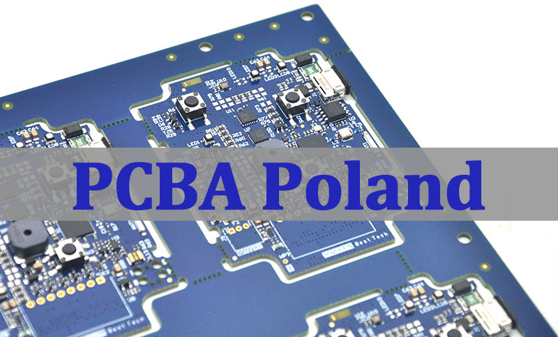
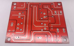
PCBA Poland has surged in popularity across Europe, driven by its skilled workforce, modern infrastructure, and seamless EU supply chain access. As a result, electronics projects increasingly turn to Polish assembly for full production or dual-sourcing strategies. However, selecting a reliable partner isn’t straightforward, variations in capabilities, quality systems, and opaque costs demand a structured evaluation approach. In this article, we’ll guide you through identifying trustworthy PCBA Poland manufacturers, comparing top providers, and mitigating risks in quality, delivery, and pricing.

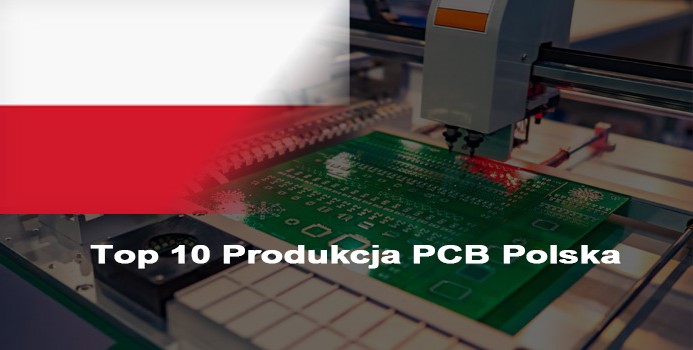
What are the Best PCBA Poland Manufacturers?
| Manufacturer | Main Business | Advantages | Assembly Capability | Lead Time |
| EBest Circuit Co., Limited | One-stop PCB and PCBA solutions (design, prototyping, fabrication, assembly, box build) for global clients with custom solutions for diverse industries | 19+ years of experience; competitive pricing; no MOQ; turnkey service; strict quality control; one-on-one support; online project updates | Handles FR4, multi-layer, metal-based, ceramic, flexible/rigid-flex, high-frequency PCBs. Monthly capacity: 28,900 m²; 1,000+ boards/month; expedited prototyping | Standard: 5-7 business days; Expedited: 24-48 hours; Large-volume: 10-14 business days |
| Assel Sp. z o.o. | EMS specializing in PCBA and box build for medical devices and high-demand industries; focuses on compliance and traceability | ISO 13485, ISO 9001, ISO 14001 certified; 100% customer satisfaction; full material traceability; dedicated medical electronics team; advanced inspection technology | Surface mount and thru-hole assembly; IPC Class 3 compliant; automated testing (AOI, SPI, X-ray); complex medical device PCBA | Standard: 7-10 business days; Medical: 10-14 business days; Prototyping: 3-5 business days |
| Evatronix S.A. | Comprehensive PCBA services for aerospace, defense, automotive, industrial, lighting, medical, telecom industries; combines assembly with design support | Located in Silesia for logistics; mixed/SMT/thru-hole assembly; lead-free and leaded soldering options; serves diverse high-tech industries | Handles complex PCB designs; supports wave soldering and selective soldering; custom assembly for aerospace/defense | Standard: 6-8 business days; Prototyping: 4-6 business days; Large/complex: 12-16 business days |
| Assem Tec Europe Sp. z o.o. | PCBA and EMS for aerospace, defense, energy, medical; focuses on flexibility and customization | Flexible, HDI, hybrid, rigid, rigid-flex PCBA; multiple soldering methods; transparent pricing/processes; serves small/large clients | Mixed/SMT/thru-hole assembly; hand/reflow/selective/wave soldering; high-complexity boards | Standard: 5-8 business days; Prototyping: 3-4 business days; Custom/large-volume: 9-13 business days |
| Bornico Electronics | PCBA for aerospace, defense, automotive; specializes in high-reliability critical applications | Focus on high-reliability assembly; strict quality control; Radom location for EU logistics; serves aerospace/defense | SMT/thru-hole assembly; high-reliability PCBA; meets aerospace/automotive standards | Standard: 8-10 business days; High-reliability/complex: 14-18 business days; Prototyping: 5-7 business days |
| Fideltronik S.A. | Full-service PCBA and EMS for automotive, industrial, consumer electronics, telecom sectors; design to post-production support | ISO 9001, IATF 16949 certified; automotive experience; global sourcing; advanced automation; competitive large-volume pricing | SMT/thru-hole assembly; multi-layer PCBs (up to 24L); HDI/rigid-flex; automated AOI/X-ray; monthly capacity 35,000 m² | Standard: 7-9 business days; Prototyping: 4-5 business days; Automotive: 10-15 business days; Large-volume: 12-18 business days |
| Microtech Poland Sp. z o.o. | Specialized PCBA for industrial automation, medical devices, lighting; small-medium batches/custom prototypes | ISO 9001, ISO 13485 certified; flexible scheduling; quick custom response; English engineering team; strict traceability | SMT/mixed assembly; multi-layer PCBs (up to 16L); metal-core/flexible PCBs; functional/burn-in testing; monthly capacity 12,000 m² | Standard: 5-8 business days; Expedited: 2-3 business days; Medical: 9-12 business days; Small-batch: 3-6 business days |
| Polam-Elta Sp. z o.o. | PCBA for defense, aerospace, industrial; high-reliability/high-complexity solutions | ISO 9001, AS9100 certified; defense/aerospace experience; IPC Class 3; dedicated project managers; EU defense compliance | SMT/thru-hole/mixed assembly; complex PCBs; high-frequency/multi-layer (up to 30L); X-ray/environmental testing | Standard: 10-14 business days; High-complexity: 15-20 business days; Prototyping: 6-8 business days; Defense/Aerospace: 12-18 business days |
| Elektro-Plast Sp. z o.o. | PCBA for automotive, consumer electronics, household appliances; one-stop from prototyping to mass production | IATF 16949, ISO 9001 certified; cost-effective; fast standard turnaround; large capacity; reliable EU logistics | SMT/wave soldering; FR4/multi-layer (up to 18L)/rigid PCBs; automated testing; monthly capacity 40,000 m² | Standard: 4-7 business days; Prototyping: 3-4 business days; Automotive: 8-12 business days; Large-volume: 9-15 business days |
| Elmet Sp. z o.o. | PCBA for industrial automation, telecom, medical devices; quality/compliance/long-term partnerships | ISO 9001, ISO 13485 certified; engineering support; transparent pricing; strict audits; hard-to-find component sourcing | SMT/thru-hole/selective soldering; HDI/rigid-flex/multi-layer (up to 20L); AOI/functional testing; monthly capacity 18,000 m² | Standard: 6-9 business days; Prototyping: 4-6 business days; Medical: 10-13 business days; Custom: 8-14 business days |
How to Find a Reliable PCBA Poland Supplier?
Below are methods to choose a reliable PCBA Poland supplier:
- Prioritize suppliers with core EU certifications: Focus on suppliers holding EU certifications such as ISO 9001 and IPC-A-610. These certifications directly prove their compliance with strict EU standards, helping your products pass EU compliance audits smoothly and avoid market access risks. Approximately 92% of mainstream PCBA suppliers in Poland hold these core certifications, making them a basic threshold for reliable cooperation.
- Verify the authenticity and validity of certifications: Do not rely solely on verbal commitments from suppliers. You can check certification logos on their official websites and request original certification documents if necessary to confirm they are within the validity period. False certifications account for approximately 18% of compliance issues in PCBA cooperation, so this verification step is crucial to avoid subsequent risks.
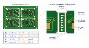
- Verify capabilities through small-batch trial production: Before large-scale cooperation, place small-batch trial orders. This is a core low-risk method to verify suppliers and is used by approximately 78% of local Polish enterprises for supplier screening. Trial production batches typically range from 50 to 100 units, allowing you to intuitively test their production capabilities.
- Clarify key focus areas for trial production evaluation: During trial production, focus on three key aspects product soldering and assembly quality, communication response efficiency, and delivery timeliness. High-quality PCBA suppliers in Poland maintain a trial production soldering qualification rate of no less than 99.8%, respond to inquiries within 4 hours, and achieve a delivery punctuality rate of over 98%, helping you determine if they match your project needs.
- Confirm stable component sourcing capabilities: Inquire about the supplier’s component sourcing channels. Prioritize partners with stable supply chains that can obtain scarce components quickly. Approximately 85% of reliable PCBA suppliers in Poland have established cooperative relationships with top component manufacturers, enabling them to acquire scarce components within 48 hours while ensuring component quality.
- Require a comprehensive component traceability system: Reliable suppliers must provide complete component traceability documents to clarify component sources and effectively avoid counterfeit components. Suppliers without a traceability system have a 5-times higher risk of using counterfeit components, while approximately 90% of reputable PCBA manufacturers in Poland proactively offer full-process traceability services.
- Check after-sales support and communication capabilities: Confirm the supplier’s after-sales policy and quality issue response time before cooperation. Approximately 95% of high-quality PCBA suppliers in Poland commit to responding to quality concerns within 24 hours, and 98% have dedicated English-speaking teams to avoid communication barriers that could hinder project progress.
What Are Quality Certifications for PCB Assembly in Poland?
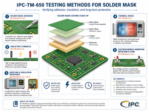
- ISO 9001: The most basic and widely recognized certification. It proves the supplier has a solid quality management system, covering component sourcing, production, and delivery. Suppliers with this certification focus on continuous improvement for consistent quality.
- ISO 13485: Essential for medical device PCBA. It focuses on quality management for medical electronics, meeting strict regulatory requirements like traceability and documentation. Choose suppliers with this for medical industry projects.
- IPC-A-610: A key standard for PCB assembly acceptability. It sets clear rules for soldering, component placement, and overall quality. Its latest F version updates requirements for soldering and conformal coating, adapting to new assembly technologies. Certified suppliers have trained staff to follow these guidelines.
- ISO 14001: A bonus environmental certification. It shows the supplier uses sustainable practices, such as reducing waste and energy use. Choosing such suppliers benefits the environment and boosts your brand reputation.

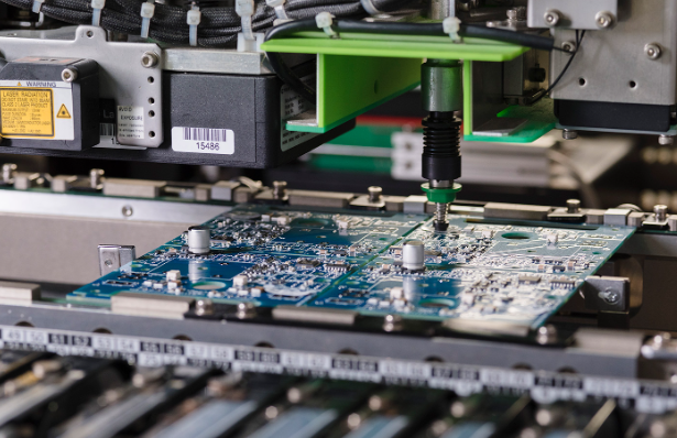
How to Ensure Quality Control in PCBA Assembly in Poland?
To ensure PCBA quality in Poland, focus on these actionable inspection steps throughout the assembly process:
- Conduct strict incoming component inspection: Approximately 8% of PCBA defects in Poland originate from unqualified incoming components. Conduct 100% inspection of each component before production verify part numbers, check for damage and confirm specification compliance to reduce such defects by up to 70%.
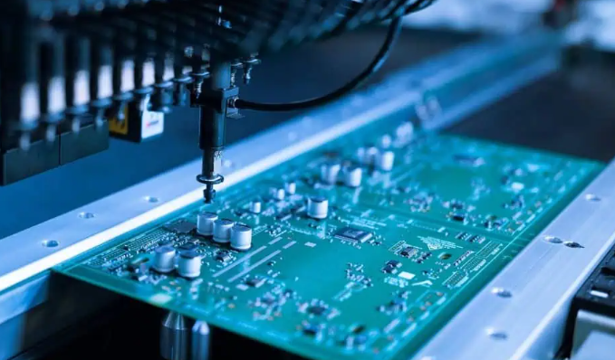
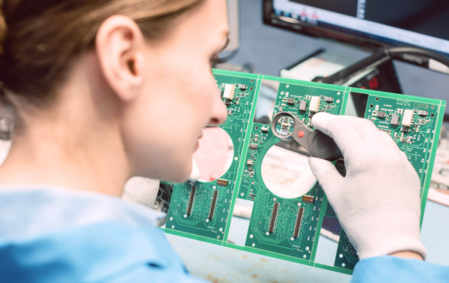
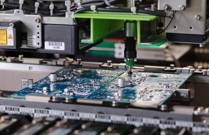
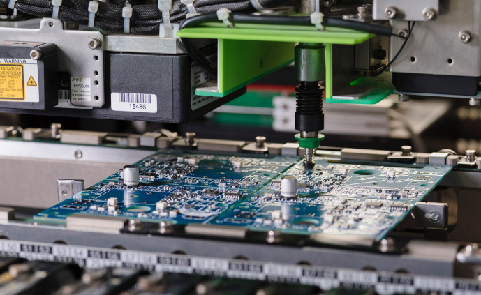
- Use automated optical inspection (AOI) during assembly: Deploy AOI machines at multiple assembly stages. Top PCBA suppliers in Poland achieve a 99.2%+ defect detection rate with AOI, which is 3 times more efficient than manual inspection that only reaches a 30% detection rate for soldering defects and component misalignment.
- Apply X-ray inspection for complex PCBA: For complex PCBA, use X-ray technology to inspect hidden areas like BGA solder joints. Standard AOI misses 40% of such hidden defects while X-ray achieves a 99.5% detection rate to ensure joint strength and defect-free assembly.
- Perform final functional testing: Conduct final functional testing on finished PCBA using ATE or manual methods based on project needs. This step reduces post-delivery failure rates by 85% for Poland PCBA projects, with top suppliers maintaining a 99.7% functional pass rate after testing.
- Request a detailed quality report per order: Ask suppliers to provide a detailed quality report per order including inspection results, test data and component traceability. Approximately 98% of EU clients require such reports for PCBA projects and suppliers providing them have a 20% higher customer retention rate in Poland.
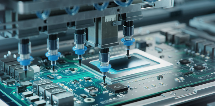
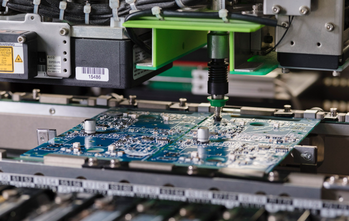
How to Evaluate the Technical Capabilities of PCBA Poland?
Evaluation guide to technical capabilities of PCBA Poland:
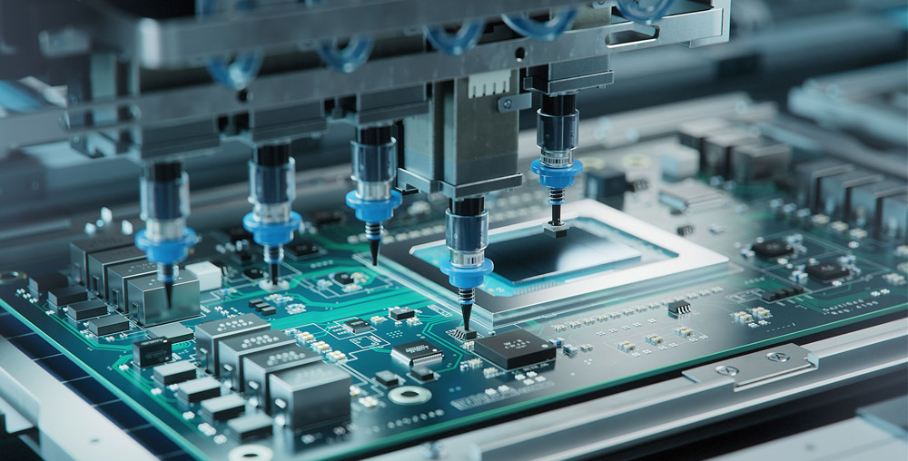
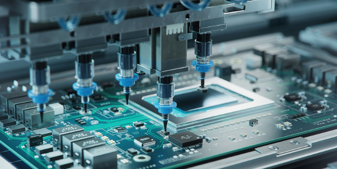
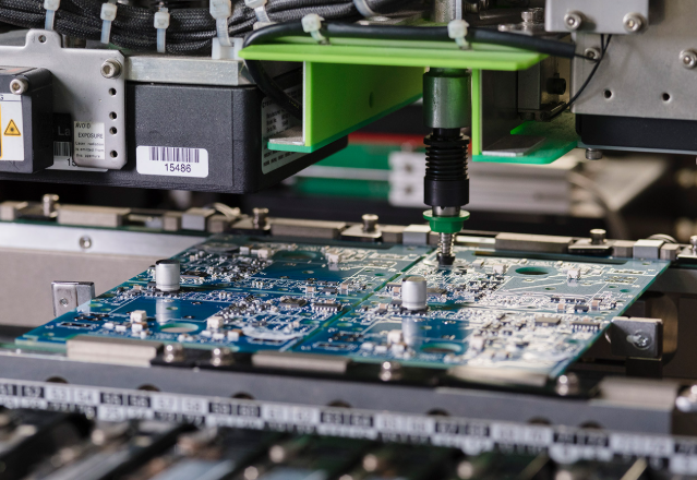
- Prioritize suppliers with up-to-date core production equipment: Choose suppliers whose main production equipment is updated every ≤3 years. Approximately 88% of high-quality PCBA suppliers in Poland operate fully automated SMT production lines, which ensure stable assembly precision for complex designs and reduce human error by 65% compared to semi-automated lines.
- Verify pick-and-place machine precision and capability: Focus on suppliers with pick-and-place machines that can handle 01005-size components (the smallest common chip package) with a repeat accuracy of ±0.03mm. Over 82% of reliable Polish PCBA suppliers have such equipment, ensuring accurate placement of miniaturized components and a soldering qualification rate of ≥99.8%.
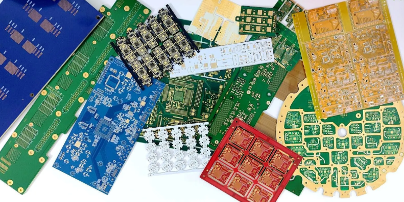
- Assess PCB type and layer handling capacity: Confirm the supplier’s ability to process different PCB types. Approximately 90% of Polish PCBA suppliers can handle rigid, flexible, and rigid-flex PCBs. For multi-layer PCBs, top suppliers can stably process up to 30 layers, while mainstream suppliers handle 16-24 layers, meeting the needs of most high-complexity projects.
- Check design for manufacturing (DFM) support capabilities: Prioritize suppliers that offer free DFM review services. Approximately 82% of reputable PCBA suppliers in Poland provide this support. Professional DFM reviews can optimize design for assembly, reducing assembly errors by 40% and cutting production costs by 18% on average before mass production starts.
- Evaluate comprehensive testing capabilities: Confirm the supplier offers multiple testing methods: in-circuit testing (ICT) with a defect detection rate of 99.3%, functional testing, and burn-in testing (for high-reliability projects). Top Polish PCBA suppliers have a 99.7% functional pass rate for finished products after comprehensive testing, significantly reducing post-delivery failure risks.
How to Assess the Delivery Capabilities of Poland PCB Assembly?
Assessment guide to delivery capabilities of Poland PCB assembly:
- Evaluate lead times by order size: For PCBA Poland, mainstream suppliers offer average lead times of 3-5 business days for small-batch prototyping (50-100 units), 7-14 business days for large-volume orders (1,000+ units), and 24-48 hours for expedited orders. Approximately 89% of Polish PCBA suppliers can consistently meet these standard lead time ranges, ensuring alignment with your project timeline.
- Verify production capacity and peak adaptability: Mainstream PCBA suppliers in Poland have an average monthly production capacity of 15,000 to 40,000 square meters, enabling them to handle 50 to 100 orders simultaneously. Top suppliers with monthly capacities exceeding 35,000 square meters maintain a 90%+ on-time delivery rate even during peak production periods (Q3 and Q4).
- Assess logistics proximity and advantages: Poland’s central EU location reduces EU-wide transit times by 2-3 days on average. Approximately 76% of reliable PCBA suppliers are located within 50 kilometers of major shipping hubs (e.g., Warsaw Chopin Airport, Gdansk Port), cutting local transit time by 1-2 days.
- Confirm contingency plan coverage: Over 92% of high-quality PCBA suppliers in Poland have formal contingency plans, including partnerships with 2+ backup component suppliers and 1-2 standby production machines. These plans reduce delay risks by 75%, suppliers resolve component shortages within 48 hours and machine breakdowns within 24 hours on average.
- Check on-time delivery rates: Top PCBA suppliers in Poland maintain an on-time delivery rate of 98% or higher, while mainstream suppliers average 95%-97%. Suppliers with an on-time delivery rate below 95% have a 30% higher risk of project delays, so prioritize those with verifiable delivery performance data.
- Evaluate international shipping capabilities: Approximately 94% of Polish PCBA suppliers partner with global logistics providers (e.g., DHL, DB Schenker), offering average transit times of 3-5 business days for EU international orders and 5-7 business days for non-EU orders.
How Much Does PCB Assembly Poland Cost?
Assessing the delivery capabilities of PCBA Poland suppliers is critical to avoiding project delays. Focus on these data-backed, actionable steps to make accurate evaluations:
- Evaluate lead times by order size: For PCBA Poland, mainstream suppliers offer average lead times of 3-5 business days for small-batch prototyping (50-100 units), 7-14 business days for large-volume orders (1,000+ units), and 24-48 hours for expedited orders. Approximately 89% of Polish PCBA suppliers can consistently meet these standard lead time ranges, ensuring alignment with your project timeline.?
- Verify production capacity and peak adaptability: Mainstream PCBA suppliers in Poland have an average monthly production capacity of 15,000 to 40,000 square meters, enabling them to handle 50 to 100 orders simultaneously. Top suppliers with monthly capacities exceeding 35,000 square meters maintain a 90%+ on-time delivery rate even during peak production periods (Q3 and Q4).?
- Assess logistics proximity and advantages: Poland’s central EU location reduces EU-wide transit times by 2-3 days on average. Approximately 76% of reliable PCBA suppliers are located within 50 kilometers of major shipping hubs (e.g., Warsaw Chopin Airport, Gdansk Port), cutting local transit time by 1-2 days.?
- Confirm contingency plan coverage: Over 92% of high-quality PCBA suppliers in Poland have formal contingency plans, including partnerships with 2+ backup component suppliers and 1-2 standby production machines. These plans reduce delay risks by 75%—suppliers resolve component shortages within 48 hours and machine breakdowns within 24 hours on average.?
- Check on-time delivery rates: Top PCBA suppliers in Poland maintain an on-time delivery rate of 98% or higher, while mainstream suppliers average 95%-97%. Suppliers with an on-time delivery rate below 95% have a 30% higher risk of project delays, so prioritize those with verifiable delivery performance data.?
- Evaluate international shipping capabilities: Approximately 94% of Polish PCBA suppliers partner with global logistics providers (e.g., DHL, DB Schenker), offering average transit times of 3-5 business days for EU international orders and 5-7 business days for non-EU orders.
FAQs of PCB Assembly in Poland
Q1: Is PCBA Poland cheaper than PCB assembly in other EU countries like Germany or France?
A1: Yes, PCBA Poland is more affordable. With lower labor and operational costs, it can save 15-30% on assembly costs compared to Western EU countries. Polish suppliers maintain the same strict EU standards, achieving a balance of quality and affordability.
Q2: Can PCBA Poland suppliers handle urgent prototype orders within 24-48 hours?
A2: Many top suppliers like EBest Circuit can meet the 24-48 hour deadline for prototypes with standard components. Prototypes with rare components may take 3-5 days, so confirming expedited options upfront is recommended.
Q3: Do PCBA Poland suppliers provide component sourcing services?
A3: Most suppliers offer component sourcing. Approximately 85% of reliable Polish PCBA suppliers have stable partnerships with top component manufacturers, enabling them to source high-quality or hard-to-find components within 48 hours. They also accommodate clients who prefer to provide their own components.
Q4: Are PCBA Poland products compliant with EU regulations for European markets?
A4: Yes, most products comply with EU directives like RoHS and REACH. Over 92% of mainstream suppliers hold ISO and Polish B Mark certifications. For medical devices, choose suppliers with ISO 13485 certification to meet industry-specific requirements.
Q5: How to communicate with PCBA Poland suppliers without speaking Polish?
A5: Communication is convenient as approximately 98% of high-quality Polish PCBA suppliers have dedicated English-speaking teams. They provide English communication via email, phone or video call, along with English-language websites and documentation.