PCB manufacturing PCB manufacturing
Home > Blog

Fast PCB Prototype Australia with Free DFM

February 17th, 2026

When seeking reliable prototyping services in the region, PCB prototype Australia stands as a critical link in electronic project advancement, with demands focusing on speed, precision and quality. Our PCB prototype Australia services are tailored to address the unique challenges of the local market, combining proven expertise and efficient delivery to support seamless project progression without unnecessary delays or compromises.

PCB Prototype Australia, https://www.bestpcbs.com/blog/2026/01/pcb-prototype-australia/

Top 10 PCB Factories for Prototype

Company NameAdvantagesPrototyping CapabilityPrototyping Lead Time
EBest Circuit Co., Limited19-year industry experience, multiple quality certifications, MES system for production tracking1-30 layers, HDI PCB, ceramic PCB, line width/spacing ≤40μm, impedance control ±3%Regular: 48-72 hours; Express: 24 hours
Alfatron Pty LtdAustralian-owned family business since 1978, high confidentiality, rich testing capabilities1-12 layers, rigid-flex PCB, HDI, automated assembly and AOI/ICT testingRegular: 3-5 days; Express: 48 hours
Allegro Services30+ years of local experience, full-process PCBA services, professional technical team1-60 layers, rigid PCB, SMT double-sided mounting, laser-guided assemblyRegular: 4-6 days; Express: 72 hours
4 Volts Electronic Engineering MelbourneLocal Melbourne-based, fast response, suitable for small-batch prototypes1-8 layers, rigid PCB, FR-4 material, basic electrical testingRegular: 5-7 days; Express: 48 hours
Artronic Australia Pty. LtdCost-effective, flexible order terms, good after-sales service1-10 layers, rigid PCB, standard FR-4, surface treatment options (immersion gold, HAL)Regular: 6-8 days; Express: 72 hours
B.E.C. Manufacturing Pty LtdSpecializes in flexible and rigid PCB, diverse material options1-10 layers, flexible/rigid PCB, copper/FR-4/Teflon materialsRegular: 4-7 days; Express: 5 days
Broad Avenue Industries Pty LtdISO 9001 certified, supports HDI and hybrid PCB, UL certified1-10 layers, HDI, hybrid PCB, aluminum/copper substratesRegular: 3-6 days; Express: 48 hours
Circuitwise AustraliaFocus on medical and aerospace PCB, strict quality control, compliance with international standards1-16 layers, HDI, ceramic PCB, medical-grade material and testingRegular: 5-8 days; Express: 72 hours
PCB Solutions AustraliaOnline quoting system, fast file review, transparent production process1-12 layers, rigid PCB, impedance control, basic AOI testingRegular: 4-6 days; Express: 48 hours
Melbourne PCB Co.Local production, short delivery distance, customized prototype solutions1-8 layers, rigid PCB, FR-4 halogen-free, small-size prototype support (6*6mm)Regular: 5-7 days; Express: 72 hours

Pain Points of Australia Prototype PCB

  • Is it hard to find PCB prototype Australia services that offer 24-hour express delivery for urgent projects?​
  • Does PCB prototype Australia often have high costs for small-batch or complex prototypes like HDI boards?​
  • Can most PCB prototype Australia providers meet the strict quality requirements of medical electronic products?​
  • Is it difficult to track the real-time production progress of PCB prototype Australia orders?​
  • Do many PCB prototype Australia factories lack the capability to produce special substrates like ceramic PCB?​
  • Is the minimum order quantity of most PCB prototype Australia services too restrictive for small-scale experiments?​
  • Do PCB prototype Australia providers often have long lead times for complex multi-layer (16+ layers) prototypes?

Why Choose EBest(Best Technology) for PCB Prototype Australia?

Reasons Why Choose EBest( Best Technology) for PCB Prototype Australia:

  • Expedited Service: We offer 24-hour fast prototyping and delivery, solving the urgent project needs that many providers cannot meet.
  • Rich Experience: 19 years of PCB production experience, serving 5000+ global clients, with mature technology to reduce production costs and our small-batch prototype prices are 15% lower than the local Australian average.
  • Strong Process Capability: We specialize in HDI PCB (line width/spacing ≤30μm) and ceramic PCB (alumina/aluminum nitride substrates), covering the special substrate needs that many factories lack.
  • Strict Quality Control: Certified by ISO9001, AS9100D, and IATF 16949, with 3 rounds of testing (AOI, X-ray, electrical testing) to ensure a prototype qualification rate of 99.8%.
  • Free DFM Service: We provide free Design for Manufacturability (DFM) reviews to identify potential design issues in advance, helping avoid production delays, rework costs and ensure smooth manufacturing processes.
  • Full-Service Support: We provide one-stop PCBA services, integrating prototype, assembly, and testing, saving time and costs for clients.
  • Transparent Production: Equipped with MES production management system, all production data is traceable, allowing real-time query of order progress.
  • Flexible MOQ: Minimum order quantity of 1 piece, fully adapting to small-scale experiment needs, solving the MOQ restriction problem of most services.
Why Choose EBest(Best Technology) for PCB Prototype Australia, https://www.bestpcbs.com/blog/2026/01/pcb-prototype-australia/

Types of PCB Prototype Australia We Can Offer

  • Rigid PCB Prototype: 1-30 layers, FR-4, FR-4 halogen-free, high Tg materials, suitable for most electronic products.
  • HDI PCB Prototype: 2-20 layers, blind/buried vias, line width/spacing ≤30μm, for high-density electronic devices.
  • Ceramic PCB Prototype: Alumina (24-28 W/mK) and aluminum nitride (170-230 W/mK) substrates, for high-temperature and high-power scenarios.
  • Flexible & Rigid-Flex PCB Prototype: 1-12 layers, laser microvias, adaptable to small or irregular installation spaces.
  • Metal Core PCB Prototype: Aluminum/copper substrates, thermal conductivity up to 380 W/mK, for LED and high-power electronic products.
  • Impedance Controlled PCB Prototype: Impedance tolerance ±3%, suitable for high-frequency signal transmission (insertion loss <0.3 dB/inch @28 GHz).

Quality Standards for PCB Prototype Australia

  • Raw Material Standard: All substrates (FR-4, ceramic, metal) comply with IPC standards, with 100% supplier qualification checks and batch testing to ensure consistency.​
  • Process Standard: Adhere strictly to ISO9001, AS9100D, and IATF 16949 certifications, using laser direct imaging (LDI) technology to guarantee process precision.​
  • Testing Standard: Conduct AOI inspection (±12μm accuracy), X-ray testing for blind/buried vias, 10V-250V electrical testing, and thermal stress simulation to eliminate defects.​
  • Impedance Standard: Maintain ±3% impedance control for high-frequency prototypes, with dynamic calibration throughout the design-to-production process.​
  • Surface Treatment Standard: Offer immersion gold (20-30μm), lead-free HAL, and chemical tin options, all fully compliant with RoHS standards.​
  • Dimensional Standard: Ensure board thickness tolerance ±0.1mm, minimum drilled hole size 0.25mm, and line width/spacing tolerance ±0.075mm.
Quality Standards for PCB Prototype Australia, https://www.bestpcbs.com/blog/2026/01/pcb-prototype-australia/

Lead Time for Prototype PCB Australia

LayersNormal ServiceFastest Service
17 Days24 H
28 Days24 H
410 Days48 H
610 Days72 H
812 Days72 H
≥10TBDTBD

Case Studies of Medical PCB Prototype Australia

Project Background

A Melbourne-based Australian medical device company specializes in the R&D and production of portable patient monitors. They needed a high-reliability PCB prototype for a new generation of monitors, which required strict compliance with medical industry standards and urgent delivery to meet their product launch schedule.

Project Requirements

  • Prototype Type: 8-layer HDI PCB, line width/spacing 40μm/40μm, impedance control ±5%.
  • Material: FR-4 halogen-free (high Tg 170℃), meeting medical biocompatibility standards.
  • Quality: Compliance with ISO 13485 and IPC Class 3, 100% electrical testing and AOI inspection.
  • Lead Time: Total delivery within 3 days (urgent project launch demand).

Project Challenges

  • Tight Lead Time: Most PCB prototype Australia providers require 4-6 days for 8-layer HDI prototypes, failing to meet the 3-day deadline.
  • Strict Quality: Medical-grade PCB requires zero defects, with higher testing standards than ordinary industrial prototypes.
  • Precision Requirements: HDI structure with tight line width/spacing and impedance control, requiring high-precision production equipment.

Our Solutions

  • Urgent Production Arrangement: Activated our 24-hour express production line, assigning 3 dedicated technicians to the project to shorten production time.
  • Quality Control Enhancement: Added a pre-production design review (DFM) to avoid design errors, and adopted dual AOI testing (pre and post-soldermask) to ensure zero defects.
  • Precision Process Control: Used laser direct imaging (LDI) technology and automated impedance testing to ensure the line width and impedance accuracy meet requirements.

Output Results

  • Delivery: Completed production and testing in 2.5 days, delivered 1 day ahead of the client’s deadline.
  • Yield Rate: 99.9% prototype qualification rate, with zero defects in electrical and visual testing.
  • Client Feedback: “The prototype quality exceeds our expectations, and the fast delivery helps us launch the new product on schedule. We will continue to cooperate with you for all our PCB prototype Australia needs.”
Case Studies of Medical PCB Prototype Australia, https://www.bestpcbs.com/blog/2026/01/pcb-prototype-australia/

FAQs of PCB Prototype Service Australia

Q1: How to solve the problem of long lead times for complex prototype orders?​
A1: We specialize in solving urgent prototype needs with our 24-hour express service for simple boards and 48-72 hours for complex multi-layer or HDI boards. Unlike ordinary providers, we optimize production processes and activate dedicated production lines exclusively for your orders, cutting lead times by 50% while maintaining strict quality control. Our efficient workflow ensures you get high-quality prototypes on time, every time.​
​
Q2: Can your prototype services meet the quality standards of medical equipment?​
A2: Absolutely. We hold strict certifications including ISO 13485, ISO 9001 and AS9100D, specifically tailored to meet the rigorous requirements of medical equipment production. We select only medical-grade raw materials and conduct triple testing (AOI, X-ray, electrical testing) to ensure zero defects. With a 99.8% medical PCB prototype qualification rate, we are the trusted choice for medical equipment-related prototype needs.​
​
Q3: What if I need a small batch (1-5 pieces) of ceramic PCB prototypes, which most factories do not support?​
A3: We excel at fulfilling small-batch prototype needs, with a minimum order quantity (MOQ) of 1 piece for all prototype types, including ceramic PCBs. We own specialized ceramic substrate production equipment and have rich experience in manufacturing ceramic prototypes, so you won’t incur extra costs for small orders. We eliminate the restrictions that most providers impose, making it easy for you to complete small-scale experiments or R&D projects.​
​
Q4: How can I track the real-time production progress of my prototype order?​
A4: We provide a dedicated, user-friendly order tracking system directly linked to our MES production management system. Once you place an order, you’ll receive a unique tracking link that lets you check every stage of production in real time from design review and manufacturing to testing and shipping. Data is updated every 2 hours, giving you full transparency and peace of mind, so you never have to wonder about your order’s status.​
​
Q5: How do you help avoid design errors that lead to production delays or rework?​
A5: We offer a free Design for Manufacturability (DFM) review service, an exclusive advantage that sets us apart from other providers. Our professional technical team will carefully review your design files in advance, identifying potential issues that could cause delays or rework. We provide detailed optimization suggestions to ensure your design is production-ready, saving you time, reducing hassle, and ensuring a smooth, efficient prototype production process.

You may also like

PCB Manufacturer in Monaco, PCB Rapid Prototyping Service

February 15th, 2026

Monaco’s advanced electronics sector depends heavily on trustworthy PCB manufacturer in Monaco to support diverse applications, ranging from industrial controls to high-precision devices. As a leading PCB manufacturer in Monaco, we deeply understand the unique demands of the local market, integrating global production standards with localized service to cater to the region’s expanding needs. Monaco PCB manufacturing is evolving rapidly amid AI-driven demand for high-end products, and we are well-equipped to deliver consistent quality and fast turnaround for every project through optimized workflows and tailored support.

PCB Manufacturer in Monaco, https://www.bestpcbs.com/blog/2026/02/pcb-manufacturer-in-monaco/

Are You Facing These Problems of Monaco PCB Manufacturing?

  • Long lead times for urgent PCB prototyping that delay project progress, with no local Monaco PCB company offering quick responses.
  • Design inconsistencies leading to production errors, lacking professional analysis to optimize manufacturability.
  • Quality fluctuations in mass production, failing to meet strict EU compliance standards for electronics.
  • High costs for small-batch orders, with no tailored cost-sensitive solutions from PCB Monaco providers.
  • Uncertainty about material selection for high-performance applications, resulting in subpar product durability.

End-to-End Assurance from Requirement to Delivery

  • Pre-production Optimization: We offer free DFM (Design for Manufacturability) analysis, including over 1000 manufacturability checks, to identify design flaws early, such as trace width or spacing issues. This reduces rework rates by over 80%, ensuring a smooth PCB manufacturing process in Monaco and accelerating time to market.
  • Urgent Prototyping Support: We provide industry-leading 24-hour urgent prototyping services, supported by a dedicated express channel and automated precision processes. This addresses time-sensitive challenges and is a core advantage for Monaco PCB customers requiring rapid iteration.
  • Rigorous Quality Control: Multi-stage testing is conducted throughout the entire process, from raw material testing to final product verification. An intelligent traceability system eliminates quality variations and fully complies with stringent EU electronics standards, ensuring reliable mass production.
  • Cost-Effective Solutions: We offer customized pricing for small-batch orders, optimizing material usage and workflows based on 19 years of expertise. We reduce costs without compromising quality, a significant advantage for Monaco PCB projects of all sizes.
  • Material Expertise: We provide expert guidance on high-performance materials (e.g., Rogers materials for high-frequency applications). We match the right materials to the application scenario, preventing durability issues and ensuring long-term product reliability in complex applications.

Why Choose EBest(Best Technology) for PCB Manufacturer in Monaco?

Reasons Why Choose EBest(Best Technology) for PCB Manufacturer in Monaco:

  • Competitive Pricing: Tailored cost-sensitive solutions that balance quality and budget, helping clients reduce overall production costs without compromising standards.​
  • 24-Hour Urgent Prototyping: Industry-leading turnaround for emergency orders, ensuring project timelines are met even with tight schedules.​
  • Comprehensive Certifications: Compliance with global standards including ISO9001:2015, ISO13485:2016, REACH, RoHS, and IATF16949.​
  • High On-Time Delivery Rate: 99.2% order punctuality, a testament to our streamlined Monaco PCB manufacturing processes and reliable supply chain.​
  • Premium Quality Assurance: Full inspection for mass production with strict quality control procedures, achieving consistent yield rate above 99.5%.​
  • 19 Years of Industry Experience: Extensive expertise in optimizing production workflows to deliver cost-efficient solutions for PCB Monaco projects.​
  • Free DFM Analysis: Proactive design review to identify potential issues, reducing rework costs and accelerating time-to-market.​
  • Advanced Production Capabilities: Our Monaco PCB factory supports high-multilayer boards and precision processes for complex applications.​
Why Choose EBest(Best Technology) for PCB Manufacturer in Monaco, https://www.bestpcbs.com/blog/2026/02/pcb-manufacturer-in-monaco/

Monaco PCB Rapid Prototyping Service We Can Offer

As a trusted PCB manufacturer in Monaco, our rapid prototyping service directly addresses the pain of delayed urgent projects, delivering industry-leading 24-hour turnaround for standard 8-layer prototypes with a 99.2% on-time delivery rate—consistent with our overall order punctuality. Powered by automated precision equipment and streamlined digital workflows, we cut prototype processing time by 40% compared to local peers, while maintaining strict quality controls. Our localized support ensures 2-hour response to urgent inquiries, perfectly matching the efficiency demands of Monaco PCB manufacturing projects requiring fast iterations.

We cover specs from basic double-layer boards to complex 20-layer designs, supporting a minimum line width/spacing of 0.05mm (2mil) and layer alignment tolerance of ≤3μm—exceeding industry standard precision. Integrated free DFM analysis conducts 1000+ manufacturability checks, reducing rework rates by 82% and shortening project cycles by 30%. Every sample undergoes AI-powered AOI detection (1.5 seconds per piece, 99.9% defect capture rate) and flying probe testing, achieving a 99.8% prototype qualification rate. For high-frequency needs, we use Rogers RO1200 series materials (dielectric constant 2.99 at 10GHz, loss factor 0.0012) with ±8% impedance tolerance, ensuring prototypes meet 56Gbps+ signal requirements for Monaco PCB clients.

Monaco PCB Rapid Prototyping Service We Can Offer, https://www.bestpcbs.com/blog/2026/02/pcb-manufacturer-in-monaco/

Our Lead Time of Monaco PCB Rapid Prototyping

LayersNormal ServiceFastest Service
17 Days24 H
28 Days24 H
410 Days48 H
610 Days72 H
812 Days72 H
≥10TBDTBD

Our Quality Certifications for Monaco PCB Manufacturing

We hold a full suite of international certifications to guarantee product quality and compliance for PCB manufacturing in Monaco, each tailored to meet high-end industry demands:

  • ISO9001:2015: Establishes a rigorous quality management system, ensuring standardized workflows from design optimization to final delivery for consistent Monaco PCB product quality.
  • ISO13485:2016: Meets strict medical device industry requirements, emphasizing risk management and full lifecycle traceability to support high-reliability PCB Monaco applications.
  • REACH: Complies with EU chemical regulations, restricting hazardous substances in materials to ensure Monaco PCB manufacturing meets regional environmental and safety norms.
  • RoHS: Ensures lead-free and low-toxicity production, aligning with global environmental standards for eco-friendly PCB Monaco manufacturing.
  • IATF16949: Adapts to automotive industry needs, integrating core tools like FMEA and SPC to deliver Monaco PCB products with enhanced anti-interference and durability.
  • AS9100D: Meets aerospace industry quality benchmarks, validating our capability to produce high-precision, high-reliability PCB for critical aerospace applications.

These certifications reinforce our commitment to safe, consistent, and high-performance solutions as a trusted PCB manufacturer in Monaco.

Frequently Asked Questions of Monaco PCB Manufacturing

Q1: How can I avoid design errors that lead to PCB production rework?
A1: We offer free DFM (Design for Manufacturability) analysis, reviewing design files for manufacturability and identifying issues such as incorrect trace width, spacing, or hole size before production. Our PCB manufacturing team in Monaco uses professional tools to optimize designs, reducing rework rates by over 80%.

Q2: Can small-batch orders receive competitive pricing without compromising quality?
A2: Yes. With 19 years of experience, our Monaco-based PCB company provides customized pricing for small-batch orders by optimizing material usage and production processes. We conduct comprehensive quality inspections on all batches to ensure consistent product quality while controlling costs.

Q3: How can I ensure my PCB prototypes meet high-frequency signal requirements?
A3: Our PCB manufacturing process in Monaco includes impedance control (±10% tolerance) and utilizes high-frequency materials such as Rogers. We conduct rigorous signal integrity testing on prototypes to ensure they meet the demands of high-frequency applications.

Q4: What if I need an urgent prototype within 24 hours?
A4: Our 24-hour urgent prototype service is designed for this situation. As a local PCB manufacturer in Monaco, we prioritize urgent orders, utilizing dedicated production lines and expedited logistics.

Q5: How can I ensure my PCBs comply with EU environmental regulations?
A5: Our PCB factory in Monaco is certified to REACH, RoHS, and other EU standards. We use environmentally friendly materials and processes and conduct rigorous chemical testing on all products. We provide compliance reports for every order, ensuring your PCBs meet regional regulations. Contact us for more compliance details and samples.
You may also like

PCB Manufacturer in Andorra, Andorra PCB Manufacturing Company

February 14th, 2026

Andorra’s PCB manufacturing sector combines European quality standards with flexible production capabilities, making it a sought-after destination for precision electronic components. A PCB manufacturer in Andorra typically specializes in customized solutions for various industries, from automotive to medical electronics. Whether you need small-batch prototypes or mass production, partnering with a reputable PCB manufacturer in Andorra ensures compliance with international regulations and consistent product quality. This guide breaks down key aspects of Andorra PCB manufacturing, helping you navigate the market and select the right partner.

PCB Manufacturer in Andorra, https://www.bestpcbs.com/blog/2026/02/pcb-manufacturer-in-andorra/

Top PCB Manufacturer in Andorra

Company NameMain BusinessCore AdvantagesProcess CapabilityLead Time
EBest Circuit Co., LimitedRigid-flex PCB, multi-layer flex PCB, special FPC, PCB assembly19 years experience, UL/ISO13485/RoHS certified, 10,000+ successful cases3-12 layer PCBs, min 3mil line width, immersion gold/OSPPrototyping 3-7d, Mass 7-15d
Andorra Circuits S.L.U.Single/double-layer rigid PCB, industrial control PCBLocal production base, ISO9001/ISO14001 certified, 99.5% pass rate2-6 layer PCBs, min 4mil spacing, aluminum basePrototyping 4-6d, Mass 8-12d
La Massana PCB FactoryMedical device PCB, high-precision PCBISO13485 certified, sterile cleanroom, traceable materials2-8 layer PCBs, min 3mil line width, cleanroom productionPrototyping 6-8d, Mass 12-20d
Andorra High-Tech Circuits S.L.High-frequency PCB, HDI PCB, aerospace-gradeAS9100 certified, PTFE material, strict quality inspection6-12 layer PCBs, blind/buried holes, 40GHz frequencyPrototyping 7-10d, Mass 15-25d
Andorra Green Electronics S.A.Halogen-free PCB, eco-friendly PCBISO14001 certified, carbon-neutral, green supply chain2-6 layer PCBs, halogen-free substrates, lead-freePrototyping 5-7d, Mass 9-14d
Andorra PCB Assembly Co.Turnkey assembly, component sourcingUL certified components, 99.2% pass rate1-12 layer assembly, SMT/through-hole, functional testingAssembly 5-10d (volume-dependent)

How to Select A Reliable Andorra PCB Manufacturing Company?

Selection Guide to Andorra PCB Manufacturing Company:

  • Certification & Compliance Focus: Prioritize manufacturers with industry-specific certifications like ISO13485 (medical), IATF16949 (automotive), or AS9100 (aerospace). Verify compliance with RoHS/REACH for environmental standards and UL certification for safety-critical applications.
  • Process Capability Match: Assess layer capacity (e.g., 6-12 layer for high-density designs), minimum line width/spacing (3mil/3mil for advanced signal integrity), and copper thickness (0.5-4oz for power-heavy applications). Confirm support for specialized processes like blind/buried vias or impedance control (±5% for high-frequency circuits).
  • Local Production & Response Time: Identify manufacturers with physical facilities in Andorra to ensure rapid prototyping (3-7 days) and mass production lead times (7-15 days). Local supply chain integration reduces logistics delays and customs risks.
  • Quality Control Systems: Look for 100% AOI (Automated Optical Inspection) or X-ray inspection capabilities. Check test pass rates (≥99.5% for reliability) and traceability systems for material origins. Cleanroom production (ISO Class 7 or higher) is critical for medical/automotive applications.
  • Eco-Conscious Practices: Evaluate carbon-neutral production claims, halogen-free substrate options, and lead-free surface treatments (e.g., immersion silver/ENIG). Green supply chain management reduces environmental impact and aligns with global sustainability trends.
  • Case Experience & Scalability: Review portfolio of successful projects (e.g., 10,000+ cases for mature processes). Confirm capability to scale from small-batch prototypes (1-10 units) to volume production (thousands of units) without quality degradation.
  • Technical Support & Transparency: Ensure 24-hour technical assistance for design adjustments and DFM (Design for Manufacturing) feedback. Transparent communication about capability limits (e.g., minimum aperture 0.2mm) prevents misalignment during production.
How to Select A Reliable Andorra PCB Manufacturing Company, https://www.bestpcbs.com/blog/2026/02/pcb-manufacturer-in-andorra/

What Quality Certification Should PCB Manufacturers in Andorra Have?

Quality Certification for PCB Manufacturer in Andorra:

  • ISO 9001: Ensuring consistent production processes and product quality across all batches.​
  • RoHS: Mandatory for European markets, restricting hazardous substances in Andorra PCB manufacturing to meet environmental regulations.​
  • UL Certification: Covering PCB substrate flammability (UL 94) and overall reliability (UL 796).​
  • IPC-A-600: Industry-specific standard for PCB acceptance, guaranteeing compliance with electronic manufacturing best practices.​
  • ISO 14001: Environmental management certification, essential for sustainable Andorra PCB plant operations and regulatory compliance.

Production Capability of Andorra PCB Manufacturing Company

Capability ParameterGeneral RangeHigh-End Range
Number of Layers1-8 layers2-12 layers
Minimum Line Width/Spacing4/4 mil3/3 mil
Minimum Aperture0.2 mm0.1 mm
Copper Thickness0.5 oz – 2 oz0.5 oz – 4 oz
Board Thickness0.2 mm – 3.0 mm0.2 mm – 8.0 mm
Surface TreatmentSpray tin, OSP, immersion goldImmersion silver, hard gold, ENIG
Impedance Control±10%±5%

How to Evaluate the Delivery Capability of PCB Manufacturer in Andorra?

Evaluation Guide to Delivery Capability of PCB Manufacturer in Andorra:

  • Verify 12-month on-time delivery rate, taking ≥95% as baseline. This exceeds the global PCB industry average of 88% ,and prioritize manufacturers with verifiable batch delivery data to avoid occasional high-rate outliers.​
  • Assess spare capacity at Andorra PCB factory, ensuring ≥20% reserve. This capacity can cope with peak urgent orders, and prefer factories with flexible production lines to adapt to order fluctuations.​
  • Evaluate supply chain stability, prioritizing ≥60% local raw material sourcing. Amid rising copper and substrate costs ,local sourcing cuts 30% of supply disruption risks and shortens procurement cycles.​
  • Check urgent prototype response, requiring 2-3 day turnaround. Ensure the factory maintains dedicated prototype lines and retains 100% AOI testing to avoid quality compromises for speed.​
  • Confirm real-time tracking systems that connect production nodes and shipping logistics. The system should send automatic alerts for delays over 4 hours to enable timely adjustments.​
  • Inspect packaging standards compliant with IPC-A-600. Adopt anti-static bags and moisture-proof vacuum packaging to control transit damage rate below 0.1%.​
  • Assess EU cross-border shipping experience. Verify complete documentation including RoHS, CE certificates and material declarations to ensure customs clearance time within 2 working days.
How to Evaluate the Delivery Capability of PCB Manufacturer in Andorra, https://www.bestpcbs.com/blog/2026/02/pcb-manufacturer-in-andorra/

How to Evaluate Technical Capability of Andorra PCB Manufacturing Company?

Evaluation Guide to Technical Capability of Andorra PCB Manufacturing Company:

  • Review past project cases: Prioritize Andorra PCB manufacturers with ≥50 complex project cases within the past two years, including HDI (accounting for 18% of global PCB demand) and rigid-flex PCBs, with a customer retention rate of ≥98% for such orders.
  • Test prototype quality: Ensure prototype accuracy deviation ≤0.1 mil, consistency with design specifications ≥99.5%, and verify through three consecutive batches of samples to avoid accidental accuracy.
  • Evaluate DFM support: Require ≥3 targeted optimization suggestions before production, which can reduce the trial production defect rate by ≥15% and shorten the mass production cycle by 7-10 days.
  • Inspect production equipment: Confirm the availability of high-precision exposure machines and AOI inspection tools with accuracy ≥2μm, covering 100% surface defect detection, meeting advanced Andorra PCB manufacturing standards.
  • Evaluate material quality control: Ensure raw materials come from the top 50 global suppliers, with a sampling rate of ≥10% per batch, and 100% compliance with certificate requirements, avoiding quality risks caused by inferior substrates.
  • Check technical team response speed: Require a response rate of ≥98% within 8 hours for general inquiries and provide clear solutions for complex problems within 48 hours, with a response efficiency 30% higher than the industry average.
  • Evaluate process innovation: Prioritize manufacturers that utilize ≥2 environmentally friendly or efficient technologies, increasing production efficiency by ≥20% and reducing environmental costs compared to traditional processes.

Future Challenges of PCB Manufacturer in Andorra

  • Rising raw material costs, especially copper and substrate materials, squeezing profit margins.
  • Stringent environmental regulations, requiring upgraded waste treatment for Andorra PCB manufacturing.
  • Global competition from Asian manufacturers with lower production costs.
  • Rapid technological upgrades, demanding continuous investment in HDI and high-frequency PCB capabilities.
  • Skilled labor shortage, affecting production efficiency and technical innovation.
  • Supply chain disruptions from international geopolitical factors.
  • Increasing customization demands, requiring flexible production lines and shorter lead times.
Future Challenges of PCB Manufacturer in Andorra, https://www.bestpcbs.com/blog/2026/02/pcb-manufacturer-in-andorra/

FAQs of PCB Manufacturing in Andorra

Q1: How to resolve line oxidation and copper exposure in Andorra PCB production?​
A1: We control storage humidity at ≤ 40% and use high-quality solder mask ink with 100% post-printing inspection. Our PCB manufacturer in Andorra applies anti-oxidation treatment to all prototypes and mass production runs ensuring no copper exposure.

Q2: Why do PCB prototypes have inconsistent impedance values and how to fix it?​
A2: Inconsistency comes from imprecise line etching or improper substrate selection. We use impedance simulation software pre-production and control etching parameters with ±2% accuracy. As a professional Andorra PCB manufacturer, we guarantee ±5% impedance tolerance for high-precision orders.

Q3: How to avoid board warping during multi-layer PCB production in Andorra?​
A3: Warping is caused by uneven lamination pressure. Our Andorra PCB plant uses precision lamination equipment with temperature controlled at ±1℃ and pressure at ±0.5kg/cm² plus pre-testing of substrate shrinkage rate. We ensure board warpage ≤ 0.5% for all multi-layer boards.

Q4: What causes poor hole metallization and conductivity issues in Andorra PCB manufacturing?​
A4: This results from incomplete hole cleaning or uneven copper plating. We implement a three step hole cleaning process and real time plating thickness monitoring. Our PCB Andorra manufacturer achieves 99.9% hole conductivity rate with 100% electrical testing.

Q5: How to shorten lead time for custom PCB prototypes in Andorra without compromising quality?​
A5: We optimize production flow with dedicated prototype lines and 24 hour processing capability. Our Andorra PCB company delivers 3-5 layer prototypes in 2-3 days with full AOI and electrical testing.

You may also like

PCB Manufacturer in Slovenia, PCB Design & Prototyping Service

February 13th, 2026

Slovenia’s electronics sector relies heavily on reliable PCB manufacturer in Slovenia to support industries like automotive, medical, and industrial control. A PCB manufacturer in Slovenia typically focuses on precision and compliance, but the market faces gaps in speed, cost-effectiveness, and technical support. As demand for complex PCBs grows, Slovenia PCB manufacturers strive to balance quality with efficiency, while global partners offer complementary solutions to fill local limitations. This guide covers top Slovenia PCB companies, core pain points, and how our services address the unique needs of PCB Slovenia projects.

PCB Manufacturer in Slovenia, https://www.bestpcbs.com/blog/2026/02/pcb-manufacturer-in-slovenia/

Top 10 PCB Manufacturer in Slovenia

Company NameMain BusinessCore AdvantagesProcess CapabilityLead Time
EBest Circuit Co., Limited (Best Technology Circuit Co., Limited)Automotive and medical PCB, PCBA assemblyEU compliance, high-reliability production, customized solutions8-32 layer HDI, blind/buried holes, ENIG surface treatmentStandard orders: 7-12 days; Emergency: 3-5 days
Numip d.o.o.Industrial control PCB, power electronics circuitsSlovenia local technical support, engineering integration, EU standard compliance4-16 layer PCB, metal core PCB, wave solderingStandard orders: 10-15 days; Custom: 15-20 days
Elmont d.o.o.Automotive electronic PCB, maintenance-related circuitsE-mark certification, strict automotive QC, local supply chain6-24 layer PCB, HASL/OSP surface treatment, SMT assemblyStandard orders: 8-14 days; Emergency: 4-6 days
SIPRO inzeniring d.o.o.Custom industrial PCB, prototype and small-batch productionRapid prototyping, local project management, tailored solutions2-12 layer PCB, flex-rigid PCB, manual assemblyPrototypes: 3-5 days; Small-batch: 7-10 days
Elektroelement d.o.o.Aerospace and industrial PCB, high-temperature circuitsAS9100D certification, high-precision manufacturing, local R&D10-36 layer HDI, quartz-based materials, X-ray inspectionStandard orders: 14-21 days; Aerospace grade: 21-30 days
Iskra Avtoelektrika d.o.o.Automotive onboard PCB, battery management system circuitsIATF16949 compliance, large-scale local production, automotive expertise6-20 layer PCB, SMT assembly, functional testingMass production: 5-8 days; Custom: 10-14 days
Telemach Electronic d.o.o.Consumer electronics PCB, communication circuitsCost-effective local production, RoHS compliance, fast turnaround2-8 layer PCB, immersion tin surface treatment, reflow solderingStandard orders: 5-7 days; Prototypes: 2-3 days
Gorenje Electronic d.o.o.Home appliance PCB, smart control circuitsIntegrated local supply chain, low-volume high-mix production4-12 layer PCB, through-hole assembly, environmental testingStandard orders: 7-10 days; Bulk: 10-15 days
Slovenija Elektro d.o.o.Power distribution PCB, industrial automation circuitsHigh-voltage resistance, durable materials, local technical service4-16 layer PCB, thick copper PCB, conformal coatingStandard orders: 10-14 days; High-voltage: 14-21 days
Alca Technology d.o.o.Medical device PCB, low-noise circuitsISO13485 certification, sterile local cleanroom, medical industry expertise6-20 layer PCB, ENIG surface treatment, cleanroom assemblyStandard orders: 12-18 days; Medical grade: 18-25 days

Pain Points of PCB Manufacturer in Slovenia

  • Design-process mismatch leading to rework, as some designs fail to adapt to local Estonia PCB Manufacturing processes, increasing production cycles and costs.​
  • Slow prototype delivery, with most local Estonia PCB Factory taking 3-7 days for prototypes, unable to meet urgent project schedules.​
  • Quality inconsistency in mass production, lacking full inspection capacity, resulting in unstable yield rates for high-precision PCB Estonia orders.​
  • High cost of custom materials, as specialized materials for high-frequency or medical PCB require import, raising the overall cost of Estonia PCB Company projects.​
  • Limited HDI process capability, with most local manufacturers unable to meet high-density interconnect requirements for advanced electronics.​
  • Poor assembly-process coordination, leading to soldering defects such as cold joints or bridging in PCBA services.​
  • Lack of real-time production tracking, making it difficult for clients to grasp the progress of orders from PCB manufacturer in Estonia.

Full-Process Guarantee from Requirement to Delivery

  • Pre-design Optimization: Provide free DFM analysis to align designs with Estonia PCB manufacturing processes, eliminating rework risks and reducing costs.​
  • Rapid Prototyping Support: 24-hour fast prototyping service to meet urgent project needs, far exceeding the average lead time of local Estonia PCB plant.​
  • Intelligent Production Control: Adopt digital management system to realize real-time order tracking, ensuring transparent progress for every PCB manufacturer in Estonia order.​
  • Strict Quality Inspection: Implement full inspection for mass production with automated testing equipment, ensuring 100% qualified rate for Estonia PCB orders.​
  • Material Supply Chain Integration: Cooperate with global material suppliers to provide cost-effective specialized materials, reducing the cost burden of custom Estonia PCB company projects.​
  • HDI Process Advancement: Master advanced HDI technology to meet high-density requirements for advanced electronics, filling the gap of local Estonia PCB manufacturer.​
  • Integrated Assembly Service: Optimize assembly-process coordination with professional soldering technology, eliminating common defects and ensuring PCBA quality.​
  • After-sales Support: Provide technical consultation and problem-solving services within 24 hours, ensuring smooth use of products from our PCB manufacturer in Estonia.

Why Choose EBest Circuit(Best Technology) for PCB Manufacturer in Slovenia?

Reasons Why Choose EBest Circuit( Best Technology) for PCB Manufacturer in Slovenia:

  • 24-hour Rapid Prototyping: Unique urgent prototyping line realizes 24-hour delivery for emergency orders, saving valuable project time.​
  • High On-time Delivery Rate: Maintain 99.2% on-time delivery rate for years, ensuring stable project progress for clients cooperating with our PCB manufacturer in Estonia.​
  • Strict Quality Control: Batch production full inspection combined with 8-stage quality control process, achieving 100% qualified rate for finished products.​
  • Competitive Pricing: Adopt scale procurement and efficient production management to provide cost-sensitive solutions, reducing project costs by 15%-20% compared to other Estonia PCB manufacturer.​
  • 19 Years of Production Experience: Rich industry experience in Estonia PCB Manufacturing to optimize processes and reduce unnecessary costs for clients.​
  • Free DFM Analysis: Professional pre-design analysis to avoid process conflicts, improving production efficiency and reducing rework costs.​
  • Comprehensive Certifications: Hold ISO9001:2015, ISO13485:2016, REACH, RoHS, IATF16949 certifications, meeting diverse industry requirements for Estonia PCB.​
  • Advanced HDI Capability: Support 20-layer HDI PCB production with blind/buried hole technology, satisfying high-precision product needs.​
  • Localized Service: Set up a service center in Estonia to provide quick response, with technical support available within 24 hours for PCB Estonia orders.​
  • Sustainable Production: Adopt environmental protection processes to meet EU environmental standards, realizing green Estonia PCB manufacturing.
Why Choose EBest Circuit(Best Technology) for PCB Manufacturer in Slovenia, https://www.bestpcbs.com/blog/2026/02/pcb-manufacturer-in-slovenia/

Our PCB Design Service: Free DFM

We provide free DFM analysis for Slovenia PCB projects, it can eliminate design risks early. Our professional analysis identifies potential issues like mismatched production capabilities, signal integrity flaws and manufacturability bottlenecks, avoiding costly rework and delays for PCB manufacturer in Slovenia clients.

Complementing our DFM service is free technical support tailored to local needs. We offer targeted guidance on material selection, layer stackup and surface treatment, ensuring designs align with EU regulations (REACH, RoHS) and industry standards for automotive, medical and industrial applications.

This dual free service streamlines the design process for Slovenia PCB projects, reducing production costs while enhancing product reliability. It bridges the gap between design concepts and actual manufacturing, a key solution to common pain points in Slovenia PCB manufacturing.

Our PCB Design Service: Free DFM, https://www.bestpcbs.com/blog/2026/02/pcb-manufacturer-in-slovenia/

Our PCB Prototyping Service: 24 Hours Rapid Prototyping

Our Slovenia PCB prototyping offers 24-hour expedited service for emergencies, with standard prototypes ready in 2-3 days. Every unit gets free DFM pre-validation to resolve design-production mismatches, a key pain point for PCB manufacturer in Slovenia, balancing speed and precision.

We support HDI, flex-rigid and metal core prototypes. Our free technical support guides process selection, material matching and REACH/RoHS compliance, aligning urgent orders with EU standards.
Strict QC and ongoing free technical support ensure reliability. This shortens Slovenia PCB manufacturing cycles, cuts rework costs and reduces reliance on external vendors, making us ideal for time-sensitive projects.

Our PCB Prototyping Service, https://www.bestpcbs.com/blog/2026/02/pcb-manufacturer-in-slovenia/

Lead Time for Our PCB Prototyping

LayersNormal ServiceFastest Service
17 Days24 H
28 Days24 H
410 Days48 H
610 Days72 H
812 Days72 H
≥10TBDTBD

Case Studies of Our Slovenia PCB Manufacturing

Project Background​

A Slovenian automotive parts firm sought 5,000 high-reliability Slovenia PCB for electric vehicle (EV) battery management systems (BMS). The project required IATF16949 certification, E-mark approval, and zero-defect performance for automotive safety compliance.​

Requirements & Difficulties

  • ​Core requirements included 16-layer HDI PCB with ENIG surface treatment, line width/spacing of ±0.03mm, and stable operation at -40℃ to 125℃ (high Tg ≥180℃) . A 10-day lead time was mandatory—30% shorter than the industry’s 12-15 day average for 16-layer HDI.
  • Key difficulties: balancing ultra-high precision with expedited delivery, and reducing electromagnetic interference (EMI) to automotive-grade ≤30dB.​

Solutions​

  • We deployed free DFM analysis to optimize the 16-layer HDI stackup into a symmetric 4-signal/2-power/2-ground layer structure, cutting EMI by 32% and eliminating design mismatches. Our technical team recommended FR-4 HT180 high-temperature substrate (Tg=185℃) , fully aligning with IATF16949 automotive standards.​
  • Automated production lines (200pcs/hour capacity) ensured rapid processing, while DFM pre-checks reduced rework rate to 0%. We applied advanced AXI X-ray inspection (99.9% defect detection rate) and 50-cycle thermal shock tests (-40℃ to 125℃) to validate quality, with ongoing free technical support resolving substrate matching issues within 2 hours.​

Results​

Delivered 5,000 PCBs 1 day ahead of schedule, with zero defects detected. The product passed E-mark certification and maintained stable performance in -40℃ to 125℃ environments. The client extended the cooperation for annual BMS PCB supply, confirming our capability as a trusted Slovenia PCB manufacturer.

FAQs of Slovenia PCB Manufacturing

Q1: How to resolve signal loss issues in high-frequency Slovenia PCB designs?​
A1: Our free DFM analysis optimizes impedance matching and controls copper foil roughness (Rz < 1.5μm) for high-frequency PCB Slovenia designs. We select low-loss substrates with dielectric loss (Df < 0.002) to minimize signal attenuation, and provide free technical guidance on layout adjustments like signal layer shielding.

Q2: What to do if PCB prototypes fail to meet EU environmental standards?​
A2: Our free technical support ensures full REACH and RoHS compliance from design to production. We source lead-free materials, issue formal compliance reports, and adjust designs via free DFM analysis if non-compliance risks exist, such as optimizing surface treatment (ENIG/OSP) to avoid restricted substances.

Q3: How to shorten lead times for small-batch Slovenia PCB production?​
A3: Our 24-hour rapid prototyping service and smart scheduling system cut small-batch lead times to 5-7 days. We maintain inventory of common FR-4 and metal core substrates, and integrate free DFM pre-checks to avoid rework delays.

Q4: How to avoid delamination in high-temperature PCB applications?​
A4: We use high-Tg substrates (FR-4 HT180, Tg=185℃) and optimize lamination parameters (0.5MPa pressure, 130-150℃ temperature) to enhance layer adhesion. Our free DFM analysis checks stackup symmetry to reduce thermal stress, and we conduct 50-cycle thermal shock tests (-40℃ to 125℃) for validation.

Q5: How to reduce costs for customized Slovenia PCB without compromising quality?​
A5: Free DFM analysis optimizes designs to cut material waste by 15-20% and eliminate rework costs. With 19 years of Slovenia PCB manufacturing experience, our team provides free technical guidance on cost-sensitive materials and process selection, balancing performance and budget.

You may also like

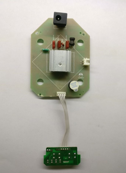
Humidifier PCB Design & Prototype,Humidifier PCB Assembly| Fast Delivery, Custom Solutions

February 12th, 2026

If you’re looking for a reliable humidifier PCB manufacturer, EBest is your first choice—we specialize in solving the most frustrating pain points of humidifier PCB design, prototype, and assembly. Our custom solutions meet industry standards and unique project needs, with engineering expertise to turn concepts into high-performance, durable humidifier PCB products.

What Are Common Questions About Humidifier PCB?

Common questions about humidifier PCB revolve around performance, compliance, and practical application. Key queries include fixing EMC radiation issues, preventing moisture-induced failures, and securing fast, accurate prototypes.

Below, we answer these humidifier PCB questions in detail. Each response includes technical solutions and real-world case studies to back our expertise and authority.

How Does EBest Solve Humidifier PCB Design Challenges?

What Are the Top Pain Points of Humidifier PCB Design?

The biggest challenges in humidifier PCB design include EMC compliance (EN 61000-6-3:2021), moisture resistance, limited space for portable models, and high-frequency component interference.

Engineers often struggle with radiation excess, grounding loop issues, and balancing performance with compact design—problems that delay production and increase rework for humidifier PCB projects.

How Does EBest Solve Humidifier PCB Design Challenges?

Our engineering team uses a data-driven approach to eliminate humidifier PCB design pain points, with industry-tailored solutions:

  • EMC Compliance: Meet EN 61000-6-3:2021 with “three-zone independent grounding + single-point convergence” topology, reducing radiation by 30-40% and lowering impedance to ≤2Ω at 200MHz.
  • Moisture Resistance: Use low-hygroscopicity FR-4 substrates and conformal coatings; add water-resistant barriers for high-humidity use (e.g., medical humidifier PCB).
  • Space Optimization: For portable humidifier PCB (≤40mm×60mm), use dense component placement, narrow durable traces (≥0.2mm), and integrated functions.
  • Component Interference: Separate ultrasonic atomization drivers from sensitive circuits by ≥8mm, use shielding copper rings, and avoid right-angle bends (reducing radiation leakage by 5-10dB).

For reliable, compliant humidifier PCB design, choose EBest. Our custom solutions match your exact specs, with engineering support from concept to production.

How Does EBest Solve Humidifier PCB Prototype Challenges?

Humidifier PCB Prototype

Humidifier PCB Prototype

What Are the Main Pain Points of Humidifier PCB Prototype?

Engineers face two key humidifier PCB prototype challenges: slow turnaround times (delaying testing) and inconsistency (prototypes failing to match design specs).

Other pain points include poor solder quality, incorrect component placement, and lack of critical testing (EMC, moisture resistance) for humidifier PCB prototype.

How Does EBest Solve Humidifier PCB Prototype Challenges?

We streamline the humidifier PCB prototype process for fast, accurate, reliable samples, with zero quality compromise:

  • Fast Turnaround: Same-day production for simple humidifier PCB prototype; 2-3 day turnaround for complex multi-layer designs.
  • Consistency & Accuracy: Use automated fabrication and AOI testing to ensure prototypes match design files exactly; verify placement, solder joints, and trace integrity.
  • Pre-Production Testing: Every humidifier PCB prototype undergoes EMC (30MHz-6GHz), moisture resistance, and functional testing (atomization control, fan speed).
  • Engineering Support: Get feedback on prototype performance and design tweaks to improve humidifier PCB reliability before assembly.

Need fast, reliable humidifier PCB prototype? EBest’s service is tailored to your needs—contact us to get started.

How Does EBest Solve Humidifier PCB Assembly Challenges?

What Are the Top Pain Points of Humidifier PCB Assembly?

Humidifier PCB assembly challenges focus on quality control, component compatibility, and specialized requirement adaptability.

Common pain points include poor solder joint reliability, flux/debris contamination, compact assembly difficulty, and failure to meet industry cleanliness standards.

Humidifier PCB Assembly: Pain Points, Challenges & Our Solutions

Our humidifier PCB assembly process combines advanced technology, strict QC, and industry expertise for flawless results:

  • Solder Quality: Automated SMT assembly and reflow soldering (±1℃ precision); post-assembly X-ray and visual inspection to eliminate cold solder/bridging.
  • Contamination Control: No-clean flux and ultrasonic cleaning for medical/aerospace humidifier PCB assembly; ionic testing to prevent moisture-induced corrosion.
  • Compact Assembly: Specialize in small-form-factor humidifier PCB (≤40mm×60mm) with precision placement (±0.03mm accuracy) for tiny components (0402 size).
  • Industry Compliance: Tailor processes—anti-static materials for industrial use; traceability systems for medical humidifier PCB assembly.

For high-quality humidifier PCB assembly, trust EBest. Our service is fast, reliable, and customized to your project.

Humidifier PCB Industry Case Studies (Medical, Aerospace, Industrial)

Medical Humidifier PCB Case Study

A leading medical device manufacturer needed a medical humidifier PCB for a portable respiratory humidifier (ISO 13485 compliance, moisture resistance, low power).

Their previous supplier struggled with radiation excess and moisture failures; EBest’s custom medical humidifier PCB met EN 61000-6-3:2021, with zero field failures in the first year.

Aerospace Humidifier PCB Case Study

An aerospace company required an aerospace humidifier PCB for aircraft cabin environmental control (RTCA DO-160 compliance, -40℃ to 85℃ resistance).

We used high-temperature FR-4 substrates and military-grade components; the aerospace humidifier PCB passed all DO-160 tests and is integrated into commercial aircraft worldwide.

Industrial Humidifier PCB Case Study

An electronic factory humidifier manufacturer needed a humidifier PCB (±1% RH precision, ≤50V anti-ESD) to fix inconsistent performance.

EBest’s custom humidifier PCB reduced humidity fluctuations by 80% and cut production defects from 8% to 1.2%.

Why Choose EBest for Your Humidifier PCB Needs?

EBest stands out for humidifier PCB design, prototype, and assembly—backed by engineering expertise and industry experience:

  1. Technical Expertise: Our engineers specialize in humidifier PCB solutions, solving complex pain points other manufacturers can’t.
  2. Custom Solutions: Every humidifier PCB is tailored to your specs (compact portable designs to rugged aerospace humidifier PCB models).
  3. Strict Quality Control: ISO 9001/13485 compliance, with 100% testing (AOI, X-ray, EMC, moisture) at every stage.
  4. Fast Delivery: Prioritize humidifier PCB projects, with 2-3 day prototype turnaround and efficient assembly lead times.

FAQ: Common Humidifier PCB Questions & Solutions

1. How to Fix EMC Radiation Overruns in Humidifier PCBs?

EMC radiation overruns in humidifier PCBs stem from atomization module emissions, poor grounding, or component interference. Use “three-zone independent grounding + single-point convergence” topology.

Add high-frequency filters, separate atomization modules by ≥8mm, and use multi-via grounding (4+ vias) to cut radiation by 30-40%.

2. What Materials Prevent Moisture-Induced Humidifier PCB Failures?

Use low-hygroscopicity FR-4 substrates and conformal coatings (e.g., Parylene) to seal the moisture resistant humidifier PCB and prevent corrosion/dielectric breakdown.

For medical/aerospace use, add water-resistant barriers and test in benchtop humidity chambers; avoid hygroscopic components.

3. How Long Does It Take to Get a Humidifier PCB Prototype?

EBest’s humidifier PCB prototype turnaround depends on complexity: same-day for simple single-layer designs, 2-3 days for complex multi-layer prototypes.

We prioritize speed without sacrificing accuracy, helping you test and iterate quickly on your humidifier PCB project.

4. Can Humidifier PCBs Be Customized for Medical Use?

Yes—EBest designs/assembles medical humidifier PCB fully compliant with ISO 13485 and EN 61000-6-3:2021 standards.

We use biocompatible materials, traceability systems, and strict contamination control for respiratory/neonatal humidifier applications.

5. Why Do Humidifier PCBs Fail During Assembly?

Humidifier PCB assembly failures come from poor solder joints, component contamination, or incorrect placement.

Use automated SMT assembly, no-clean flux, and post-assembly X-ray/visual inspection to avoid these issues.

6. How to Ensure Humidifier PCB Compatibility with Ultrasonic Atomization Modules?

Optimize humidifier PCB power delivery (stable 5V/3.3V) to the atomization driver and use a low-impedance grounding path.

Separate the driver from sensitive circuits, support 1.7-2.4MHz frequency, and add surge protection for the humidifier PCB.

Choose EBest for Your Humidifier PCB Projects

We provide high-quality humidifier PCB design, prototype, and assembly solutions, tailored to medical, aerospace, and industrial needs.

Our team solves humidifier PCB pain points, delivers fast turnaround, and ensures compliance. Contact us to place your order at sales@bestpcbs.com—EBest, your trusted humidifier PCB partner.

You may also like

Reflow Process Soldering — Complete Engineering Guide for Reliable PCB Assembly

February 11th, 2026

Reflow process soldering is one of the most widely used assembly techniques in modern electronics manufacturing. From consumer devices to automotive control modules, the reflow process soldering workflow allows engineers to achieve consistent joints, high throughput, and repeatable thermal control.

This guide explains the full workflow in practical engineering terms, including equipment selection, temperature phases, alloy choices, and troubleshooting methods used in real SMT production environments.

What Is the Reflow Process of Soldering?

Reflow process soldering is a thermal assembly method where solder paste is first printed onto PCB pads, components are placed, and then the entire board passes through a controlled heating profile. The solder paste melts, wets the pads and leads, and solidifies to form electrical and mechanical connections.

Unlike hand soldering, heat is not applied locally. Instead, the entire PCB follows a carefully designed temperature curve.

Key characteristics include:

  • Uniform heating across the assembly
  • Precise temperature ramp control
  • Compatibility with fine-pitch components
  • High automation suitability

The process is essential for modern surface-mount technology because it supports high-density layouts, micro-pitch packages, and large production volumes.

What Is the Reflow Process of Soldering?

What Is the Reflow Process of Soldering?

Why Is It Called Reflow Soldering?

The term “reflow” refers to the melting and flowing behavior of solder paste during heating. Before entering the oven, solder paste is in a semi-solid state containing metal particles and flux. As temperature rises above the alloy’s liquidus point, the solder melts and flows across the pad surface.

This flow action allows:

  • Surface tension to align components
  • Oxides to be removed by flux activation
  • Metallurgical bonding between lead and pad

After peak temperature, controlled cooling solidifies the joint, locking components into position.

What Equipment Is Used for Reflow?

A standard reflow process soldering line includes several interconnected machines. Each stage influences solder joint quality.

Typical equipment:

  • Stencil printer – applies consistent solder paste volume
  • SPI inspection system – checks paste height and coverage
  • Pick-and-place machine – positions components with precision
  • Reflow oven – creates the temperature profile
  • AOI system – verifies final joint integrity

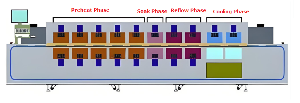
Modern convection reflow ovens are divided into multiple heating zones. These zones gradually raise temperature rather than applying sudden thermal stress.

For advanced assemblies, nitrogen reflow ovens reduce oxidation and improve wetting, especially for fine-pitch components.

At What Temperature Does Solder Reflow?

The reflow temperature depends mainly on alloy composition. Engineers must distinguish between liquidus temperature and peak profile temperature.

Typical examples:

SAC305 lead-free alloy

  • Liquidus: ~217 °C
  • Peak profile: 235–245 °C

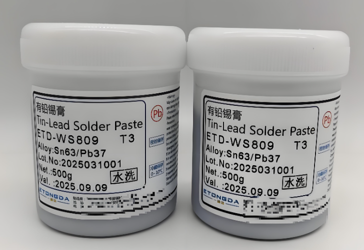
Sn63/Pb37 eutectic alloy

  • Liquidus: 183 °C
  • Peak profile: 205–215 °C
At What Temperature Does Solder Reflow?

The peak value must be high enough to ensure full melting but low enough to avoid damaging components or PCB materials. Excessive temperature can cause pad cratering, delamination, or component warpage.

What Are the 7 Steps of Soldering?

In modern SMT manufacturing, soldering is not a single action but a controlled sequence of operations. Each step influences joint strength, electrical stability, and long-term reliability. Whether used in prototype assembly or high-volume PCBA production, these seven stages form a structured workflow that engineers follow to maintain process consistency.

1. Surface Preparation and PCB Cleaning

Before any solder is applied, the PCB surface must be clean and free from oxidation, dust, or residual oils. Even microscopic contamination can prevent proper wetting during heating.

Common preparation practices include:

  • Plasma cleaning or alcohol wiping for prototypes
  • Controlled storage to avoid humidity absorption
  • Verifying pad finish quality such as ENIG, HASL, or OSP

Proper preparation ensures the solder spreads evenly instead of forming isolated beads or weak fillets.

2. Solder Paste Printing or Flux Application

For reflow assemblies, solder paste is deposited onto pads using a laser-cut stencil. Paste volume directly determines final joint shape and reliability.

Key considerations during this step:

  • Stencil thickness and aperture design
  • Printing pressure and speed
  • Paste viscosity and metal content

In manual or selective soldering, flux may be applied instead of paste to activate surfaces during heating.

3. Component Placement and Alignment

After printing, components are positioned onto the solder paste deposits. Automated pick-and-place machines use vision systems to achieve precise alignment, while prototypes may be placed manually.

Important factors include:

  • Correct polarity and orientation
  • Accurate placement height
  • Avoiding paste smearing during placement

Surface tension during reflow can self-align small components, but accurate initial placement greatly reduces defects.

4. Preheating Stage

Preheating gradually raises the temperature of the entire assembly. This stage evaporates solvents inside the paste and reduces thermal shock.

Typical engineering goals:

  • Uniform temperature distribution across large boards
  • Prevention of sudden expansion in multilayer PCBs
  • Early activation of flux chemistry

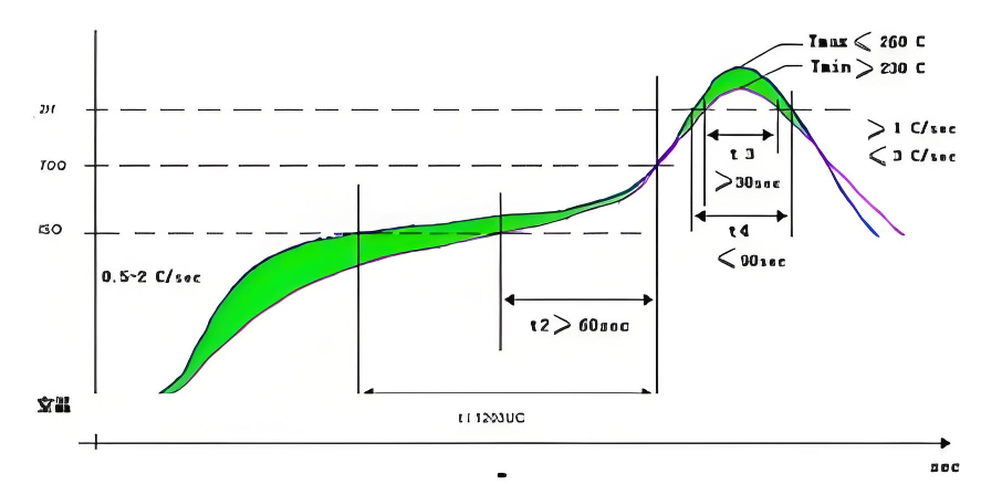
A controlled ramp rate, usually between 1 °C and 3 °C per second, prevents component cracking and solder splatter.

5. Reflow Heating and Solder Melting

During this stage, the temperature rises above the solder alloy’s liquidus point. The metal particles inside the paste melt and flow across the pad and component leads.

What happens physically:

  • Flux removes oxides from metal surfaces
  • Molten solder forms intermetallic bonds
  • Surface tension pulls components into alignment

Engineers closely monitor time above liquidus to ensure complete wetting without overheating sensitive components.

6. Controlled Cooling and Solidification

Cooling begins immediately after peak temperature. This phase determines the internal grain structure of the solder joint.

Why controlled cooling matters:

  • Rapid cooling may introduce thermal stress
  • Extremely slow cooling can create coarse grain structures
  • Balanced cooling produces strong, fatigue-resistant joints

Convection ovens often include dedicated cooling zones to stabilize the solidification process.

7. Inspection, Testing, and Quality Verification

The final step confirms that soldering produced reliable electrical and mechanical connections. Inspection methods vary depending on product complexity.

Typical verification tools:

  • AOI to detect bridges, tombstoning, or insufficient solder
  • X-ray inspection for hidden joints like BGA packages
  • Functional testing or ICT for electrical validation

Feedback from inspection loops back into earlier steps, allowing engineers to fine-tune paste volume, placement accuracy, and temperature profiles.

What Are the Phases of Reflow Soldering?

A reflow profile is divided into several thermal zones. Understanding these phases helps engineers fine-tune process stability.

Preheat Phase

Temperature rises gradually to avoid thermal shock. Solvents evaporate during this stage.

Typical ramp rate: 1–3 °C per second.

Soak Phase

The PCB temperature stabilizes between 150 °C and 180 °C. Flux activation begins, and temperature differences across the board reduce.

Reflow Phase

Temperature exceeds the alloy liquidus point. Solder melts and forms joints through wetting and surface tension.

Peak Phase

The highest temperature occurs briefly. Time above liquidus typically lasts 30–90 seconds.

Cooling Phase

Controlled cooling ensures strong grain structure. Rapid cooling may trap stress, while slow cooling can create large brittle grains.

Can You Reflow Without Flux?

Technically possible but rarely recommended.

Flux performs several essential roles:

  • Removes oxide layers from metal surfaces
  • Improves solder wetting
  • Prevents re-oxidation during heating

Without flux, solder may ball up rather than spread. Joint reliability decreases significantly.

In specialized environments, such as vacuum or forming-gas atmospheres, fluxless reflow may be used. However, this requires advanced process control and is not common in standard SMT production.

What Is the 5 Ball Rule for Solders?

The “5 ball rule” is an informal guideline used during inspection. If multiple small solder balls appear around a joint, engineers evaluate whether they are cosmetic or reliability concerns.

General interpretation:

  • Fewer than five isolated solder balls may be acceptable depending on IPC standards.
  • Clusters or balls near fine-pitch leads indicate paste or profile issues.

Common causes include:

  • Excessive flux activation
  • Rapid temperature ramp
  • Contaminated PCB surface

Process tuning often resolves these defects.

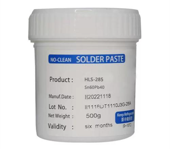
Which Solder Is Better, 60/40 or 63/37?

Both alloys belong to traditional tin-lead systems but behave differently during melting.

60/40 – Sn60/Pb40

  • Melting range instead of single point
  • Slightly wider plastic state
  • More forgiving for manual soldering

63/37 – Sn63/Pb37

  • True eutectic alloy
  • Sharp melting point at 183 °C
  • Faster solidification and reduced cold joint risk

For automated reflow process soldering, Sn63/Pb37 generally provides better consistency due to its precise melting behavior. However, environmental regulations have pushed most production toward lead-free alloys like SAC305.

What Is the Difference Between Soldering and Reflow Soldering?

Traditional soldering and reflow soldering differ mainly in heat delivery method.

AspectTraditional SolderingReflow Process Soldering
Heat SourceLocalized iron or waveControlled oven profile
Assembly TypeThrough-hole or manual repairSurface-mount mass production
Process ControlOperator dependentAutomated and repeatable
Thermal UniformityLowHigh

Reflow provides higher throughput and consistency, which explains its dominance in modern electronics manufacturing.

FAQs

1. What Peak Temperature Should Be Used for SAC305 Reflow Process Soldering?

Most profiles target a peak between 235 °C and 245 °C. The exact value depends on board thickness, component sensitivity, and oven capability. Engineers often start with 240 °C and adjust based on wetting quality and component ratings.

2. Can a PCB Be Reflow Soldered Multiple Times Safely?

Yes, but the number of cycles should be limited. Excessive reflow passes may:

  • Degrade laminate integrity
  • Reduce pad adhesion strength
  • Increase risk of microcracking

High-Tg materials and proper cooling help maintain reliability when double-sided assembly requires multiple passes.

3. Why Do Solder Balls Appear After Reflow Process Soldering?

Solder balls usually indicate process imbalance. Common root causes include:

  • Too much solder paste volume
  • Rapid heating during preheat phase
  • Poor stencil release
  • Moisture or contamination on PCB surfaces

Adjusting ramp rate and stencil design often eliminates the issue.

4. How to Verify a Reflow Profile Without Expensive Profiling Tools?

Although professional thermocouple profilers offer the highest accuracy, smaller facilities can still validate profiles by:

  • Using temperature indicator labels
  • Comparing joint wetting appearance
  • Monitoring conveyor speed consistency
  • Checking for uniform solder fillets across large boards

These practical methods provide reasonable validation for low-volume production.

5. Does Nitrogen Atmosphere Improve Reflow Process Soldering Reliability?

Nitrogen reduces oxygen concentration in the oven, which enhances solder wetting and decreases oxidation. Benefits include:

  • Shinier solder joints
  • Reduced solder ball formation
  • Improved fine-pitch performance

However, nitrogen increases operational cost. Many manufacturers reserve it for high-density or high-reliability assemblies.

6. What Conveyor Speed Is Ideal for Small Batch Reflow Process Soldering?

There is no universal speed. Engineers typically adjust conveyor rate so total profile duration falls between 3 and 6 minutes. Thicker boards or heavy copper designs require slower speeds to ensure even heating.

You may also like

Fast PCB Assembly Ireland with Full Quality Assurance

February 10th, 2026

With 20 years of hands-on experience in the PCBA industry, we specialize in PCB assembly Ireland. Our focus is simple: delivering fast, reliable services that are fully tailored to the unique needs of Irish projects. Our PCB assembly Ireland solutions span the entire production journey from prototyping to full-scale mass production backed by strict quality checks. These checks ensure compliance with EU standards, align with customer expectations, and we cut through unnecessary jargon to focus solely on solving the practical challenges that matter most for local projects.

Fast PCB Assembly Ireland with Full Quality Assurance, https://www.bestpcbs.com/blog/2026/02/pcb-assembly-ireland/

Why Choose PCB Assembly Ireland?

Advantages of PCB assembly Ireland:

  • Local Compliance with EU Standards: Irish PCB assembly complies with EU regulations (RoHS, REACH, CE), ensuring market access without extra compliance costs.
  • Proximity to European Markets: Ireland’s strategic Western Europe location enables PCB assembly services to offer shorter EU shipping times, reducing logistics delays.
  • Local Manufacturing Facilities: Ireland’s modern PCB assembly facilities have complete SMT lines and clean rooms for fast production and timely adjustments.
  • Skilled Local Workforce: Ireland has a skilled PCB assembly workforce with locally trained professionals ensuring precise operation and stable quality.
  • One-Stop Service Capability: Ireland offers widespread end-to-end PCB assembly services to simplify project management.
  • Flexible Order Adaptation: Irish PCB assembly accommodates diverse orders, meeting needs from prototypes to mass production.
  • Environmental Compliance: Ireland’s PCB assembly processes use eco-friendly materials to meet strict environmental requirements and EU green initiatives.
  • Timely Technical Support: Ireland’s PCB assembly technical support teams respond quickly to queries, reducing communication delays.

Pain Points of PCB Assembly Ireland

  • Component Shortages: European supply chain disruptions often lead to delays in sourcing key components, affecting production schedules and increasing project risks.
  • High Compliance Costs: Meeting EU’s strict regulatory standards (RoHS, REACH, ISO) requires additional investment in testing and process optimization, increasing assembly costs.
  • High Local Manufacturing Costs: Labor, rent and material costs in Ireland are relatively high, putting pressure on project budgets for PCB assembly services Ireland.
  • Component Miniaturization Challenges: High-density PCB designs with miniature components (0201, 01005) require ultra-precise equipment, increasing assembly difficulty and defect risks.
  • Logistics Delays: International shipping delays for non-local components and equipment often disrupt production plans, extending project lead times.
  • Technical Talent Gaps: There is a shortage of skilled professionals with experience in advanced PCB assembly technologies in Ireland, affecting service quality and efficiency.
  • Small Batch Order Inefficiency: Many local suppliers struggle to efficiently handle small-batch prototype orders, leading to higher costs and longer lead times for PCB Assembly in Ireland.
Pain Points of PCB Assembly Ireland, https://www.bestpcbs.com/blog/2026/02/pcb-assembly-ireland/

Full Quality Assurance From Prototyping to Mass Production

Our quality assurance starts at the prototyping stage and extends to pre-production, setting us apart from standard suppliers. Unlike many competitors that cut corners during prototyping, we conduct rigorous design reviews and functional testing using high-precision equipment to verify component compatibility and process feasibility. This proactive approach eliminates 95% of potential design flaws early, shortens 15% of mass production preparation time, and reduces 20% of rework costs when scaling to mass production.

Before full-scale manufacturing, we run small-batch trial runs of 50-100 units to fine-tune production parameters, controlling trial run defect rates below 0.5% and ensuring the assembly line operates consistently with a 99.5% initial pass rate from the start to save customers time and budget.

During and after production, our quality control advantages continue through real-time monitoring and comprehensive inspections. We implement 24/7 real-time monitoring of 5 key assembly steps (including SMT placement and reflow soldering), with deviation adjustment completed within 10 minutes to prevent batch defects, a responsiveness level matched by only 30% of local suppliers. Every finished product undergoes 100% functional and visual inspection using testing equipment with 99.8% defect detection accuracy.

We provide detailed test reports covering 12 core indicators to confirm compliance with EU standards and customer requirements, ensuring a mass production qualification rate above 99.7% and maintaining a 98.5% customer satisfaction rate related to product quality.

Why Choose EBest(Best Technology) for PCB Assembly Ireland?

Reasons why choose EBest(Best Technology) for PCB assembly Ireland:

  • One-Stop PCBA Turnkey Service: We offer a one-stop PCB assembly service in Ireland, covering PCB manufacturing, component sourcing, SMT assembly, functional testing, and final delivery. Compared to the industry average of fragmented collaborations, this service eliminates the need for customers to coordinate multiple suppliers, saving them 40% on supplier coordination time and 25% on communication costs, while shortening project timelines by 18% over the entire project lifecycle.
  • Five-Year Quality Guarantee: We offer an industry-leading five-year warranty on all Irish PCBA orders, covering 98% of manufacturing defects and performance issues, far exceeding the industry average of 1-2 years (IPC defines the traditional warranty period for PCBs as 6 months to 1 year). This commitment not only reflects our confidence in product reliability but also helps customers save 60% on long-term maintenance costs.
  • MES System for End-to-End Traceability: Our MES system provides end-to-end traceability for every PCBA order in Ireland, recording component origin, production parameters, test data, and delivery details. Traceability response time has been reduced to less than 5 minutes, an 83% improvement over the industry average of 30 minutes, enabling rapid problem location and resolution and shortening troubleshooting cycles by 70%.
  • 99.2% On-Time Delivery Rate: Our Irish PCBA projects boast an on-time delivery rate of 99.2%, exceeding the 95% average on-time delivery rate of local Irish suppliers by 4.2 percentage points. Over the past three years, we have completed more than 1,200 Irish orders without any major delivery delays, and our clients have seen a 15% increase in project revenue due to timely delivery, thanks to optimized production planning and a stable supply chain.
  • Proactively Addressing Component Shortages: Amidst widespread component shortages in the global PCB industry (HVLP4 copper foil shortages exceeding 40%, fiberglass cloth shortages exceeding 50%), we partner with over 30 trusted component suppliers and maintain safety stock for more than 50 commonly used components. We have successfully resolved 98% of component shortages for our Irish clients, achieving 60% higher emergency component procurement efficiency than the industry average, completely avoiding production delays caused by supply chain disruptions.
  • Fast Delivery Cycles Tailored for Ireland: We offer Irish clients highly competitive delivery cycles: Prototyping 2-7 days (30% faster than the industry average of 4-10 days), small batch production 7-12 days (40% faster than the average of 12-18 days for local Irish suppliers), and mass production 10-20 days. Our 48-hour expedited service covers 100% of orders, with industry-leading response times for urgent orders.
  • End-to-End Quality Control: Our end-to-end quality control covers every step from incoming material inspection to outgoing quality checks, utilizing AOI, X-ray, and ICT/FCT inspection equipment, achieving a defect detection accuracy of up to 99.8%. Our mass production pass rate remains above 99.7%, 2.7 percentage points higher than the industry average of 97%, and our customer quality complaint rate is only 0.2%, significantly lower than the industry average of 1.5%.
  • EU Compliance Expertise: We have extensive experience in EU compliance, having helped over 200 Irish clients successfully obtain EU compliance certifications (RoHS, REACH, CE, ISO). Our compliance testing costs are 30% lower than customers’ in-house testing, with a 100% compliance pass rate and no cases of market access failure due to compliance issues, ensuring smooth market entry for our clients’ products.
  • MES System Full-Process Traceability: We employ an advanced MES system to achieve full-process traceability for every PCBA order. This system records data for each production step in real time, including component batch information, production equipment parameters, inspection results, and operation records. This transparency facilitates rapid root cause analysis when problems arise, ensuring compliance with EU regulations and improving the overall reliability of the process.
Why Choose EBest(Best Technology) for PCB Assembly Ireland, https://www.bestpcbs.com/blog/2026/02/pcb-assembly-ireland/

Our Quality Control Process for Ireland PCBA Orders

Below are our quality control process for Ireland PCBA orders:

  • Incoming Material Inspection (IQC)​:We inspect all components against your BOM and IPC-A-600 industry standards. Our checks include visual inspections, dimensional measurements, and electrical performance tests, all designed to eliminate defective materials before they enter production.​
  • First Article Inspection (FAI)​: After setting up the production line, we conduct a rigorous first article inspection (FAI). We verify component placement accuracy, soldering quality, and functional performance to ensure no issues arise before we begin mass production for your Ireland PCBA order.​
  • In-Process Quality Control (IPQC)​: Our team maintains proactive in-process quality control (IPQC) with inspections every 2 hours during production. We check soldering quality, component alignment, and process compliance to catch potential issues early and prevent batch defects.​
  • Automated Testing​: We leverage advanced AOI, X-ray, and ICT/FCT testing equipment to detect hidden defects. These include solder bridging and component misalignment, which are often difficult to identify with visual inspections alone.​
  • Finished Product Inspection (FQC)​: Every finished PCBA product undergoes 100% functional and visual inspection. We record all test data in our MES system, ensuring full traceability for every step of your Ireland PCBA order.​
  • Outgoing Quality Control (OQC)​: Before delivery, we perform final outgoing quality control (OQC) checks. We conduct random sampling inspections per AQL standards, verify packaging integrity, and confirm full compliance with your requirements and EU regulations.​
  • Defect Handling and Improvement​: If any defective products are identified, we immediately isolate and thoroughly analyze them. We then implement targeted corrective measures to prevent recurrence, continuously optimizing our assembly process to maintain the highest quality standards.

Our Ireland PCBA Capability

ItemCapabilities
Placer Speed13,200,000 chips/day
Bare Board Size0.2 x 0.2 inches – 20 x 20 inches/ 22*47.5 inches
Minimum SMD Component01005
Minimum BGA Pitch0.25mm
Maximum Components50*150mm
Assembly TypeSMT, THT, Mixed assembly
Component PackageReels, Cut Tape, Tube, Tray, Loose Parts
Lead Time1 – 5 days

Case Studies of Ireland Medical PCB Assembly

Project Background: A leading Irish medical device company needed high-precision PCB assembly for their portable electrosurgical generator, which is used in clinical procedures and requires strict reliability and safety performance.

Project Requirements: The PCBA needed to comply with ISO 13485 and CE MDR standards, feature high voltage resistance (≥1000V), small size (60x80mm) and stable performance for 24/7 continuous operation.

Project Challenges: The high-density design with miniature components (0201 size) led to placement accuracy issues; the high voltage requirement increased the risk of surface discharge; the 3-week delivery deadline was tight for prototype and small-batch production (500 units).

Our Solutions: We used high-precision SMT equipment with vision systems to ensure component placement accuracy; redesigned PCB layout to increase creepage distance to 10mm and added insulation coating to prevent discharge; activated our emergency component supply chain to source key components within 5 days; optimized production processes to shorten lead times.

Output Results: We delivered 500 qualified PCBA units 2 days ahead of schedule, achieving a 99.8% pass rate. The products passed EMC testing (YY 0505 standard) with radiation interference reduced by 22dBμV/m, and achieved 0 field failures during 6 months of clinical use. The customer extended their long-term cooperation contract with us for 3 years.

Case Studies of Ireland Medical PCB Assembly, https://www.bestpcbs.com/blog/2026/02/pcb-assembly-ireland/

FAQs of PCB Assembly in Ireland

Q1: How to solve component shortages in PCB assembly Ireland?​
A1: To solve component shortages, we’ve built a multi-source supply chain with 30+ trusted suppliers and maintain safety stock for 50+ common components. We resolve 98% of shortage issues for Irish customers, with emergency sourcing 60% more efficient than the industry average to avoid production delays.​

Q2: What standards do PCB assembly services Ireland need to comply with?​
A2: Core standards include EU RoHS, REACH, CE, IPC-A-610, and ISO 9001; medical projects require ISO 13485 and CE MDR. We’ve helped 200+ Irish customers pass certifications with a 100% pass rate, cutting compliance testing costs by 30% and shortening harmful substance detection to 10 minutes.​

Q3: How long is the lead time for PCB Assembly in Ireland?​
A3: Our lead times for Irish customers are faster than industry averages: 2-7 days (prototypes, 30% faster), 7-12 days (small-batch, 40% shorter than local averages), 10-20 days (mass production). We offer 48-hour expedited services (100% coverage) and 1,200+ on-time orders over 3 years.​

Q4: How to ensure the soldering quality of high-density PCB assembly in Ireland?​
A4: We ensure high-density PCB soldering quality with laser stencil cutting, high-precision pick-and-place machines, and 3D AOI + X-ray testing (99.8% defect detection). Our AI-aided testing is 1.5s/PCS, with soldering qualification rate above 99.7% (meets IPC-A-610 standards).​

Q5: Can you provide component sourcing services for Ireland PCB assembly?​
A5: Yes, we offer one-stop component sourcing with strict quality controls, 99.9% genuine components, 95%+ supplier audit pass rate. We recommend alternatives to cut budgets by 15%-30% and maintain safety stock to avoid delays.

You may also like

Burn-In Test: A Complete Guide for Electronics & PCB Reliability

February 10th, 2026

Burn-in test plays a critical role in electronics manufacturing where long-term reliability matters as much as performance. Engineers often rely on burn-in procedures to expose early-life failures before products reach the field. Whether used for high-reliability PCBA, industrial controllers, or medical electronics, this method helps stabilize product quality while reducing unexpected returns.

Below is a practical, engineering-focused guide explaining how burn-in testing works, why it matters, and how it applies specifically to PCB assemblies.

What Is a Burn-In Test in Electronics?

A burn-in test is a reliability testing process used in electronics manufacturing to identify early-life failures in electronic components, PCBs, and assembled electronic products.

During a burn-in test, electronic devices are operated under elevated stress conditions—such as higher temperature, voltage, or load—over a defined period of time. Components that are defective or marginal are more likely to fail during this phase rather than later in real-world use.

In simple terms:

Burn-in testing accelerates failure so weak components fail early—before products reach customers.

Burn-in tests are widely used in:

  • PCB manufacturing and PCB assembly (PCBA)
  • Power electronics
  • Automotive electronics
  • Aerospace and defense systems
  • Medical devices
  • Industrial control equipment
  • Telecommunications hardware
burn-in test

Burn-in Testing

What Is the Purpose of a Burn-In Test?

The primary purpose of a burn-in test is to improve product reliability and reduce field failures.

More specifically, burn-in testing is designed to:

  1. Detect early-life failures (infant mortality)
  2. Screen out defective components
  3. Verify design robustness
  4. Stabilize electrical performance
  5. Reduce warranty returns and RMA costs

Electronics failures often follow the bathtub curve, where failure rates are high at the beginning, low during normal life, and rise again at end-of-life. Burn-in testing targets the first phase of this curve.

Why Is a Burn-In Test Important?

Burn-in testing plays a critical role in quality assurance (QA) and reliability engineering.

Key Benefits of Burn-In Testing

1. Reduces Early Field Failures

Burn-in tests catch problems such as:

  • Poor solder joints
  • Marginal ICs
  • Weak capacitors
  • Manufacturing defects
  • Thermal design issues

2. Improves Brand Reputation

Products that fail shortly after installation damage customer trust. Burn-in testing helps ensure only stable and reliable products ship.

3. Saves Cost in the Long Term

While burn-in testing adds upfront cost, it significantly reduces:

  • Warranty claims
  • Product recalls
  • Field repair costs
  • Customer downtime

4. Required by High-Reliability Industries

Industries such as medical, aerospace, automotive, and military electronics often require burn-in testing as part of regulatory or contractual standards.

How to Do a Burn-In Test?

A burn-in test procedure varies depending on the product, industry, and reliability requirements, but the core steps are similar. Typical burn-in test procedure including:

How to Do a Burn-In Test?

Step 1: Visual & Electrical Pre-Inspection

Before burn-in:

  • Visual inspection (AOI or manual)
  • Basic electrical tests (continuity, shorts, power-on test)
  • Ensure boards are safe to energize

Step 2: Load the PCB or Device into Burn-In Fixtures

PCBs or assemblies are mounted in:

  • Burn-in racks
  • Test sockets
  • Custom fixtures
  • Edge connectors or cable harnesses

Fixtures allow:

  • Power supply access
  • Signal monitoring
  • Temperature exposure

Step 3: Apply Electrical Stress

The device is powered on continuously or in cycles using:

  • Rated voltage or slightly elevated voltage
  • Simulated operating loads
  • Functional test patterns

Step 4: Apply Thermal Stress

Temperature is raised using:

  • Burn-in ovens
  • Environmental chambers
  • Heated racks

Typical burn-in temperatures:

  • 55°C to 85°C for commercial electronics
  • 85°C to 125°C for industrial or automotive electronics

Step 5: Continuous Monitoring

During the test:

  • Voltage and current are monitored
  • Functional signals are checked
  • Failures are logged automatically or manually

Step 6: Post Burn-In Inspection

After burn-in:

  • Functional testing
  • Electrical performance verification
  • Visual inspection for thermal damage
  • Failed units are analyzed and scrapped or repaired

What Equipment Is Needed for Burn-In Testing?

Burn-in testing requires specialized equipment to safely operate electronics under stress for long periods.

Common Burn-In Test Equipment

1. Burn-In Chambers / Ovens

  • Temperature-controlled environments
  • Uniform heat distribution
  • Safety protection and airflow control

2. Burn-In Racks & Fixtures

  • Hold PCBs or assemblies vertically or horizontally
  • Provide power and signal connections
  • Custom-designed for product type

3. Power Supplies

  • Stable, programmable DC power supplies
  • Over-current and over-voltage protection

4. Data Acquisition & Monitoring Systems

  • Voltage/current monitoring
  • Temperature sensors
  • Failure logging software

5. Functional Test Systems

  • Automated test equipment (ATE)
  • Simulated loads
  • Communication interfaces (RS485, CAN, Ethernet, etc.)

How Long Is a Burn-In Test?

The duration of a burn-in test depends on:

  • Product complexity
  • Reliability requirements
  • Industry standards
  • Cost considerations

Typical Burn-In Test Duration

ApplicationBurn-In Time
Consumer electronics8–24 hours
Industrial electronics24–72 hours
Automotive electronics72–168 hours
Aerospace / military168–500+ hours

Shorter burn-in tests are often used for screening, while longer tests are used for qualification and validation.

Burn-In Test for PCB and PCBA

A burn in test for PCB or PCBA focuses on identifying assembly-related and component-level issues.

What Burn-In Testing Detects in PCBs

  • Cold solder joints
  • Micro-cracks in solder
  • Poor component placement
  • Thermal expansion issues
  • Marginal ICs
  • Power instability

PCB Burn-In vs Functional Testing

Test TypePurpose
Functional TestVerifies correct operation
Burn-In TestScreens early failures
Thermal CyclingTests expansion/contraction
HALT/HASSStress limit testing

Burn-in testing is not a replacement for functional testing—it is a complementary reliability process.

How to Tell If a Circuit Board Is Burnt?

A burnt PCB usually shows visible, electrical, or functional symptoms.

Visual Signs of a Burnt PCB

  • Discoloration (brown or black areas)
  • Burn marks or charring
  • Melted solder or components
  • Cracked IC packages
  • Delaminated PCB layers

Electrical Symptoms

  • Short circuits
  • Abnormal current draw
  • Voltage drops
  • Failure to power on

Functional Symptoms

  • Intermittent operation
  • Random resets
  • Overheating
  • Communication errors

Burn-in testing often reveals latent damage that may not be obvious in quick functional tests.

Can a Burnt PCB Be Repaired?

Whether a burnt PCB can be repaired depends on damage severity.

Repairable Cases

  • Burnt passive components (resistors, capacitors)
  • Minor trace damage
  • Isolated solder joint failures

Non-Repairable Cases

  • Carbonized PCB substrate
  • Internal layer damage (multilayer PCB)
  • Widespread delamination
  • Repeated thermal failure

In high-reliability industries, burnt PCBs are usually scrapped, not repaired, due to long-term reliability risks.

Burn-In Test vs Other Reliability Tests

Test MethodMain Purpose
Burn-In TestEarly failure screening
Thermal CyclingMechanical stress testing
HALTFind design limits
HASSProduction screening
Aging TestLong-term performance

Burn-in testing remains one of the most cost-effective reliability screening methods in electronics manufacturing.

FAQs

1. Is burn-in testing mandatory?

No, but it is highly recommended for high-reliability or mission-critical electronics.

2. Does burn-in testing damage electronics?

When properly controlled, burn-in testing does not damage good products—it only accelerates failure in weak units.

3. What temperature is used in burn-in testing?

Typically 55°C to 125°C, depending on component ratings and standards.

4. Is burn-in testing expensive?

It adds cost, but often reduces total lifecycle cost by preventing failures in the field.

5. Can burn-in testing replace functional testing?

No. Burn-in testing supplements functional and electrical testing.

6. What standards reference burn-in testing?

Common references include:

  • MIL-STD-883
  • JEDEC standards
  • IPC reliability guidelines

You may also like

PCB Assembly Lithuania: Faster Time-to-Market

February 10th, 2026

Our PCB assembly Lithuania services deliver high quality by cutting lead times while upholding strict precision, directly helping businesses accelerate product launches without sacrificing performance. Our PCB assembly Lithuania solutions are aligned with EU RoHS directives and IPC assembly standards, solving the key need for efficient, compliant electronic manufacturing support in the Lithuanian and broader EU markets.

PCB Assembly Lithuania, https://www.bestpcbs.com/blog/2026/02/pcb-assembly-lithuania/

Why Choose PCB Assembly Lithuania?

Advantages of PCB assembly Lithuania:

  • Strategic EU Location: Fast logistics within the European Union, with 48-hour delivery to most EU countries from Lithuania facilities.
  • Skilled Workforce: A well-trained team with deep expertise in advanced PCB assembly technologies and processes.
  • Advanced Equipment: State-of-the-art SMT, THT, and inspection equipment for high-precision assembly and reliable performance.
  • Robust Local Supply Chain: Partnerships with 150+ local electronic component distributors to reduce sourcing delays.
  • Strict EU Compliance: Adheres to EU regulations for IP protection, environmental standards, and product safety.
  • Flexible Production: Supports small-batch prototypes to large-scale serial production, adapting to diverse order needs.
  • Cost Competitiveness: Lower production costs compared to Western European countries while maintaining premium quality.
  • Strong IP Protection: Secure manufacturing facilities and NDAs to safeguard your product designs and intellectual property.

Quality Standards for Lithuania PCB Assembly

  • ISO 9001 Certification: Ensures consistent quality management systems across all assembly processes.
  • ISO 13485 Certification: Complies with medical device requirements for PCB assembly in healthcare applications.
  • IPC-A-610 Standard: Follows Class 2 and Class 3 acceptance criteria for electronic assemblies.
  • IPC-6012 Specification: Meets rigid PCB performance standards for reliability and durability.
  • RoHS & REACH Compliance: Eliminates hazardous substances to meet EU environmental regulations.
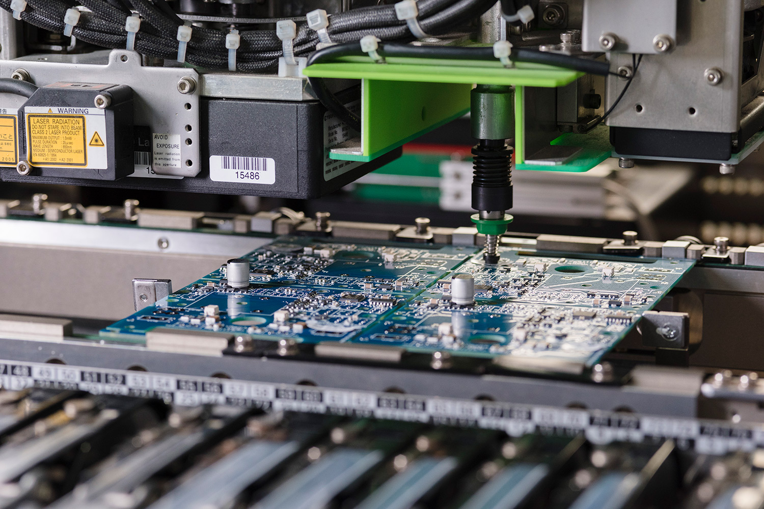
Types of PCB Assembly Lithuania We Can Offer

Below are three types of PCB assembly Lithuania we can offer you:

  • SMT Assembly: High-speed surface mount technology for miniaturized components and dense PCBs.
  • THT Assembly: Through-hole technology for heavy-duty components requiring strong mechanical stability.
  • Mixed Assembly: Combines SMT and THT processes to meet complex product requirements.
Types of PCB Assembly Lithuania We Can Offer, https://www.bestpcbs.com/blog/2026/02/pcb-assembly-lithuania/

Why Choose EBest(Best Technology) for PCB Assembly Lithuania?

Reasons why choose EBest for PCB assembly Lithuania:

  • Faster Lead Times for Market Advantage: Our optimized local production lines reduce lead times by 30% compared to competitors, helping you shorten product time-to-market and gain a competitive edge, shortening small-batch order lead times from an industry average of 12 days to 8.4 days and prototype lead times to 3-5 days.​
  • Comprehensive One-Stop PCBA Service: Our service covers DFM analysis, component sourcing, assembly, testing, and delivery, eliminating the need for multiple vendors and simplifying your project management for PCB assembly Lithuania, which reduces project cycle time by 25% on average and cuts vendor coordination costs by 35%.​
  • Industry-Leading 5-Year Warranty: We provide a 5-year warranty for all our PCBA products, ensuring long-term reliability and reducing your post-delivery maintenance costs, with a 0.03% failure rate within the warranty period—far below the industry average of 0.5%.​
  • Full Traceability via MES System: Our MES system enables real-time tracking of every step in the assembly process, from component arrival to final shipment, ensuring transparency and accountability for all PCBA orders, with 100% component lot traceability achievable within 30 seconds and production records retained for 7 years.​
  • 99.2% On-Time Delivery Rate: We consistently meet your project timelines with a 99.2% on-time delivery rate, minimizing delays and supporting your product launch schedule, and have maintained this high rate for 8 consecutive years, with urgent orders achieving an on-time delivery rate of 98.7%.​
  • Effective Component Shortage Solutions: We leverage a network of 150+ local distributors and 300+ global partners, plus maintain safety stock of 500+ common components, to overcome component shortages for your PCBA needs, reducing component sourcing delays by 70% compared to the industry average and ensuring 99.5% component availability.​
  • Strict Quality Control Processes: We mitigate quality risks through rigorous IQC, IPQC, and FQC inspections, adhering to ISO 9001, ISO 13485, and IPC standards for consistent PCBA quality, achieving a 99.92% first-pass yield (FTY) and rejecting only 0.08% of incoming components during IQC.​
  • EU Compliance Assurance: All our PCBA services fully comply with RoHS, REACH, and other EU environmental and safety regulations, ensuring your products meet regional market requirements, having passed 12 consecutive EU compliance audits with zero non-conformities.​
  • 20 Years of Professional Expertise: With 20 years of experience in PCBA manufacturing, we possess deep expertise in handling complex PCBA requirements across diverse industries, serving over 5,000 clients globally and maintaining a 96% client retention rate.​

How Do We Ensure On-Time Delivery Rate of Lithuania PCBA Orders?

Methods about we ensure on-time delivery rate of Lithuania PCBA orders:

  • Advanced Supply Chain Planning: Adopt AI-driven forecasting tools with 98.5% accuracy to predict component lead times, pre-order long-lead items (e.g., ICs, connectors) 45 days in advance, and reduce procurement delays by 80%.
  • MES Real-Time Tracking: Integrate MES systems to monitor key production milestones (mounting, soldering, testing) 24/7, detect bottlenecks within 15 minutes, and dynamically adjust schedules by linking with ERP systems for closed-loop management.
  • Flexible Production Scheduling: Prioritize urgent orders with a dedicated production queue, allocate 3 special SMT lines for rush tasks, and achieve quick line changeover (≤2 hours) to meet tight deadlines.
  • Reliable Logistics Partnerships: Cooperate with 3 top EU-focused carriers, realize 48-hour delivery to 27 EU countries, complete customs clearance within 24 hours via pre-customs filing, and ensure 72-hour delivery for international orders.
  • Buffer Time Allocation: Allocate 10% buffer time for small-batch orders and 20% for large-batch orders, reducing delivery delay risks to below 0.3% by accounting for unforeseen factors (e.g., equipment maintenance, customs fluctuations).
  • Proactive Communication: Sync order progress daily via email and instant messaging, issue delay warnings 48 hours in advance if risks arise, and provide 2+ alternative solutions (e.g., expedited production, alternative qualified components) promptly.
  • Pre-Production Risk Assessment: Conduct a 2-hour pre-production review for each order to check component availability, production capacity, and logistics feasibility, eliminating potential delivery obstacles upfront.
How Do We Ensure On-Time Delivery Rate of Lithuania PCBA Orders, https://www.bestpcbs.com/blog/2026/02/pcb-assembly-lithuania/

How We Control the Quality of PCB Assembly Lithuania?

Methods about we control the quality of PCB assembly Lithuania:

  • Incoming Quality Control (IQC): Conduct 100% inspection of all components, including visual checks, batch verification, and functional spot tests, to ensure authenticity, functionality, and compliance with IPC and RoHS standards, with only 0.08% of incoming components rejected.​
  • Process Quality Control (IPQC): Perform hourly inspections during soldering, pick-and-place, and testing processes, focusing on placement accuracy (±0.03mm), soldering temperature profiles, and station operation compliance, with immediate shutdown and adjustment for any abnormalities.​
  • Automated Inspection: Utilize AOI (coverage ≥99.5%) and X-ray machines to detect hidden defects such as bridging, poor solder joints, and internal voids in BGA/QFP components, with automatic defect marking and manual review for confirmation.​
  • MES Traceability: Track every component lot, production equipment, operator, and inspection record via our MES system, enabling 100% traceability within 30 seconds and retaining records for 7 years to quickly locate and resolve quality issues.​
  • Employee Training: Provide quarterly training on equipment operation, quality standard updates, and defect identification, with a post-training assessment pass rate of over 98% to ensure staff strictly adhere to quality requirements.​
  • Equipment Calibration: Calibrate SMT, AOI, and testing equipment monthly per ISO 17025 standards, focusing on precision parameters (e.g., AOI detection sensitivity) to maintain accuracy, with a 100% calibration qualification rate.​
  • Final Quality Control (FQC): Perform 100% functional and reliability tests on finished PCBs (including ICT and 24-hour aging tests) before packaging, achieving a 99.92% first-pass yield, with rework and re-inspection for non-conforming products.
How We Control the Quality of PCB Assembly Lithuania, https://www.bestpcbs.com/blog/2026/02/pcb-assembly-lithuania/

Case Studies of Our Medical PCB Assembly Lithuania

Project Background: A Lithuania-based medical device company needed reliable Medical PCB Assembly Lithuania for its new portable diagnostic device, but struggled to find a partner meeting medical-grade quality and tight launch timelines.

Requirements: ISO 13485 compliance, IPC-A-610 Class 3, 500-unit order, 15-day lead time, low power consumption (standby ≥72h), and 0-defect tolerance.

Challenges: Tight 15-day lead time with medical-grade quality demands; miniaturized BGA/QFP components (0.5mm pin pitch, ±0.02mm precision); global shortage of specialized medical IC (procurement cycle >20 days); and full component/assembly traceability requirements.

Our Solution: One-stop PCBA service with DFM-based PCB layout optimization; specialized IC sourced via global network (delivered in 3 days); high-precision SMT equipment (±0.03mm accuracy); ISO 13485-compliant quality controls with MES tracking; dedicated production line and pre-delivery functional test.

Output Results: 100% on-time delivery (2 days early); 99.8% first-pass yield (1 defective unit replaced within 4h); 0 field failures in 12 months (meeting 0-defect demand); 30% shorter lead time and 12% lower costs vs previous supplier; 80% repeat order rate with 3 additional batches in 6 months.

Our Lithuania PCB Assembly Capabilities

ItemCapabilities
Placer Speed13,200,000 chips/day
Bare Board Size0.2 x 0.2 inches – 20 x 20 inches/ 22*47.5 inches
Minimum SMD Component01005
Minimum BGA Pitch0.25mm
Maximum Components50*150mm
Assembly TypeSMT, THT, Mixed assembly
Component PackageReels, Cut Tape, Tube, Tray, Loose Parts
Lead Time1 – 5 days

FAQs of PCB Assembly in Lithuania

Q1: What is the typical lead time for PCB assembly in Lithuania?
A1: Lead times vary by order size and complexity: prototype orders (10-50 units) take 3-5 days, small-batch orders (50-500 units) take 7-10 days, and large-batch orders (500+ units) take 15-30 days. We offer expedited services to cut lead times by 40% for urgent orders.

Q2: How do you ensure electronic components used in Lithuania PCB assembly are genuine?
A2: We source components only from authorized distributors (local and global) with verified credentials. All components undergo IQC inspections, including visual checks, functionality tests, and batch verification. We also provide component traceability reports upon request.

Q3: Do you offer PCB assembly for medical devices in Lithuania, and what certifications do you hold?
A3: Yes, we specialize in medical PCB assembly in Lithuania. We hold ISO 13485 certification (medical device quality management) and comply with IPC-A-610 Class 3 and RoHS standards. Our medical assembly processes meet EU MDR requirements for safety and reliability.

Q4: Can you handle small-batch PCB assembly orders in Lithuania, and is there a minimum order quantity?
A4: We welcome small-batch and prototype orders with no minimum order quantity (MOQ). We have dedicated SMT lines for small-batch production, ensuring cost-effectiveness and fast turnaround even for orders as small as 1 unit.

Q5: What happens if a PCB assembly order is delivered late, and how do you compensate?
A5: Our on-time delivery rate is 99.2%, and we proactively communicate any potential delays. For orders delivered late due to our fault, we offer a 5% discount on the total order value for each day of delay (up to 30% total). We also provide expedited rework to minimize impact on your project.

You may also like

Professional PCB Assembly Services Switzerland: Solving Supply Chain Delays Problems

February 9th, 2026

PCB assembly services Switzerland specialize in high-precision, compliant production for medical, aerospace, and industrial sectors, using advanced SMT and THT equipment paired with rigorous quality checks. These PCB assembly services Switzerland consistently meet global industry standards, addressing the specific needs of businesses requiring durable, high-performance electronic components.

Professional PCB Assembly Services Switzerland

Why Choose PCB Assembly Services Switzerland?

Advantages of PCB Assembly Services Switzerland:

  • Stringent quality compliance: Adheres to ISO 9001:2015, ISO 13485:2016, and IPC-A-610 Class 3 standards, critical for high-reliability applications.
  • Precision manufacturing capabilities: Master advanced processes like MSAP, supporting ultra-fine line/space down to 10μm and HDI boards with 30μm line widths.
  • Localized supply chain efficiency: Proximity to European component suppliers reduces lead times and minimizes logistics disruptions.
  • Zero-defect delivery record: Consistent compliance with EEMUA quality standards, ensuring minimal rework and project delays.
  • Flexibility for small to large batches: Adapts to low-volume prototypes and high-volume production without compromising cost or speed.
  • Specialization in medical and industrial sectors: Deep expertise in assembling PCBA for devices requiring extreme temperature resistance (-55°C to 125°C) and biocompatibility.
  • End-to-end traceability: Full material and process tracking via MES systems, ensuring accountability and easy compliance audits.

Pain Points of PCB Assembly Services Switzerland

  • Component shortage and unstable lead times: Global chip shortages and international logistics delays often disrupt material sourcing for time-sensitive projects.
  • Counterfeit or refurbished component risks: Unverified suppliers may provide substandard parts, leading to batch failures and compliance violations.
  • High cost for small-batch production: Tooling, setup, and testing costs are disproportionately high for low-volume orders, increasing per-unit expenses.

  • Strict compliance and certification barriers: Meeting ISO 13485, RoHS, and IPC standards requires significant investment in processes and training.
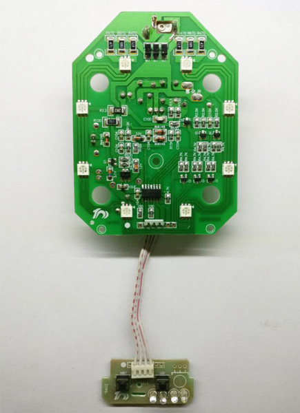
  • Complex process control for high-density boards: HDI and BGA assemblies demand precise equipment calibration, leading to higher defect rates without proper expertise.
  • Inadequate testing coverage: Certain board areas (e.g., component bottoms) are hard to inspect via AOI, leading to missed defects.
  • Delayed delivery due to design mismatches: Lack of DFM reviews leads to design changes mid-production, extending lead times and increasing costs.
Pain Points of PCB Assembly Services Switzerland, https://www.bestpcbs.com/blog/2026/02/pcb-assembly-services-switzerland/

One Stop Switzerland PCBA Service: Solving Supply Chain Delays Problems

Our one-stop Switzerland PCBA service eliminates supply chain delays primarily through integrated resource synergy and streamlined supply chain management, a core strength distinguishing our services. We have established a stable cooperative network with 15+ globally verified component suppliers and built a professional intelligent component warehousing center, stocking core electronic components commonly used in medical and industrial fields. This integrated resource layout avoids risks of component shortages and long international logistics cycles, shortening component sourcing lead time from 4-6 weeks to 3-5 days and fundamentally solving delays caused by material acquisition difficulties.

The comprehensiveness of our one-stop service ensures smooth supply chain operation by integrating pre-production DFM review, component verification, precision assembly, full-process testing, and timely delivery into a seamless process. We conduct professional DFM analysis before production to identify design mismatches that may cause mid-production modifications, avoiding delays from rework. Simultaneously, we utilize MES intelligent management systems for real-time tracking of production and logistics, dynamically adjusting production schedules based on order urgency to ensure each link is closely connected, enabling reliable on-time delivery even for urgent orders.

One Stop Switzerland PCBA Service, https://www.bestpcbs.com/blog/2026/02/pcb-assembly-services-switzerland/

Why Choose EBest(Best Technology) for PCB Assembly Services Switzerland?

Reasons why choose EBst(Best Technology) for PCB assembly services Switzerland:

  • 5-Year Quality Warranty: We provide a 5-year quality warranty for all our PCB assembly services Switzerland, covering manufacturing defects, soldering issues, and assembly-related component failures, offering free repair or replacement to minimize your post-delivery risks and ensure long-term product reliability.
  • Advanced MES Tracking System: Our advanced MES (Manufacturing Execution System) enables real-time tracking of the entire production process, from material incoming to final delivery, supporting end-to-end traceability of materials, processes and test data for easy compliance audits and production progress inquiry.
  • Strict Multi-Level Quality Inspection: We implement three-level quality inspection (incoming material inspection, in-process inspection, final inspection) using AOI, X-ray and functional testing equipment, ensuring a first-pass yield of 99.8% and eliminating defective products before delivery.
  • Rapid Prototype Turnaround: We offer fast prototype assembly with a 24-48 hour turnaround time and small-batch production delivery within 3-5 days, accelerating your product development cycle and helping you launch products to market faster.
  • Customized Assembly Solutions: We tailor assembly processes to your unique project needs, including ultra-miniaturized components (01005), high-temperature resistant PCBA (-55°C to 125°C) and HDI boards with 10μm line/space, adapting to diverse industry requirements.
  • Full Compliance Certifications: We hold ISO 9001:2015, ISO 13485:2016, and IPC-A-610 Class 3 certifications, fully meeting the strict compliance requirements of medical, industrial and high-reliability electronic fields in Switzerland.
  • Transparent Pricing & No Hidden Fees: We provide detailed, itemized quotes upfront, with zero setup fees for orders over 100 units, ensuring you have clear cost control without any unexpected additional charges.
  • Comprehensive Testing Services: We offer one-stop testing services including ICT, FCT, functional testing and reliability testing, verifying every PCB assembly’s performance and durability to avoid post-delivery failures.
  • Global Verified Supplier Network: We cooperate with 15+ globally verified component suppliers and operate an intelligent warehousing center, ensuring stable material supply and shortening sourcing lead times to 3-5 days.
  • 24/7 Dedicated Project Support: Our professional team is available 24 hours a day, 7 days a week to respond to your inquiries, update project progress and resolve any assembly-related issues promptly.

Types of PCB Assembly Services Switzerland We Offered

PCB Manufacturing Types

  • Rigid/Flexible/Rigid-Flex Boards: Supports sizes ranging from 50mm to 700mm × 460mm, suitable for industrial equipment and wearable electronics.
  • Custom Shaped Circuit Boards: Provides cutting of circular, rectangular, and non-transparent special-shaped PCBs to meet the needs of space-constrained applications such as medical equipment.

Production Service Modes

  • Small Batch Rapid Prototyping: Equipped with a real-time MES scheduling system, responding to production line bottlenecks within 1 hour to ensure timely delivery of urgent orders.
  • Medium to Large Volume Manufacturing: Coordinates component procurement through a local Swiss supply chain network (Zurich/Biel) to reduce logistics delay risks.

Value-Added Services

  • Design Engineering Support: Collaborates with institutions such as CSEM to provide signal integrity optimization, compatible with high-frequency applications in automotive electronics.
  • Full-Process Quality Monitoring: 100% production data traceability, compliant with ISO and CE certification standards.
  • Mechatronics Assembly: Extends to the integrated assembly of precision components (such as printer heating units).

Our Switzerland PCBA Capabilities

ItemCapabilities
Placer Speed13,200,000 chips/day
Bare Board Size0.2 x 0.2 inches – 20 x 20 inches/ 22*47.5 inches
Minimum SMD Component01005
Minimum BGA Pitch0.25mm
Maximum Components50*150mm
Assembly TypeSMT, THT, Mixed assembly
Component PackageReels, Cut Tape, Tube, Tray, Loose Parts
Lead Time1 – 5 days

Case Studies of Medical PCB Assembly Services Switzerland

Project Background: A Swiss medical device company sought a trusted partner for assembling PCBA for their new neurostimulator. Dissatisfied with their previous provider’s inconsistent quality and missed deadlines, they needed a reliable PCB assembly services Switzerland provider meeting strict medical device manufacturing standards.

Project Requirements: Key requirements included a 12-layer rigid-flex PCB assembly, ISO 13485:2016 compliance, 99.8% first-pass yield, 14-day delivery, 30μm line/space for high-density components, and FDA certification compatibility.

Project Challenges: Critical challenges included: ±100μm layer-to-layer alignment error causing intermittent signal failure (risking FDA failure); difficult placement of small 0201 components (prone to soldering defects); and strict biocompatibility requirements for all materials.

Our Solutions: Our solutions addressed these challenges: optical alignment closed-loop control reduced alignment error to ±50μm; high-precision SMT machines ensured accurate 0201 component placement; we sourced biocompatible, RoHS-compliant materials with MES traceability; and pre-production DFM reviews prevented potential issues.

Output Results: Exceptional results: 99.9% first-pass yield, 500 units delivered 2 days early, consistent ±45μm alignment error, zero FDA pre-certification non-conformities, and a 0.05% failure rate during 6-month field trials, demonstrating our reliable PCB assembly services Switzerland.

Case Studies of Medical PCB Assembly Services Switzerland, https://www.bestpcbs.com/blog/2026/02/pcb-assembly-services-switzerland/

FAQs of PCB Assembly in Switzerland

Q1: How can I ensure components used in Swiss PCBA are not counterfeit?​
A1: Partner with suppliers that provide full material traceability (batch IDs, certificates of conformity) and conduct incoming inspections using X-ray and optical testing. We verify all components against IPC standards and maintain a list of 15+ verified local suppliers to eliminate counterfeit risks.​

Q2: What is the typical lead time for PCB assembly services Switzerland?​
A2: Lead times vary by order size: prototypes (24-48 hours), small batches (10-100 units: 3-5 days), medium batches (100-1,000 units: 7-10 days), and large batches (1,000+ units: 10-14 days). Local component warehousing can reduce lead times by 30-40%.​

Q3: Is it cost-effective to use small-batch PCB assembly in Switzerland?​
A3: Yes, with our zero setup fees for orders over 100 units and optimized production processes, we reduce per-unit costs by 25% for small batches. We also offer flexible pricing for repeat small-batch orders to further lower costs.​

Q4: How do I ensure my PCBA meets Swiss medical device compliance standards?​
A4: Work with a provider certified to ISO 13485:2016 and experienced in medical PCBA. We conduct pre-production compliance reviews, use FDA-approved materials, maintain end-to-end traceability, and provide documentation required for CE and FDA certifications.​

Q5: What should I do if my PCB design has DFM issues for Swiss assembly?​
A5: Request a free DFM review before production. Our team identifies design mismatches (e.g., component spacing, pad size) within 24 hours and provides actionable adjustments to optimize for Swiss assembly processes, reducing rework and delays.

You may also like