PCB manufacturing PCB manufacturing
Home > Blog

What You Need to Know About Power Strip PCB Board?

January 9th, 2025

Power strip PCB board plays a vital role in power distribution, safety, and design. Power strips are an essential part of our daily lives, offering a simple way to power multiple devices from a single outlet. A Power Strip PCB Board plays a crucial role in this setup. In this blog, we will explore the power strip PCB board in depth, including its components, lifespan, and design, while highlighting the benefits it provides.

What is a Power Strip PCB Board?

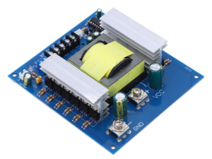
A Power Strip PCB Board is a printed circuit board (PCB) that serves as the backbone of a power strip. It connects the various components within the strip, ensuring proper power distribution to the connected devices. The PCB inside the power strip helps manage power flow, prevent overloads, and offers essential protection mechanisms for both users and appliances. This board is built with several copper traces that carry the current from the power source to each socket, allowing multiple devices to draw power simultaneously.

What Are the Components of a Power Strip?

A typical power strip is composed of several key components. These include the power PCB board, the sockets, the wiring, a surge protector, and a fuse. The PCB board is responsible for distributing power across each socket. The surge protector safeguards connected devices from voltage spikes. The fuse acts as a fail-safe, cutting off the power in case of an overload. All of these components work together to ensure safety and functionality, protecting your valuable electronics from potential damage.

What Is the Life Expectancy of a Power Strip?

The life expectancy of a power strip can vary depending on its quality and usage. Typically, a well-maintained power strip lasts between 3 to 5 years. However, this lifespan can be shorter if the strip is exposed to frequent power surges or overloaded. Regularly checking for wear and tear, like frayed wires or damaged sockets, is important to ensure that the power strip remains safe to use. A good quality PCB can help extend the life of the power strip, as it better handles power distribution and surge protection.

Why Do Power Strips Have 3 Prongs?

The three-prong design on power strips is a safety feature. The three prongs are made up of a live (hot) wire, a neutral wire, and a ground wire. The ground prong is crucial for ensuring that excess electrical current is safely diverted to the ground, reducing the risk of electric shock or fire. It’s a standard safety feature that helps protect both users and the devices plugged into the power strip.

What Is the 1363 Power Strip?

The 1363 power strip refers to a specific standard for power strips in some regions, particularly in New Zealand and Australia. It dictates the electrical safety features and configurations of the power strip, ensuring that it meets the safety requirements necessary for protecting connected devices. The standard typically covers the power rating, surge protection, and grounding methods, which are vital for ensuring that the power strip functions safely and effectively.

How Do I Identify a PCB Board?

Identifying a PCB board within a power strip is quite simple. The PCB is typically a flat board with a smooth surface and a series of copper traces. These traces connect various components like capacitors, resistors, and connectors, which are crucial for managing electrical flow. If you look closely, the board will also have markings or a part number that can help you trace the manufacturer and the specific design of the PCB. If you’re ever unsure about its authenticity or functionality, refer to the manufacturer’s manual for more details.

How to Design the Power Strip PCB Board?

Designing a power strip PCB board requires careful planning to ensure safety, reliability, and efficiency. The board design needs to handle high power loads, support various components like resistors, capacitors, and protection elements like fuses and surge protectors. The layout of the copper traces should minimize the risk of short circuits or power surges. Additionally, the PCB should be designed to accommodate the specific power rating and the number of outlets in the power strip. Using high-quality materials and following industry standards are key to ensuring the power strip performs well over time.

What Are the Benefits of the Power Strip PCB Board?

Power strip PCB boards offer several significant benefits that contribute to the performance and safety of the power strip. One major advantage is improved power distribution. A well-designed PCB ensures that power is evenly spread across all outlets, preventing any individual device from drawing too much current. PCBs also allow for better integration of protection features, such as surge protection and fuses, which guard against electrical hazards. Additionally, PCBs are compact, efficient, and cost-effective, allowing manufacturers to produce high-quality power strips at a reasonable price. Whether you need multiple types of PCB board products or a customized PCB board solution for manufacturing power strip. EBest Circuit (Best Technology) provides excellent service and fast delivery. For more information or any inquiry, warm welcome to reach out to us at sales@bestpcbs.com.

Power Strip PCB boards are essential to the design and functionality of power strips, offering efficient power distribution and safety features. Understanding the components, design process, and benefits of these boards helps in choosing the best power strip for your needs. Whether you’re designing one or purchasing a pre-made product, the role of the PCB inside is crucial to its overall performance and longevity. Choosing a power strip with a high-quality PCB ensures that your devices are always powered safely and reliably.

You may also like

What is 0.4mm thickness PCB? Ultrathin PCB

January 9th, 2025

What is 0.4mm thickness PCB? 0.4mm thickness PCB is an ultra-thin printed circuit board with a thickness of only 0.4 mm. This type of PCB has high requirements in design and manufacturing, because its thinness makes it easy to cause problems such as warping and deformation during processing. 0.4mm thickness PCB is usually used in electronic devices with strict requirements on space and weight. It can meet the development trend of miniaturization and thinness of modern electronic products.

What is 0.4mm thickness PCB? Ultrathin PCB

What is a 0.4mm Thickness PCB?

A 0.4mm thickness PCB refers to a printed circuit board with a thickness of 0.4 mm. ‌This thickness of PCB is generally considered to be the minimum thickness starting point for multi-layer PCB design, suitable for application scenarios that require highly integrated and compact design‌.

0.4mm PCB has the following characteristics:

  • Thin design‌: Suitable for electronic products that require highly integrated and compact design, such as smartphones, tablets and other portable devices.
  • High reliability: Due to its thin design, 0.4mm PCB performs well in complex wiring and fine design, and can provide stable electrical performance and mechanical strength.
  • ‌Cost-effectiveness‌: Although the manufacturing process is more complicated, the overall cost is relatively low because it uses less material.

0.4mm PCB is mainly used in the following fields:

  • Portable devices: Such as smartphones, tablets, wearable devices, etc., which require lightweight and powerful circuit boards.
  • High-density interconnect applications: In occasions where high integration and complex wiring are required, 0.4mm PCB provides a better solution.
  • Radio frequency identification (RFID) and smart cards: Such as RFID tags, IC cards, SIM cards, etc., these applications require circuit boards that are both thin and reliable.

What are the advantages of 0.4mm thickness PCB?

0.4mm thickness PCB has the following advantages:

  • Reduced material cost: Due to the use of less expensive materials such as copper, the material cost of 0.4mm thickness PCB is lower.
  • Compatibility with advanced technologies: PCBs of this thickness are compatible with advanced technologies such as laser direct imaging and can be used without damaging flexible circuits.
What is 0.4mm thickness PCB? Ultrathin PCB
  • High reliability: Ultra-thin PCBs can host custom repeatable routing paths, reduce rework, and have higher reliability.
  • Strong protection: The conductors on these PCBs have a polyimide cover layer to protect against a range of potentially harsh conditions, such as vibration and acceleration on the joints.
  • High durability: 0.4mm thick PCBs can withstand millions of bending cycles and are suitable for applications that require frequent bending.

In addition, 0.4mm thick PCBs are suitable for a variety of application scenarios, including RFID smart cards, IC cards, SIM cards, electronic tags, mobile phone charging modules, wearable devices, etc.

What are the disadvantages of 0.4mm thickness PCB?

The disadvantages of 0.4mm thickness PCB mainly include the following aspects:

  • Difficulty in manufacturing: Due to the thinness of 0.4mm thickness PCBs, they are easily affected by external factors during the manufacturing process, which increases the difficulty and cost of manufacturing.
  • Lower mechanical strength: Thinner PCBs are more likely to deform or be damaged when subjected to external forces, especially in environments with high-frequency vibration or mechanical shock, which may affect their stability and reliability.
  • Poor heat dissipation: Thinner PCBs have a relatively small heat dissipation area, which is not conducive to the rapid dissipation of heat, and may cause local overtemperature, affecting the stable operation of electronic components.
  • Increased welding difficulty: During the welding process, thinner PCBs are easily affected by the welding temperature, which may cause loose welding points or welding defects.
  • Signal transmission problems: Thinner PCBs may affect the integrity and transmission speed of signals due to the shorter signal path when transmitting high-frequency signals.

How to make 0.4mm thickness PCB?

There are many aspects to consider when making 0.4mm thickness PCBs.

1. Material selection

  • Substrate: Select a substrate suitable for 0.4mm thickness. Generally, 0.3mm raw materials are used to make 0.4mm PCB boards. The type of substrate is usually FR-4 or other materials suitable for thin boards.
  • Copper foil thickness: The thickness of the copper foil affects the conductivity and strength of the PCB. Common copper foil thicknesses include 1 ounce (about 35 microns), 2 ounces (about 70 microns), etc.

2. Production process

  • Cutting: Cutting large-sized copper foil boards into small pieces suitable for production.
  • Drilling: Drilling is the first process for the formal production of circuit boards, including electrical holes, mechanical holes, vias, etc. For 0.4mm thick PCBs, laser drilling may be required to achieve smaller apertures.
  • Lamination: By combining different core thicknesses and prepreg sheets, a finished PCB thickness of 0.4mm can be achieved.
  • Electroplated: Electroplated after drilling to ensure good conductivity in the hole.
  • Solder mask: Add a solder mask to the surface of the PCB to protect the copper wire from oxidation and prevent short circuits during welding.
  • Surface treatment: Common surface treatment methods include immersion gold, tin spraying, etc. to improve the conductivity and oxidation resistance of the PCB.

What are the difficulties in making a 0.4mm thick PCB?

The main difficulties in making a 0.4mm thick PCB include the following aspects:

  • Lamination difficulties: As the copper thickness increases, the line gap is deeper, and more resin filling is required, which increases the complexity and cost of processing.
  • Drilling difficulties: As the board thickness increases, the drilling difficulty increases. Thick copper boards are usually thicker than 2.0mm, and new knives and segmented drilling techniques are required to reduce the difficulty when drilling.
  • Thermal management: Due to the increase in power consumption of electronic devices, thermal management has become a key challenge. When designing, it is necessary to consider appropriate heat dissipation structures and heat dissipation component layouts to ensure that components work properly and avoid thermal damage.
  • ‌Signal integrity‌: High-frequency signals and high-speed digital signal transmission need to consider issues such as signal loss, impedance matching, and interlayer crosstalk.
  • ‌Electromagnetic compatibility (EMC) and electromagnetic interference (EMI): Measures need to be taken to reduce electromagnetic radiation and improve anti-interference capabilities.
  • Process and material selection: Choose the appropriate printing method and substrate material to ensure that the circuit board that meets the requirements is manufactured.

How to deal with the warping problem of 0.4mm thick PCB?

There are several ways to deal with the warping problem of 0.4mm thick PCB:

  • Choose high Tg board: Boards with higher Tg can withstand higher temperatures and reduce warping caused by temperature changes. Although the cost is higher, it can effectively resist high temperature deformation.
  • Reduce via restrictions: The via design in multilayer boards should be reasonable to avoid excessive restrictions on the cold expansion and contraction of the board and reduce warping.
  • Control temperature changes: Appropriately reduce the reflow temperature or slow down the heating and cooling speed to reduce the expansion and contraction of materials caused by temperature changes.
  • Use laser drilling technology: Laser drilling can reduce stress during processing and reduce the risk of warping.
  • Mechanical leveling: Use a flattening machine to mechanically level the PCB, which is suitable for PCBs with moderate warping.

The following aspects can be used to deal with the warping problem of 0.4mm thickness PCB:

What should I pay attention to when using 0.4mm thickness PCB?

The following points should be noted when using 0.4mm thickness PCB:

  • Trace spacing and width: On 0.4mm thickness PCB, the trace spacing is usually recommended to be no less than 0.2mm to ensure stable signal transmission and reduce interference. The trace width should be designed according to the current carried. Usually the width of the power line should be between 1.2~2.5mm, and the width of the signal line should be between 0.2~0.3mm.
  • Wiring rules: In high-density and high-precision PCB design, the line width and spacing are generally set to 0.3mm. If solder mask defined (SMD) pads are used, the thickness of the traces between the pads should be appropriately reduced to avoid the problem of pad lifting during soldering or desoldering.
What is 0.4mm thickness PCB? Ultrathin PCB
  • Heat dissipation and mechanical support: For devices with high power consumption, 0.4mm thick PCBs may not be enough to provide sufficient mechanical support and heat dissipation performance. For such devices, it is recommended to choose a thicker PCB to provide better mechanical support and heat dissipation performance.
  • Design details: When designing the PCB, it should be noted that the spacing between components should be greater than 0.5mm, and the spacing between the chip pins and peripheral devices should be greater than 1.0mm. In addition, the width of the ground line should be greater than the power line to ensure a stable current supply.

0.4mm thick PCB has become an ideal choice for modern electronic products such as smartphones and wearable devices due to its ultra-thin characteristics, meeting the development needs of miniaturization and thinness. However, problems such as warping are prone to occur during production. As a professional PCB manufacturer, BEST Technology has strong manufacturing strength to ensure that each 0.4mm thick PCB effectively reduces the occurrence of warping. If you have corresponding needs, please feel free to contact us at sales@bestpcbs.com!

You may also like

Why You Need Turnkey PCBA Assembly Service Right Now?

January 9th, 2025

Turnkey PCBA assembly service has become an essential part of the manufacturing industry, particularly in electronics. It provides a complete solution for companies needing printed circuit board assemblies (PCBAs) but lacking the resources or expertise to handle the intricate process themselves.

What is Turnkey PCB Assembly?

Turnkey PCB assembly is a full-service solution for the production of printed circuit boards (PCBs) and their assembly into functional electronic products. This service includes everything from designing the circuit boards to sourcing the components, assembling the PCBs, and delivering the final product. The term “turnkey” refers to a ready-to-use product, where you simply provide the specifications, and the service provider takes care of the rest.

In a typical turnkey PCBA assembly service, the manufacturer handles every step in the process, ensuring that the product meets the client’s requirements without the need for them to get involved in the details. This eliminates the need for multiple suppliers, reducing costs and saving time.

What Does Turnkey Mean in Manufacturing?

In manufacturing, turnkey refers to a complete solution where the service provider is responsible for every aspect of production. This includes design, sourcing materials, manufacturing, and testing. Once the project is completed, the product is ready for immediate use, hence the term “turnkey.” It offers simplicity for clients, as they can rely on a single supplier for all their manufacturing needs.

For PCB assembly, this means that the manufacturer will take care of everything from sourcing the necessary components to assembling and testing the final product. The client’s only responsibility is to supply the initial design or specification.

What is the Difference Between PCB and PCB Assembly?

A PCB (Printed Circuit Board) is a flat, rigid board used to mechanically support and electrically connect electronic components. It serves as the base for the circuit components that make up an electronic device, such as resistors, capacitors, and chips. The PCB itself does not perform any function until components are attached.

PCB assembly, on the other hand, refers to the process of placing and soldering these electronic components onto the PCB. The result is a complete, functional assembly, often called a PCBA (Printed Circuit Board Assembly). The assembly process involves precise placement, soldering, and testing of components to ensure the board works as intended.

What Specific Services Are Included in Turnkey PCBA Assembly Service?

A turnkey PCBA assembly service typically includes the following services:

1. PCB Design: If you don’t have a design yet, some providers offer PCB design services, creating the layout and schematic based on your specifications.

2. Component Sourcing: This includes purchasing all the components necessary for your project, ensuring they meet the required standards.

3. PCB Manufacturing: This is the process of producing the actual PCB, including layer stacking, etching, drilling, and other steps to create the board itself.

4. PCB Assembly: The components are placed on the PCB and soldered into place, often using automated machines for precision.

5. Testing and Inspection: Quality checks such as functional testing, X-ray inspection, and visual inspection ensure that the PCB is properly assembled and functional.

6. Packaging and Delivery: The final product is packaged and shipped to the client, ready for integration into the final product.

This comprehensive approach reduces lead times and ensures that clients receive a finished product that meets their expectations.

What is the Major Difference Between a Turnkey Project and a Design Build?

The primary difference between a turnkey project and a design build lies in the scope of responsibility.

Turnkey Projects: In a turnkey project, the service provider is responsible for every aspect of the project, from start to finish. The client hands over the specifications, and the provider handles design, procurement, manufacturing, and testing. Once completed, the product is ready for use.

Design Build Projects: In a design-build project, the client has more involvement. The service provider is typically responsible for the design and construction, but the client may still need to source components or provide additional input during the process. The client may need to manage more aspects of the project compared to a turnkey approach.

While both models aim to streamline production, turnkey projects are more hands-off for the client and typically offer greater convenience and efficiency.

What Files Are Needed for PCB Assembly?

To begin the PCB assembly process, several files are necessary. These files provide the information needed for manufacturing and assembling the PCB:

1. Gerber Files: These are the standard files for PCB design and detail the layers of the PCB, including copper layers, silkscreen layers, and soldermask layers.

2. Bill of Materials (BOM): A list of all the components required for the PCB assembly, including their specifications and quantities.

3. Pick-and-Place Files: These files contain precise information about where each component should be placed on the PCB, ensuring accurate placement during assembly.

4. Assembly Drawings: These drawings provide a visual reference for the assembly process, often showing where components should be placed.

5. Test Specifications: Details about the tests that need to be performed on the finished PCB to ensure quality and functionality.

These files ensure that every aspect of the production process is well-defined and can be accurately followed.

How Does PCB Assembly Work?

The PCB assembly process is a multi-step procedure that involves placing and soldering electronic components onto the PCB. The basic steps are as follows:

1. Component Sourcing: The required components are sourced and inspected for quality.

2. Solder Paste Application: Solder paste is applied to the PCB in areas where components will be placed.

3. Pick-and-Place: Using automated machines, components are placed precisely on the PCB.

4. Soldering: The PCB passes through a reflow oven, where the solder paste is melted and bonds the components to the board.

5. Inspection and Testing: The assembled PCB is inspected for errors and tested to ensure functionality.

6. Final Assembly: After testing, the board is packaged and shipped to the client.

Each step requires precision and attention to detail to ensure that the final product is functional and reliable.

What Are the Advantages of Turnkey Projects?

Turnkey projects offer several advantages that make them highly attractive, especially for businesses that want a hassle-free solution:

1. Simplified Process: The client only needs to provide initial specifications, with no need to worry about the intricacies of the manufacturing process.

2. Cost Efficiency: By bundling all services under one provider, turnkey solutions often result in lower costs, especially in terms of supply chain management and reduced overhead.

3. Time Savings: The provider handles all aspects of production, resulting in faster project timelines.

4. Quality Assurance: With a single provider responsible for all phases of production, consistency and quality are easier to maintain.

5. Focus on Core Competencies: Clients can focus on their product’s design and marketing while leaving the manufacturing details to the experts.

In short, turnkey PCBA assembly services offer a seamless, efficient, and reliable way to get your PCBs assembled and ready for integration into your electronic products.

Turnkey PCBA assembly services provide a comprehensive solution that simplifies the process of getting your PCBs designed, assembled, and ready for use. With services ranging from component sourcing to final delivery, it offers businesses a one-stop shop for all their assembly needs. By choosing a turnkey provider, companies can enjoy cost savings, faster timelines, and a hassle-free manufacturing experience. EBest Circuit (Best Technology) provides turnkey PCBA assembly service, delivering high-quality products with quick turnaround times. If you’re interested in our turnkey PCBA assembly service, feel free to contact us at sales@bestpcbs.com for more information.

You may also like

How to copy PCB board? PCB reverse engineering

January 8th, 2025

How to copy PCB board? PCB reverse engineering. First, get the PCB sample to be copied, then disassemble and record the component information on the sample to make a BOM table; then scan the sample to get its PCB layout image; then trace the routing and place the components according to the image to complete the drawing of the PCB diagram; finally, use the drawn PCB diagram to make a new PCB board, solder the corresponding components, and test and debug to ensure normal function.

How to copy PCB board? PCB reverse engineering

What is copy PCB?

PCB copying, also known as circuit board cloning, refers to the reverse analysis of the circuit board through reverse research and development technology on the premise of existing electronic products and circuit boards, restoring the original product’s PCB files, bill of materials (BOM), schematic files and other technical files, and using these technical files to make PCB boards, solder components, test and debug, and finally complete the complete copy of the original circuit board sample.

How to copy PCB?

The process of copying PCB can be divided into the following points:

1. Get the PCB board to be copied and scan and back it up, remove the components and record the information to make a BOM table, and clean the residue on the surface of the PCB board.

2. Scan the cleaned PCB board, import it into the copy board software, draw the routing and place the components according to the image, and export the PCB file.

3. Make the PCB file into a PCB board, test and debug after soldering the components, and ensure that the copied PCB board functions normally.

What are the steps to copy PCB?

The process of copying PCB can be divided into the following steps:

1. Preparation

  • Get the PCB board: First, you need a PCB board, which can be provided by the customer or available on the market.
  • Scan and back up: Scan and back up the PCB board for reference during the copying process.

2. Remove components

  • Remove components: Use tools such as hot air guns to remove components on the PCB board, pay attention to temperature control, and avoid damaging components or PCB.
  • Make a BOM table: Record the model, parameters, location and other information of the removed components, and make a bill of materials.

3. Clean the PCB board

  • Remove residues: Clean the tin slag and other residues on the surface of the PCB board after the components are removed.

4. Copy board

  • Scan the PCB board: Scan the cleaned PCB board again to obtain a clear image.
  • Import the copy board software: Import the scanned image into the copy board software.
  • Draw the routing and place components: In the copy board software, draw the routing of the PCB according to the scanned image and place the corresponding components.
  • Export PCB file: Export the drawn PCB design to PCB file format.
How to copy PCB board? PCB reverse engineering

5. Make and test

  • Make PCB board: Make the exported PCB file into a PCB board.
  • Weld components: Weld the purchased components to the made PCB board.
  • Test and debug: Test and debug the welded PCB board to ensure its normal function.

Notes:

  • Legal compliance: When copying PCB, you need to pay attention to relevant laws and regulations to avoid infringement of intellectual property rights.
  • Precision control: During the scanning, drawing and production process, the precision must be strictly controlled to ensure that the copied PCB board is consistent with the original board

Does copy PCB comply with regulations?

Whether the copy PCB complies with regulations depends mainly on the purpose of the copy and whether the relevant intellectual property laws are complied with.

  • Intellectual property respect: The intellectual property rights of the original design must be respected when copying the PCB.
  • Legality of reverse engineering: In some cases, copying PCBs through reverse engineering is allowed, but the premise is that such behavior must be used for legitimate purposes.

In summary, whether the copying of PCBs is legal depends mainly on the purpose of the copying and whether the corresponding intellectual property license has been obtained. If it is for commercial purposes and without permission, it may violate relevant laws and regulations and face legal risks.

What are the benefits of copying PCB?

The benefits of copying PCBs mainly include the following aspects:

  • Save time and cost: By copying PCBs, companies can avoid the high cost and time cost of designing from scratch. Especially in urgent and complex projects, it can significantly save time and manpower.
  • ‌ Improve R&D efficiency: Copying PCBs can accelerate the product R&D process, shorten the product R&D cycle, and enable products to be brought to market faster.
How to copy PCB board? PCB reverse engineering
  • Optimize performance and function: Copying PCB is not just a simple copy. Through the analysis and research of technical data, product performance and function can be optimized, thereby enhancing the market competitiveness of products.
  • Avoid intellectual property issues: By copying PCB, enterprises can avoid infringing on the intellectual property rights of others under the premise of legality.

What should I pay attention to when copying PCB?

The following points should be noted when copying PCB:

  • Back up the original file: Before starting to copy, be sure to back up the original PCB file and GERBER file.
  • Strict file operation: During the copying process, the PCB board must be remade strictly in accordance with the content in the GERBER file, and it cannot be modified at will.
  • Check the file content: After exporting the GERBER file, you need to carefully check the file content to ensure the accuracy of the copy board content.
  • ‌Processing inner layer circuits: When processing the inner layer circuits, since there are only copper foil and inner circuits, the actual circuits cannot be seen, and the inner layer circuits need to be checked through the outer layer circuits.
  • Copper plating: When plating copper, the copper foil and the inner circuit connection need to be disconnected to avoid connection with the outer circuit.
  • Proofread with CAM software: After the design is completed, use CAM software for proofreading to ensure the accuracy of the copy board content.
  • Record component information: Before copying, record the model, parameters and position of all components in detail, especially the direction of diodes and transistors and the direction of IC gaps.
  • Disassemble and clean the PCB board: Remove all components, clean the PCB board, clean it with alcohol, dry it, and put it in the scanner.
  • Image processing: Adjust the contrast and brightness to make the parts with and without copper film have a strong contrast. Remove noise, scratches, etc.
  • Generate PCB file: Convert the processed image to PROTEL format file, import it in PROTEL and compare whether the PAD and VIA positions are accurately overlapped.
  • Merge and verify: Import TOP.PCB and BOT.PCB in PROTEL and merge them into a complete PCB diagram. Use a laser printer to print the TOP layer and BOTTOM layer on a transparent film at a 1:1 ratio, and compare it with the original PCB to ensure that there is no error.

How does BEST Technology copy PCB?

As a professional PCB manufacturer, BEST Technology has the following process for copying PCB:

1. Submit sample photos

  • Customer operation: Please take clear photos of the PCB samples, including the component layout and routing details on both sides, and then send the photos to our email: sales@bestpcbs.com
  • Notes: Make sure the photos are clear enough to clearly show the component model, location and routing on the PCB board so that our engineers can conduct preliminary analysis and evaluation.
How to copy PCB board? PCB reverse engineering

2. Preliminary quotation and communication

  • Engineer evaluation: After receiving the sample photos, our engineers will give a rough copy price based on factors such as the complexity of the PCB in the photos, the number and type of components, etc.
  • Program and IC information: If the PCB contains a program IC, you need to inform us or provide a clear photo of the IC so that we can evaluate the difficulty and cost of program cracking and give a more accurate quotation.

3. Confirm the price and send samples

  • Price confirmation: After receiving our preliminary quotation, if you have any questions or need to adjust, you can communicate with us further until both parties reach an agreement on the price.
  • Sample delivery: After the price is determined, you need to send us PCB samples, preferably 2 samples, so that we can conduct more detailed analysis and cloning. After receiving the samples, we will provide you with an accurate quotation based on the actual sample situation.

4. Payment and production start

  • Payment process: After you confirm that the final quotation is correct, you will complete the payment according to our payment method.
  • Production start: After receiving the customer’s payment, we will officially start the PCB cloning work, including sample analysis, component disassembly, PCB drawing and other steps.

5. Provide design files and manufacture circuit boards

  • Design file delivery: After completing the copy board work, we will send you the complete Gerber file, schematic diagram and BOM (Bill of Materials) for your review and confirmation.
  • Circuit board manufacturing: After confirming that the design files are correct, we will start to manufacture circuit boards for you based on these files to ensure that the quality and performance of the circuit boards meet your requirements.

In summary, every step of the PCB copy process is meticulous to ensure that the copy board accurately restores the original board function. At the same time, it is very necessary to find a qualified PCB manufacturer. BEST Technology has rich experience in PCB manufacturing. If you have PCB copy needs, please feel free to contact us at sales@bestpcbs.com.

You may also like

What is Vias Plugged PCB and Why is It Important?

January 8th, 2025

Vias Plugged PCB has become a common technique to improve the integrity and functionality of a board in the world of PCB (Printed Circuit Board) manufacturing. This process involves filling or sealing the holes, known as vias, which are used to create electrical connections between different layers of a PCB. But why is via plugging so important, and what does it involve? In this blog, we’ll dive into what via plugging is, the different types of vias, and its role in PCB design and performance. Let’s explore the various aspects of this technique and its significance in the world of PCB production.

What is Via Plugging in PCB?

Via plugging is the process of filling or sealing vias, which are holes drilled into a PCB to establish electrical connections between different layers. These vias can be plugged for various reasons, such as preventing unwanted signals from traveling through the vias or ensuring better protection against environmental factors like moisture. The plugging material used may vary, but most commonly, it’s a resin, green oil, or solder mask. The plugged vias add structural integrity to the PCB and enhance its electrical performance.

What Are the Different Types of Vias in PCB?

PCBs can have several types of vias, each designed for specific purposes. The main types include:

Through-hole Vias: These are the most common vias, which pass through the entire board and connect all the layers.

Blind Vias: These connect an outer layer to one or more inner layers but do not pass through the whole PCB.

Buried Vias: These are located entirely within the PCB and do not reach the outer layers, offering a more compact design.

Micro Vias: Smaller than standard vias, they are used in high-density interconnects (HDI) PCBs to create intricate circuits.

Each type of via has its own purpose and is selected based on the design requirements of the PCB.

What’s the Purpose of Vias in PCB?

Vias serve several critical functions in PCB design. Their primary purpose is to provide electrical connections between different layers of the board. This allows signals to travel between top, bottom, and inner layers, creating complex and multi-layer circuits. Vias are also essential for thermal management, helping to dissipate heat across the PCB, ensuring it operates efficiently and remains within temperature limits.

What is the Difference Between Via Plug and Via Fill?

While both processes involve filling vias, they are slightly different in their application. Via plugging refers to sealing the via to prevent signal interference or to fill the via with a non-conductive material, such as resin or solder mask. Via filling, on the other hand, is typically done with a conductive material to ensure that the via still maintains an electrical connection, especially in high-frequency or high-performance PCBs.

What is the Difference Between Tented Via and Untented Via?

A tented via is a via that is sealed with a solder mask over the hole to protect it from environmental damage. This method is often used to prevent moisture or contaminants from entering the via. On the other hand, an untented via remains open and unsealed. Tented vias are commonly used in consumer electronics where the environment is relatively controlled, while untented vias may be seen in applications where electrical continuity is more critical than protection.

What is the Difference Between a PCB Hole and a Via?

The primary difference between a PCB hole and a via lies in their function. A PCB hole is simply a hole in the board, often used for mechanical purposes, such as mounting or securing components. A via, however, is specifically designed for electrical connections between the different layers of the PCB. While holes can be part of a PCB design, vias play a much more specific and functional role in the overall circuit design.

Do Vias Increase PCB Cost?

Yes, vias can increase the cost of manufacturing a PCB. The more complex the via design (e.g., blind or buried vias), the higher the cost due to the additional drilling and processing required. Moreover, the use of via plugging materials, such as resins or green oil, also adds to the cost. However, despite the cost increase, vias are often necessary for high-performance PCBs, especially those used in complex electronics, where the design requirements outweigh the cost considerations.

When to Use Vias in PCB?

Vias are used in PCBs when there’s a need for multi-layered designs or when connecting different electrical components across multiple layers is required. They are often used in high-density and high-frequency PCBs, such as those found in smartphones, computers, and medical devices. If you are designing a PCB that needs to be compact but complex, vias will be essential for providing the necessary electrical connections without compromising space.

Via plugging is an essential process in PCB manufacturing that contributes to both the functionality and durability of the board. Whether you’re working with through-hole, blind, buried, or micro vias, plugging them at the right time and with the right materials ensures that your PCB will perform optimally. By understanding the different types of vias and how they contribute to the overall design, you can make more informed decisions about when and how to use them in your PCB projects.

At EBest Circuit (Best Technology), we specialize in high-quality PCB manufacturing, offering a range of solutions for your project needs. From via plugging to precision design, we ensure that every PCB we produce meets the highest standards of performance and reliability. If you’re looking for a trusted partner for your PCB needs, reach out to us today at sales@bestpcbs.com!

You may also like

What Makes FR4 4 Layer PCB Ideal for Modern Electronics?

January 8th, 2025

FR4 4 layer PCB is a crucial component in modern electronics, offering a blend of durability, reliability, and efficiency. Built using flame-retardant FR4 material, these multilayer boards are designed to handle complex circuits while maintaining excellent performance. Their unique structure, with multiple conductive and insulating layers, supports advanced applications in high-speed and high-density designs. This blog explores the features, structure, and benefits of FR4 4-layer PCBs, answering key questions to provide a clear understanding of their role in electronic manufacturing.

What is FR4 PCB?

FR4 PCB refers to a printed circuit board made from a material called FR4. This material is a type of fiberglass-reinforced epoxy laminate that is widely used in the electronics industry. Its name, FR4, stands for “Flame Retardant 4,” which indicates its excellent fire-resistant properties. FR4 is highly valued for its strength, lightweight nature, and ability to withstand high temperatures. These qualities make it ideal for manufacturing PCBs, which serve as the backbone of electronic devices.

FR4 is not just a material; it is the standard for most PCB substrates. Its insulating properties help protect circuits from electrical interference, while its rigidity provides stability to the board. In the world of electronics, FR4 has become synonymous with reliability and performance.

Is FR4 Electrically Conductive?

No, FR4 is not electrically conductive. It is an insulating material, which is one of its most critical features. This non-conductive nature allows it to act as a barrier between different layers of a PCB, ensuring that electrical signals remain confined to their intended paths. This property is essential for preventing short circuits and signal interference.

The non-conductive nature of FR4 ensures that it can be used in multilayer PCBs without compromising performance. Manufacturers rely on its insulating capabilities to create intricate designs that support complex electronic systems. Its ability to maintain electrical isolation while providing mechanical support makes it indispensable in the industry.

What is a 4-Layer PCB?

A 4-layer PCB is a type of multilayer printed circuit board that consists of four distinct layers of conductive material. These layers are separated by insulating materials like FR4 and are laminated together to form a single board. The typical structure includes two outer layers and two inner layers, each serving specific purposes such as signal transmission, grounding, or power distribution.

4-layer PCBs are commonly used in devices that require compact designs and advanced functionality. They provide enhanced performance compared to single-layer or double-layer PCBs, making them suitable for high-speed circuits and applications with stringent space constraints. Their structure allows for efficient routing, reduced electromagnetic interference, and improved overall performance.

What is a 4-Layer PCB Structure?

The structure of a 4-layer PCB is carefully designed to optimize performance and functionality. Typically, the layers are arranged as follows:

Top Layer (Signal Layer): This is where most of the components are mounted, and primary signal routing occurs.

Inner Layer 1 (Ground Plane): Dedicated to grounding, this layer helps reduce noise and electromagnetic interference.

Inner Layer 2 (Power Plane): This layer is used for power distribution, ensuring consistent voltage levels across the board.

Bottom Layer (Signal Layer): Similar to the top layer, this is used for additional signal routing and component placement.

The separation of power and ground layers helps in maintaining signal integrity and minimizing interference. The insulating layers, often made of FR4, ensure electrical isolation between the conductive layers, enabling reliable and stable operation.

How Thick is 4 Layers of PCB?

The thickness of a 4-layer PCB can vary depending on its design and application. Generally, the total thickness ranges from 0.4mm to 3.2mm. The most common thickness for standard 4-layer PCBs is around 1.6mm, which balances durability and flexibility.

The choice of thickness depends on factors such as the number of components, the complexity of the circuit, and the intended use of the board. Thicker boards offer more mechanical strength, while thinner boards are suitable for compact devices. The use of FR4 as the core material ensures that even thin boards maintain their rigidity and reliability.

What is the Standard Thickness of a Copper Layer on a PCB?

The standard thickness of a copper layer on a PCB is typically measured in ounces per square foot. For most 4-layer PCBs, the standard copper thickness is 1 ounce per square foot, which translates to approximately 35 microns. However, depending on the application, this thickness can be increased to 2 ounces or more for high-current designs.

Copper thickness plays a crucial role in determining the current-carrying capacity and thermal management of the PCB. Thicker copper layers are often used in power distribution layers to handle higher currents, while thinner layers are sufficient for signal transmission.

How to Route a 4-Layer PCB?

Routing a 4-layer PCB requires careful planning and adherence to design principles. The process typically involves the following steps:

Define Layer Functions: Assign specific roles to each layer, such as signal routing, grounding, or power distribution.

Use Ground and Power Planes: Dedicate inner layers to ground and power planes to reduce noise and improve signal integrity.

Minimize Crosstalk: Maintain adequate spacing between traces to prevent signal interference.

Optimize Trace Widths: Ensure trace widths are appropriate for the current-carrying requirements.

Follow Design Rules: Adhere to industry standards and guidelines to ensure manufacturability and performance.

Software tools like PCB design software can assist in creating efficient layouts. By carefully considering the layer stackup and routing strategy, designers can achieve optimal performance and reliability.

Why is FR4 Used in PCBs?

FR4 is widely used in PCBs because of its exceptional properties. It offers high mechanical strength, excellent thermal stability, and reliable electrical insulation. These qualities make it suitable for a wide range of applications, from consumer electronics to industrial machinery.

Its lightweight nature and ease of fabrication further contribute to its popularity. FR4 can withstand high temperatures and resist moisture, ensuring durability in harsh environments. Moreover, its cost-effectiveness makes it an attractive choice for manufacturers, enabling them to produce high-quality PCBs without significantly increasing costs.

In conclusion, FR4 remains a cornerstone material in PCB manufacturing due to its unmatched combination of performance, reliability, and affordability. Its versatility ensures that it will continue to play a pivotal role in the advancement of electronic technologies. At EBest Circuit (Best Technology), we pride ourselves on delivering multiple types of FR4 4 layer PCB products that meet your high-quality standards while maintaining fast delivery times. For more information or any inquiry, warm welcome to reach out to us at sales@bestpcbs.com.

You may also like

PCB Multilayer Circuit Board: 17 multi layer boards

January 7th, 2025

The 17 multi layer boards is a highly integrated electronic component that alternately stacks 17 conductive layers and insulating layers and uses advanced interlayer connection technology (such as vias) to achieve electrical connection between the layers. Connections can significantly increase the wiring density and complexity of circuits. This design makes the 17 multi layer boards has broad application prospects in high-performance electronic equipment and can meet the strict requirements of these equipments for signal transmission speed, stability and functional diversity.

PCB Multilayer Circuit Board: 17 multi layer boards

What is a multi-layer circuit board?

The basic structure of a multilayer circuit board includes multiple conductive layers and insulating layers. The conductive layer usually uses copper foil or metallized holes, and the insulating layer is usually made of materials such as epoxy resin. Each layer is electrically connected through via holes, which are usually processed by drilling, laser drilling or chemical etching.

Advantages of multilayer circuit boards

  • High wiring density: Multi-layer circuit boards can achieve more complex wiring in a limited space to meet the needs of high-density electronic equipment.
  • Good electromagnetic shielding effect: The multi-layer design can effectively reduce electromagnetic interference and improve the stability and reliability of the system.
  • Low signal transmission delay: Multi-layer circuit boards reduce signal transmission delay and improve system performance by optimizing wiring and signal paths.
  • Suitable for complex systems: Multi-layer circuit boards are suitable for electronic devices that require a high degree of integration and complex functions, such as smartphones, tablets, etc.

How to make 17 multi layer boards?

The detailed steps for manufacturing a 17 multi layer boards are as follows:

  • Raw material preparation: Choose high-quality copper-clad laminates as raw materials. Commonly used copper-clad laminates include epoxy glass cloth substrates, etc.
  • Cutting: Use an automatic cutting machine to cut large-sized copper clad laminates into specific substrate sizes suitable for production needs.
  • Drilling: Use a CNC drilling machine to accurately drill holes at predetermined positions on the copper clad board.
  • Copper deposition: Copper ions in the electrolyte are deposited on the hole walls through electrochemical methods to form a uniform copper foil layer.
  • Dry film exposure and development: Use dry film for exposure and development, and use strong ultraviolet light to polymerize the dry film to form a preliminary cured circuit pattern.
  • Electroplating: In the electroplating production line, a layer of copper is plated on the exposed lines and hole walls through electrochemical reaction, and then a layer of tin is plated on the surface of the copper layer to protect the copper foil of the lines and hole walls from being eroded by the etching liquid.
  • Stripping and etching: Place the PCB in the stripping equipment, use stripping agent and cleaning methods to remove the remaining dry film, exposing the copper foil that is not protected by tin plating. Then use an etching solution to etch away the exposed copper foil, retaining the copper foil under the tin plating layer, and finally obtain the circuit pattern and metallized holes required for the design.
  • Inner layer process: Compared with single and double panels, the manufacturing of multi-layer boards has an additional inner layer process. Controlling the lamination process of the inner layers is critical to the electrical performance of controlled impedance transmission lines. The copper in the inner layer should be evenly distributed on the symmetrical layer to ensure balanced thermal stress during heating and avoid circuit board warping.
  • Laminated lamination: By combining different specifications of prepreg and copper-clad laminate (core board), all required thicknesses are achieved. The individual layers must be symmetrical and have the same layer thickness. After the lamination is completed, precise inter-layer adjustment and positioning are performed to ensure good adhesion between the inner layer and the prepreg.
  • Inspection: Circuit graphics are inspected using an automated optical inspection (AOI) system to ensure consistency of internal layers with CAD data and repair any connections or other defects found.

Through the above steps, a high-quality 17 multi layer boards can be manufactured.

When to use 17 multi layer boards?

1. High-frequency and high-speed signal processing scenarios

In communication base station equipment, such as the baseband processing unit (BBU) of a 5G base station. 5G signals have high frequency, large bandwidth, and extremely fast signal transmission speed. The 17 multi layer boards can efficiently route high-frequency, high-speed signals.

It can make the distance between the signal layer and the reference plane (ground layer) closer by reasonably arranging the positions of the signal layer, ground layer, and power layer, thereby reducing the loop inductance of the signal and reducing signal reflection and attenuation.

PCB Multilayer Circuit Board: 17 multi layer boards

And some inner shielding layers can be used to isolate signals in different frequency bands or sensitive signals from interference sources to ensure the integrity and accuracy of signal transmission.

For the communication line between the graphics processing unit (GPU) and the central processing unit (CPU) in high-speed computer systems. When performing large-scale graphics rendering or complex data operations, the data transfer rate is extremely high.

The 17 multi layer boards can provide enough wiring space to route high-speed differential signal pairs (such as PCI-Express interface signals) on different inner layers. At the same time, a complete ground plane is set up around it as a shield to reduce electromagnetic interference and ensure high speed. signal quality.

2. Complex circuit function integration

In the electronic control part of advanced medical equipment such as magnetic resonance imaging (MRI) equipment. MRI equipment contains complex radio frequency transmitting and receiving circuits, gradient magnetic field control circuits, image acquisition and processing circuits and other functional circuits. The 17 multi layer boards can distribute these circuits with different functions on different layers and connect them through vias.

In the controller of industrial robots, it needs to integrate multiple functions such as motion control, sensor signal processing, communication interfaces, and power management. The 17 multi layer boards allows the circuits of these functional modules to be reasonably distributed on each layer, making the layout of the circuit board more compact.

3. Special power and grounding requirements

In high-precision test and measurement instruments, such as spectrum analyzers. This type of instrument has extremely high requirements on the purity and stability of the power supply. The 17 multi layer boards can be equipped with multiple independent power layers, and decoupling capacitors are reasonably arranged between the power layer and the ground layer to form a low-pass filter network to effectively filter out power supply noise.

At the same time, through reasonable ground layer design, low-impedance ground paths are provided for different circuit modules to reduce the impact of ground bounce noise on measurement accuracy.

Active power filters (APF) in power electronic equipment. APF needs to process a large number of power signals and plays a key role in improving power quality. The 17 multi layer boards can provide suitable power and ground planes for different power conversion circuits and control circuits.

What are the disadvantages of 17 multi layer boards?

The disadvantages of 17 multi layer boards mainly include the following aspects:

  • 1. High cost: Due to the large number of layers and the complex manufacturing process, which requires more materials and finer processes, the cost is relatively high.
  • 2. Design is difficult: Designing a 17-layer PCB requires more factors to be considered, such as inter-layer connections, signal integrity and electromagnetic compatibility, etc. This requires higher professional skills from the designer and the design cycle may also be longer.
  • 3. Long production cycle: The production of multi-layer PCB involves multiple processes, such as lamination, drilling, copper plating, etc. These processes take time to complete, so the production cycle is relatively long.
  • 4. Difficulty in maintenance: Due to the complex internal structure, once a fault occurs, it is relatively difficult to locate and repair the problem, and sometimes even requires complete replacement.
  • 5. High requirements for design and manufacturing processes: more advanced equipment and technology are needed to ensure the quality and performance of multi-layer boards.

These shortcomings make 17 multi layer boards a reasonable trade-off between performance and cost in some applications.

How many layers can a circuit board have?

The number of layers in a circuit board can vary from single layer to multiple layers. Common layers include single layer, double layer, four layer, six layer, eight layer, ten layer, etc. High-end PCB boards can even reach 32 layers or more.

Application scenarios for different layers

  • Single-layer board: Suitable for simple circuit design, usually used in low-complexity electronic devices.
  • Double-layer boards: Suitable for medium-complexity designs that can accommodate more components and connections.
  • Four-layer board: Commonly used in designs that require better signal isolation and noise suppression, such as high-frequency circuits.

The manufacturing process of multilayer boards is very complex and requires more precise design and high-end processing technology. The more layers there are, the higher the manufacturing difficulty and cost. Therefore, when designing a circuit board, it is necessary to consider the circuit direction, number of layers, and materials to ensure the performance and reliability of the circuit board.

How many layers of circuit boards can we make?

With the continuous advancement of electronic technology, we are able to produce PCBs with more layers. Currently, FR4 PCBs with 20 to 32 layers can be realized. This high-level PCB structure provides engineers with greater design flexibility, allowing them to lay out various traces on different layers to meet different functional requirements.

Layers can be dedicated for power distribution, signal transmission, electromagnetic interference (EMI) shielding, and assembly of components. In order to effectively manage the number of layers, buried holes and blind holes are often designed in multi-layer PCBs to optimize circuit layout and signal transmission paths.

PCB Multilayer Circuit Board: 17 multi layer boards

For PCBs with more than 8 layers, high Tg FR4 materials are usually more popular than ordinary Tg FR4 because high Tg materials can maintain stable electrical performance and mechanical strength at higher temperatures, which is especially important for high-performance electronic devices. However, the increase in the number of layers also makes the PCB manufacturing process more complex and difficult, leading to higher costs.

In summary, we found that the 17 multi layer boards has significant advantages in signal integrity and space utilization, and can meet the needs of high-density electronic equipment, but its complex manufacturing process also brings higher costs and Production difficulty.

As a professional PCB manufacturer, BEST Technology has advanced production equipment and rich production experience, able to efficiently produce high-quality multi-layer PCB boards to meet customer needs for high-performance electronic equipment. Please feel free to contact us at sales@bestpcbs.com, we will provide a full range of services from design to production to ensure that every PCB board meets your strict standards.

You may also like

PCB Multilayer Circuit Board: pcb panel v-cut vs stamp hole

January 7th, 2025

V-CUT cuts a V-shaped groove on the PCB board, so that the board can be easily separated in subsequent processing, while the stamp hole sets a small hole on the edge of the board, making the board more neat and stable when separated, which can provide higher space utilization and better signal transmission performance. The combination of these two technologies not only improves production efficiency, but also ensures product quality and reliability.

PCB Multilayer Circuit Board: pcb panel v-cut vs stamp hole

What is PCB V-CUT?

PCB V-CUT is a technology that cuts a V-shaped groove on a printed circuit board, which is mainly used to facilitate subsequent board separation operations. V-CUT is to cut a series of V-shaped cuts on the PCB board and then break the board after applying appropriate force, thereby dividing the multilayer PCB into separate panels.

The role and importance of V-CUT

  • Improve manufacturing efficiency: In mass production, V-CUT can quickly divide large boards into multiple small panels to meet the needs of mass production.
  • Reduce material waste: Through V-CUT cutting, raw materials can be maximized, waste generation can be reduced, and production costs can be reduced.
  • Convenient assembly: V-CUT allows the separated small panels to be easily assembled and welded, improving production efficiency.

V-Cut is widely used in the batch manufacturing of multi-layer PCBs, especially when a large board needs to be divided into multiple small panels.

What are the advantages and disadvantages of V-Cut?

Advantages of V-Cut:

  • Easy to operate: The V-Cut design can facilitate the separation of SMT circuit boards after assembly, avoiding PCB bending and damage to electronic components that may be caused by manual separation.
  • Improve production efficiency: When assembling the edges of two boards, the efficiency of SMT patch lines and wave soldering can be significantly improved.
  • Wide range of applications: V-Cut is suitable for regular PCB boards, especially in batch production, the use of V-Cut can significantly improve production efficiency.

Disadvantages of V-Cut:

  • Can only cut straight lines: V-Cut can only cut straight lines, and it can only cut straight lines from one end to the end, and cannot be changed in the middle. If there is a 90-degree or other angle bend in the middle, it is not allowed.
PCB Multilayer Circuit Board: pcb panel v-cut vs stamp hole
  • High requirements for tools: The material and manufacturing process of V-Cut knives have a great influence on the cutting effect. For example, high-speed tool steel V-Cut knives are not wear-resistant and need to be frequently changed and sharpened, which affects production efficiency; alloy-inlaid V-Cut knives increase the brittleness of the blade due to welding, and the quality is difficult to guarantee, and the tooth breakage rate is high.
  • Restrictions on PCB thickness: PCB boards that are too thin or too thick are not suitable for V-Cut, because too thin boards are easy to break and too thick boards are difficult to cut.

What is a stamp hole?

A stamp hole refers to a hole on the motherboard panel that is used to connect small PCBs that make up the array together and to easily remove components from the PCB. Stamp holes are perforated, and when pushed down, the holes break, allowing components to be removed without damaging the PCB itself.

The specific functions of stamp holes include:

  • Connecting small PCB boards: When there are multiple small PCBs that need to be connected and connectors cannot be used, they can be connected through stamp holes. Perforations allow current to flow through the PCB and connect with other nearby PCBs.
  • Transmit power and data: Stamp holes can transmit power and data between two different PCBs or devices to achieve communication between devices.

Design requirements for stamp holes include:

  • Number of holes: Usually stamp holes are in groups of 5 to connect components together, but the specific number may vary depending on the PCB design.
PCB Multilayer Circuit Board: pcb panel v-cut vs stamp hole
  • Size: The size of stamp holes is usually 0.020 inches or 0.5 mm in diameter, and the specific size will vary depending on the PCB design.
  • Hole spacing: The spacing of stamp holes is usually 0.030 inches or 0.76 mm to prevent components from being too close and causing short circuits.

In addition, design tips for stamp holes include:

  • Sufficient pull tabs: In order to maintain the integrity of the PCB, the pull tabs should be strong enough to support the weight of the components above.
  • Stay away from sensitive components: Stamp holes should be away from sensitive components to avoid electrical short circuits caused by damage to the pull tabs.
  • Spacing: The spacing between two stamp holes should be between 60mm-90mm to facilitate the installation of components.

What are the advantages and disadvantages of stamp holes?

The advantages of stamp holes include:

  • Improved production efficiency: Stamp holes can connect multiple small-sized PCBs together for production and processing, thereby simplifying the production process and reducing costs.
  • Convenient assembly and disassembly: In situations where detachable connections are required, such as modular designs, stamp hole connections can achieve convenient assembly and disassembly, facilitating product repair and upgrades.
  • Reduced space occupation: The stamp hole design can greatly reduce the required space, especially suitable for compact designs.
  • Improved signal transmission performance: Stamp holes shorten the signal path, reduce signal delay and cross interference, and are suitable for complex multi-layer board designs.
PCB Multilayer Circuit Board: pcb panel v-cut vs stamp hole

Disadvantages of stamp holes include:

  • Possible cost increase: The design of stamp holes will increase certain costs because holes need to be reserved on the PCB, and the size of these holes will also be included in the overall size of the PCB.
  • The broken surface is not easy to control: Stamp holes are separated by breaking, and the broken surface is not easy to control accurately, which may cause line damage or even scrap.

What is the difference between V-Cut and stamp hole?

The main difference between V-Cut and stamp hole lies in their definition, purpose and applicable scenarios.

  • V-Cut: V-Cut is to pre-cut a V-shaped dividing line at a specific position of the PCB, which is usually used to facilitate the de-paneling (De-paneling) of the SMT circuit board after assembly. The dividing line of V-Cut is generally a straight line, without complex curves or arcs, and is suitable for panel connection of conventional PCB boards.
  • Stamp hole: Stamp hole is to connect the process edge and the PCB board by punching a series of circular holes shaped like stamps on the PCB board. It is mainly used for irregular shaped PCB boards, such as circles. Since V-Cut cannot achieve this connection, stamp holes are more used in special-shaped boards.

How to choose a suitable PCB de-paneling method?

Choosing a suitable PCB de-paneling method requires considering multiple factors, including the shape of the PCB, the scale of production, the cost budget, and the requirements for product quality.

1. V-CUT (V-shaped cutting):

  • Advantages: low cost, simple operation, fast speed, suitable for regular shaped PCBs arranged in a straight line.
PCB Multilayer Circuit Board: pcb panel v-cut vs stamp hole
  • Disadvantages: only straight line de-paneling can be performed, which is not suitable for complex or irregular shaped PCBs.
  • Applicable scenarios: suitable for small and medium batch production, and the PCB shape is relatively regular.

2. Stamp hole:

  • Advantages: Suitable for irregular shaped PCBs, such as round or special-shaped boards, and can provide better space utilization.
  • Disadvantages: Compared with V-CUT, the cost is slightly higher, and some burrs may be generated during the separation process.
  • Applicable scenarios: Suitable for PCBs with complex or irregular shapes, and production that requires high space utilization.

3. Milling cutter type board separation:

  • Advantages: It can be divided into boards of any shape, with smooth cutting edges and low stress, and is suitable for PCBs of various shapes.
  • Disadvantages: The initial cost is high, and the equipment and operation are relatively complex.
  • Applicable scenarios: Suitable for complex-shaped PCBs with high cutting accuracy requirements.

4. Laser board separation:

  • Advantages: High precision, suitable for PCBs with complex shapes and high precision requirements.
  • Disadvantages: High cost and slow speed.
  • Applicable scenarios: Suitable for small-batch production with high precision requirements.

When choosing a board separation method, factors such as the specific needs of the product, production costs, production efficiency, and requirements for product quality should be comprehensively considered to ensure that the most appropriate board separation method is selected.

In summary, both have their own advantages and disadvantages. V-CUT is particularly suitable for regular-shaped PCB boards with its low cost and high efficiency, while stamp holes show unique advantages when dealing with irregular-shaped boards or boards that require higher space utilization. We need to choose the most suitable PCB depaneling solution according to the actual situation.

BEST Techbology has rich experience and advanced equipment, and can flexibly apply a variety of depaneling technologies such as V-CUT and stamp holes to meet the needs of different customers. Whether your PCB design is regular or complex, please feel free to contact us at sales@bestpcbs.com to get the best solution.

You may also like

Let you know about PCBs of different colors: Black PCB vs green PCB

January 6th, 2025

The color of PCB not only affects its appearance, but is also closely related to material properties and application scenarios. Black PCB uses a special black solder mask layer, which gives it a unique appearance and is also suitable for high-power and high-performance electronic devices. Green PCB is widely used in consumer electronics and industrial control equipment due to its high contrast and good recognition, which is convenient for identification during production and inspection.

Let you know about PCBs of different colors: Black PCB vs green PCB

What is Black FR4 PCB?

The black FR4 PCB is a printed circuit board with FR4 material as the substrate and black solder mask ink coated on the surface. The following is a detailed introduction about it:

1. FR4 material properties:

  • Composition and structure: FR4 is a plate-shaped laminated product made of special electronic cloth impregnated with epoxy phenolic resin and other materials, and hot-pressed at high temperature and high pressure. It uses glass fiber cloth as a reinforcing material and epoxy resin as an adhesive to form a composite material.
  • Performance characteristics: It has high mechanical properties and can withstand certain external impact and pressure, ensuring that the circuit board is not easily damaged during use and assembly; it has good dielectric properties and is an excellent electrical insulator, which can effectively isolate different parts of the circuit, prevent short circuits and leakage, and ensure the stability of signal transmission.

2. The role of black solder mask:

  • Insulation protection: Like other colors of solder mask, black solder mask can cover the non-conductive area of ​​the circuit board to prevent short circuits between different lines, protect the circuit from external factors, improve the electrical insulation performance of the circuit board, and extend its service life.
  • Appearance and logo: Black gives the circuit board a high-end, mysterious and professional visual experience, making the product more attractive in appearance. It is often used in some electronic products that have special requirements for appearance or pursue a unique brand image.
  • Soldering and anti-corrosion: During the welding process, the solder mask can open windows at the designated welding position so that the solder flows only where it is needed, improve the welding quality, and reduce the occurrence of welding defects such as cold soldering and short circuits. At the same time, it can also protect the copper foil circuit from moisture, oxygen and other corrosive substances in the environment, prevent copper foil oxidation and corrosion, thereby ensuring the conductivity and reliability of the circuit board.
Let you know about PCBs of different colors: Black PCB vs green PCB

3. Application areas:

  • High-end consumer electronic products: such as high-end smartphones, tablets, laptops, etc., black FR4 PCB can enhance the overall texture and grade of the product, matching the stylish appearance design of the product.
  • Automation equipment: With its good mechanical and electrical properties, black FR4 PCB can adapt to factors such as vibration, shock, and temperature changes in industrial environments, and is widely used in industrial controllers, automated production line equipment, robots and other equipment.
  • Communication equipment: Black FR4 PCB can meet the requirements of communication equipment for electrical performance and heat dissipation performance, and its appearance can also be consistent with the professional image of communication equipment.
  • Medical equipment: Black FR4 PCB has good insulation and mechanical properties, which can ensure the stable operation of medical equipment during long-term use. It is often used in medical monitoring equipment, diagnostic equipment, treatment equipment and other fields.

What is Green PCB?

Green PCB refers to a printed circuit board with a layer of green solder mask ink coated on its surface. The main function of this layer of green ink is to prevent the physical disconnection of the conductor circuit, prevent short circuits caused by bridging during welding, and ensure that welding is only performed on the parts that must be welded to avoid solder waste.

Advantages of green PCB

  • Visual effect and recognition: Green has better visual effect than other colors in the yellow light room, making the logo and tracking lines on the circuit board more clearly visible. In addition, in the surface mount technology (SMT) welding process, the green background helps optical positioning calibration and improves production efficiency and quality.
  • Environmental protection and cost: Green ink is relatively environmentally friendly, and due to the large amount of green ink in the market, the cost is relatively low. For a long time, the widespread use of green ink in PCB manufacturing has also made its procurement cost low.
  • Convenience of observation and maintenance for workers: Under strong light, green is less irritating to the eyes, allowing workers to maintain clear vision for longer and reduce eye fatigue. In addition, the green background makes the wiring clearer and reduces the difficulty of maintenance.

Black PCB vs green PCB: Which one is better?

Black PCB board and green PCB each have their own advantages and disadvantages, and choosing which one is better depends on the specific application requirements.

Advantages and Disadvantages of Black PCB

Advantages:

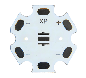
  • High-end and technological sense: Black PCB usually gives people a high-end and technological impression, suitable for high-end electronic products such as high-frequency circuits and high-speed signal transmission circuits, and can provide better signal isolation and electromagnetic interference (EMI) control.
  • High light shielding: Black PCB has high light shielding, and the appearance looks more high-end and atmospheric, suitable for application scenarios that require high aesthetics.
Disadvantages:

  • Complex production process: The production process of black PCB is relatively complex, and it is easy to cause process problems due to insufficient light, such as unclear circuit graphics development, decreased alignment accuracy, etc., which increases the scrap rate and leads to higher costs.
  • Heat absorption: Black PCB absorbs more heat, which may increase the risk of overheating of sensitive components.

Advantages and Disadvantages of Green PCB

Advantages:

  • Widely used and mature process: Green PCB is the most common color, the production process is relatively mature and stable, the curing time is short and the performance is stable, and there are rarely problems such as solder mask bridge shedding.
  • High visibility and contrast: Green PCB contrasts sharply with white text, enhances readability, and is suitable for application scenarios that require high visibility.
  • Environmental protection: The ink used in green PCB is relatively environmentally friendly and does not contain conductive components, which reduces the risk of short circuits and the risk of toxic gas release.

Disadvantages:

  • Traditional appearance: Green PCB gives people a traditional and reliable feeling, which may not be suitable for all high-end or modern design needs.

Application scenario comparison

  • Black PCB: Suitable for high-frequency circuits, high-speed signal transmission circuits, high-end computers and other semiconductor applications because of its good signal isolation and EMI control capabilities.
  • Green PCB: Green PCB is widely used in consumer electronics and industrial control equipment due to its good visibility and recognition.

What is White PCB?

White PCB is a circuit board with a white solder mask on the surface, which is usually used in high-end electronic devices and precision instruments.

1. Definition and characteristics

  • Color: The color of white PCB is limited to white, which makes it more convenient to check the existing circuit.
  • Price: Compared with conventional green PCB, the production cost of white PCB is higher because more processes and special materials are required.
  • Manufacturing difficulty: The manufacturing of white PCB is more complicated than other types of PCB.
Let you know about PCBs of different colors: Black PCB vs green PCB

2. Advantages and disadvantages

Advantages:

  • Beautiful and elegant: The white appearance is more concise and fashionable, suitable for high-end products such as high-end headphones, watches, etc.
  • Easy to identify: During assembly and repair, white PCBs are easier to identify solder joints and components, especially in darker environments.
  • Good thermal conductivity: White PCBs have good thermal conductivity, which helps to dissipate heat and improve product stability and life.

Disadvantages:

  • High production cost: More processes and materials are required during the manufacturing process, resulting in increased costs.
  • Difficult welding test: The surface color is brighter and the light reflectivity is strong, making the welding test process more difficult.
  • Not suitable for high-frequency circuits: Due to the high dielectric constant of white PCBs, they are not suitable for high-frequency circuit design.

What is Yellow PCB?

Yellow PCB refers to a printed circuit board (PCB) with a yellow solder mask (covering layer) coated on the surface. Yellow PCB is not common in PCB manufacturing, mainly because it has a poor contrast with the traces and screen printing, which easily hides the traces and affects readability and visibility.

Characteristics and uses of yellow PCB

  • Poor contrast: Yellow PCB has poor contrast with traces and screen printing, which makes it less visually clear than PCBs of other colors.
Let you know about PCBs of different colors: Black PCB vs green PCB
  • Antistatic layer: Yellow solder resist is often used for antistatic layer, which can effectively prevent static electricity from interfering with the circuit and improve the reliability and stability of the circuit board. In addition, yellow solder resist can maintain its original color after metallization and is often used in radio equipment.

How should the PCB color be selected?

Selecting the right PCB color requires consideration of multiple factors, including the effect of color on readability and aesthetics, the feasibility of the production process, and the needs of the application scenario.

PCBs of different colors and their advantages and disadvantages

  • Green PCB: Green is the most common PCB color and is widely used for its good contrast and readability. The surface treatment of green PCB reflects less light, which helps reduce glare and is suitable for most application scenarios.
  • Red PCB: Red PCB has high visibility and is suitable for high-end electronic devices and parts that need to be highlighted. The red solder resist is easy to control during production, with fewer problems of bubbles and thickness, and is suitable for use in high temperature and harsh environments.
  • Blue PCB: Blue PCB provides good appearance and recognition and is suitable for electronic products that require a high-tech feel. However, the blue solder mask has high fluidity and is prone to oil accumulation, so special attention should be paid during production.
  • Black PCB: Black PCB has high light shielding and aesthetics, but it absorbs heat and increases the risk of component overheating. Black PCB should not be used in high-temperature applications.
  • White PCB: White PCB is easy to identify in low-light environments and is suitable for applications that require high reflectivity, such as lamps and optical equipment.
  • Yellow PCB: Yellow PCB was once widely used, but has poor contrast with routing and screen printing and is now less used.

Recommendations for choosing PCB colors

  • Choose according to application scenarios: If high contrast and readability are required, green or blue PCBs are better choices; if high visibility and high temperature environments are required, red PCBs are more suitable.
  • Consider the production process: Different colors of solder mask have different requirements for the production process, and production efficiency and cost-effectiveness should be considered when choosing.
  • Aesthetics and design style: Choose the right color according to the overall design style of the product, such as red for activeness and enthusiasm, and blue for calmness and technology.

PCBs of different colors each have their own unique advantages and application scenarios. Green PCB is widely used in consumer electronics and industrial control equipment due to its good visibility and recognition. Black PCB is often used in high-performance electronic devices due to its high-end appearance and excellent heat dissipation performance.

As a professional PCB manufacturer, BEST Technology can provide PCBs in a variety of colors to meet the needs of different customers. Whether it is the pursuit of aesthetics or specific functions, we can provide you with high-quality solutions. Please feel free to contact us at sales@bestpcbs.com to get the best PCB color solution.

You may also like

What is the best color for PCB? PCB solder mask colors

January 3rd, 2025

What is the best color for PCB? Generally speaking, green is the best choice for PCB. On the one hand, green solder mask ink is cheap, in sufficient supply, mature in production process, with low scrap rate and obvious cost advantage; on the other hand, it has a sharp contrast with white silk-screen text, which is convenient for seeing circuits and components during assembly and maintenance, and is also environmentally friendly.

What is the standard color of PCB?

In the PCB industry, green is generally regarded as the standard color. This is mainly because:

  • The process is mature and the cost is low: The green solder mask process is the most mature and simple, and the use of green solder mask ink is cost-effective. Most manufacturers use the same green ink, which can reduce the cost of line change and is more economical in large-scale production.
What is the best color for PCB? PCB solder mask colors
  • Good visibility and recognition: The green and white printed text form a sharp contrast, which is convenient for assemblers to scan the circuit board, less stress on the eyes, and good visual contrast when checking welding quality and circuit layout. The visual effect is good in the yellow light room, and the instrument recognition effect for optical positioning and calibration is also better.
  • Relatively safe and environmentally friendly: Compared with other colors such as blue and black, green solder resist does not contain elements such as cobalt and carbon, has a low risk of short circuit when powered on, and generally does not release toxic gases in high temperature environments.

Which PCB color is best?

The choice of PCB color depends on the specific application requirements and environmental conditions. PCBs of different colors have their own characteristics and applicable scenarios:

  • Green PCB: It is the most common color. It is low-cost and has obvious advantages in large-scale production; it is easy to develop and it is easier to remove unnecessary parts during the production process; it has good visual effects and is eye-friendly, which helps the visual contrast of high-brightness metal pads and logos, and is conducive to optical positioning calibration; it also has a certain degree of confidentiality and is relatively safe and environmentally friendly.
  • Black PCB: It gives people a high-end and mysterious feeling and is often used in high-end audio equipment, gaming hardware, etc. The contrast of the words marking the welding parts is high, and the colored connectors are more conspicuous against a black background, and the visual effect is good when placed in the chassis. However, the production process of black PCB has high process requirements, which is easy to cause color difference, resulting in an increase in defective rate, and the circuit routing is difficult to identify, which will increase the difficulty of maintenance and debugging in the R&D and after-sales stages.
  • Blue PCB: It can provide novel and high-end visual effects, suitable for electronic products that pursue product appearance differentiation, with good screen printing contrast, relatively simple production process and moderate cost.
What is the best color for PCB? PCB solder mask colors
  • Red PCB: It has excellent visibility, can clearly define the contrast of traces, planes and blank areas, and has beautiful screen printing effects. It usually uses high-temperature resistant red photosensitive dyes, has good thermal stability and weather resistance, and is often used in specific applications such as high-end communication equipment and military electronics, but the production process is complex and the cost is high.
  • White PCB: The appearance is clean and beautiful, suitable for products with high decorativeness, such as high-end headphones, watches, etc. However, it is easy to hide the routing, the production cost is relatively high, and the welding test is relatively difficult.

Does PCB color matter?

PCB color is important to a certain extent.

From the perspective of manufacturing, color is related to production process. The production process of green PCB is the most mature and the cost is relatively low. Because green solder mask ink is more commonly used, manufacturers can use equipment and materials more efficiently and reduce production costs during large-scale production.

Black PCBs have higher process requirements during the manufacturing process. For example, in the exposure and development stages, black solder mask may require more precise parameter control due to its strong light shielding, otherwise it is easy to have quality problems, such as short circuit hazards or appearance defects.

Color also has an impact on the product assembly and maintenance stage. For assembly workers, the high contrast between green PCB and white silk-screen text makes it easier for them to identify component locations and view line directions, which helps improve assembly efficiency and reduce the probability of errors. Black PCBs have disadvantages in this regard. Its lines are not easy to see clearly, which is more troublesome during debugging and maintenance.

From the perspective of product performance, color may have a certain impact on heat dissipation and electromagnetic compatibility (EMC). In theory, black PCBs may have better performance in thermal radiation due to their darker color, which can help some high-power devices dissipate heat better.

In terms of electromagnetic shielding, if special additives are used to change the color of PCBs of different colors, these materials may affect the electromagnetic shielding performance. However, this situation is more complicated and related to the specific material formula.

In terms of product appearance design, color is very important. For consumer electronic products, such as mobile phones and computers, the color of the PCB can match the overall style and brand image of the product. For example, some high-end electronic products use black PCBs to create a cool and professional feeling, while some products with a fresh style may use white or light blue PCBs.

Are black PCBs more expensive?

Usually, black PCBs are more expensive for the following reasons:

  • Material cost: Black solder mask materials may require more expensive pigments or additives, and character inks may also be more expensive due to color and quality factors.
  • Production process: Black pigments absorb light strongly. In the exposure and development processes, it is easy to have process problems such as unclear circuit graphics due to insufficient light and reduced alignment accuracy between the solder mask and the circuit, which increases the scrap rate and leads to an increase in overall costs.
  • Market demand and supply: Black PCB is generally used in high-end electronic products, and the market demand is relatively small. Suppliers cannot form economies of scale during production, which leads to an increase in unit price.

Why is green PCB cheaper?

Green PCB is cheaper for the following reasons:

1. Low material cost:

  • Cheap raw materials: The raw materials of green solder mask ink are in sufficient supply in the market and are relatively cheap. For example, compared with the expensive pigments or additives used in some special color inks, the cost of green ink ingredients is lower.
  • Adequate stock: Due to the widespread use of green PCBs, ink suppliers usually reserve a large amount of green ink, which further reduces procurement costs and reduces the risk of price fluctuations caused by shortages.
What is the best color for PCB? PCB solder mask colors

2. Mature production technology:

  • Easy to process: The processing and printing of green solder mask ink is relatively easy, and no complex color adjustment and special treatment are required during the production process, which can improve production efficiency and reduce labor and time costs.
  • Low scrap rate: The process of producing green PCB is very mature. In the exposure, development and other processes, the probability of quality problems of green PCB is low, and the scrap rate is low, which reduces the overall production cost.

3. Favorable market supply and demand relationship:

  • Massive production: Green is the most common color of PCB, and the market demand is large, so manufacturers can carry out large-scale production. Through large-scale production, enterprises can make full use of production equipment and reduce the production cost of unit products.
  • Strong versatility: Most electronic products have no special requirements for PCB color. Green PCB can meet the needs of most application scenarios. There is no need to adjust the production line or increase additional costs to meet the special color requirements of individual customers.

What color is FR4?

FR4 is a substrate material for PCB. It does not have a fixed color. Its main components are glass fiber cloth and epoxy resin. Its color is usually determined by the solder mask on the surface.

The most common color of FR4 circuit boards is green, because green solder mask is widely used in PCB manufacturing. But in fact, FR4 substrate can present a variety of colors after different surface treatments, such as black, blue, red, white, etc.

How to choose the color of PCB?

There are several main factors to consider when choosing the color of PCB:

1. Functional requirements:

  • Green PCB: Green PCB is widely used because of its high clarity and low glare characteristics. The green solder mask contrasts sharply with the white text, improving readability while reducing glare and protecting the eyes.
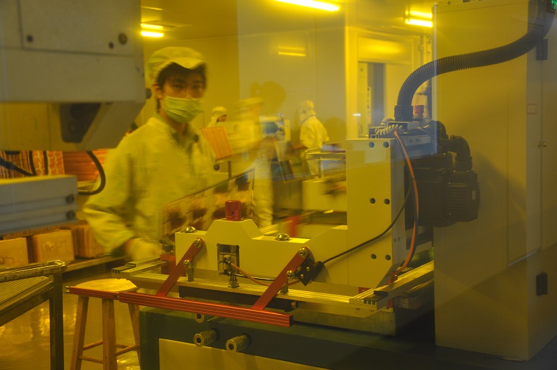

  • Black PCB: Black PCB provides high light shielding and aesthetics, and looks high-end and atmospheric, but it absorbs more heat and may increase the risk of overheating of sensitive components.
  • Blue PCB: Blue PCB has good screen printing contrast and is suitable for applications that require high contrast, such as LCD installation.
What is the best color for PCB? PCB solder mask colors
  • Red PCB: Red PCB is eye-catching and has high visibility, suitable for high-end electronic devices and occasions that require high-precision circuit boards.

  • White PCB: White PCB appears clean and tidy in various environments, has high reflectivity, and is suitable for low-light environments or applications that require high contrast.
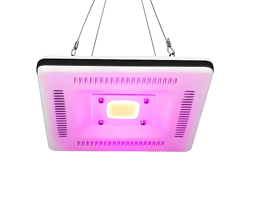
2. Application scenarios and environmental factors:

  • Consumer electronics: Green PCB is widely used in consumer electronics due to its low cost and high contrast.
  • High-end electronic equipment: Red and blue PCB are often used in high-end communication equipment, military electronic products and optical equipment due to their high visibility and contrast.
  • Lighting industry: White PCB is often used in the lighting industry due to its high reflectivity.

3. Production process and cost-effectiveness:

  • Production process: PCBs of different colors have different requirements for production process.
  • Cost-effectiveness: Green PCB is the most widely used, and factories usually reserve a large amount of green paint, which is relatively low in cost. In addition, green is more friendly to the eyes and reduces fatigue caused by long-term work.

In short, the selection of PCB color should be considered comprehensively. If you pursue cost-effectiveness and mass production, choose green, which has low cost and mature technology; if you want to highlight the quality of high-end products, you can choose black, which has high cost but good appearance and texture; blue, red, etc. are determined according to specific scenarios, such as red for high visibility and blue for novel appearance. Comprehensive consideration can be made to choose the right one.

You may also like