Exciting news for all PCB designers, engineers and related industries!
EBest Circuit (Best Technology), one of Chinaâs most trusted PCB manufacturing and assembly partners, is thrilled to announce our participation at Southern Manufacturing & Electronics 2026, taking place in the UK from February 2ndâ5th (Western Time). Youâll find us at Booth No. K60 â ready to connect, collaborate, and inspire.
If you missed meeting us at New Tech or PCB West, this is your perfect opportunity to catch up with our team in person!
What Youâll See at Booth K60
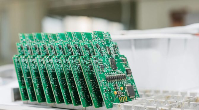
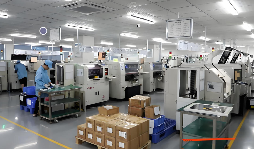
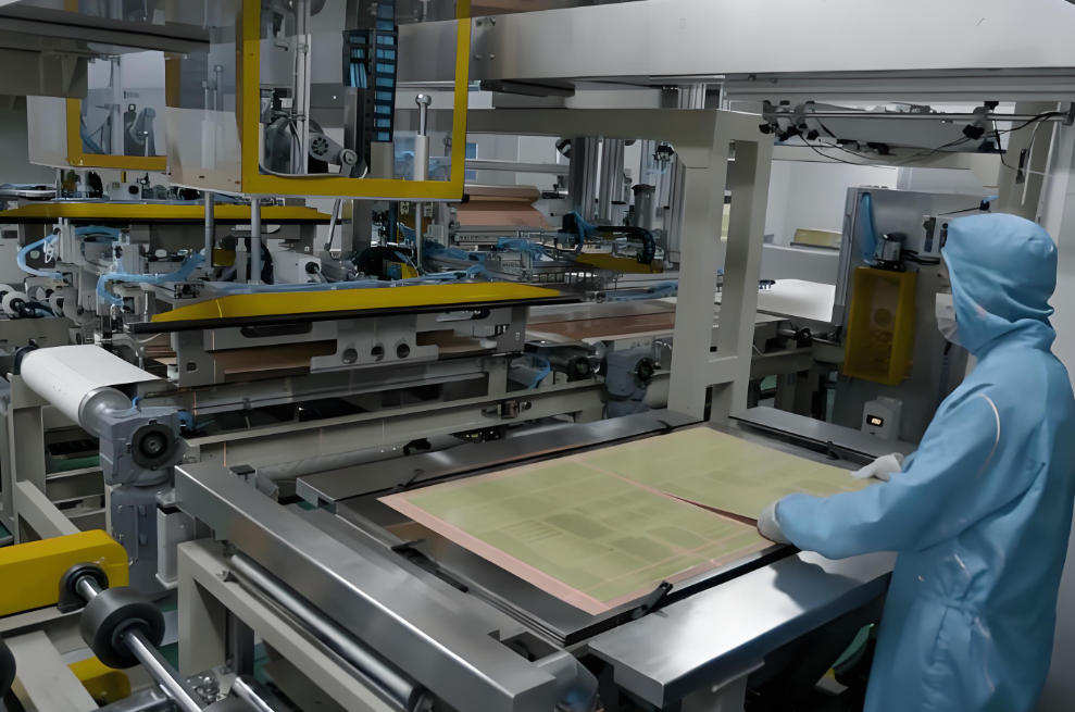
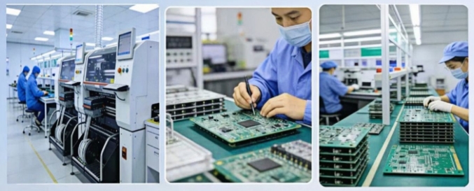
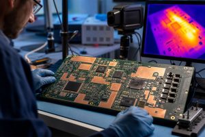
At the show, youâll get hands-on insights into our advanced PCB manufacturing and assembly technologies. Our engineers will be available to discuss every step of the process â from PCB rapid prototyping to low and high-volume production â and demonstrate how we achieve precision, reliability, and speed in every board we produce.
Visitors can explore a full spectrum of PCB solutions, including:
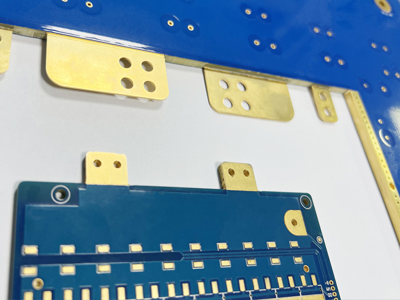
Comprehensive services, from component sourcing and board fabrication (FPC, PCB, MCPCB, Ceramic PCB) to final assembly, programming, and testing
Our full turnkey service covers everything from component sourcing, PCB fabrication, SMT assembly, testing, programming, to final system integrationâall handled under one roof for seamless project execution.
What Youâll Learn
During the exhibition, our engineering team will be available to discuss:
How we minimize component wastage through process optimization
Strategies to reduce production costs and shorten lead times
The latest trends in PCB technology
Best practices for reliable high-density interconnect (HDI) designs
Whether you are in the early stages of product design or managing mass production, our experts will share actionable insights to help streamline your next project.
Event Details
Show Opening Times:
Tuesday, February 3: 09:30 â 16:30
Wednesday, February 4: 09:30 â 16:30
Thursday, February 5: 09:30 â 15:30
Address: Farnborough International Exhibition Centre, UK â Hall 1
If you want to know more about this showcase, click below:
Full Certifications: ISO9001 | ISO13485 | IATF16949 | AS9100D | UL | RoHS
FREE Stack-Up Suggestions
Free DFM, DFA and DFT check
100% original components from authorized distributer
100% Testing – Flying probe, function testing, ICT, etc
Quality control system – X-ray, AOI, FAI
IPC class II, IPC class III, IPC 3/A standard
Join Us in the UK
If you missed meeting us at New Tech or PCB West, this is your next chance to connect in person. Stop by our booth to see how weâre advancing PCB performance through innovation, precision, and dedication to quality.
We look forward to meeting you in Farnborough, UK, and discussing how EBest Circuit (Best Technology) can support your next electronics project.
How to assemble HDI PCB? Let’s discover benefits, applications, manufacturing process, manufacturer recommendations for HDI PCB assembly.
Are you worried about these problems?
Struggling with high-density routing complexity and time-consuming design revisions?
Facing yield instability and cost control issues under miniaturization demands?
Tight deadlines and urgent orders causing production scheduling headaches?
As a HDI PCB assembly manufacturer, EBest Circuit (Best Technology) can provide you solutions:
Dedicated HDI design team with DFM-driven early engagement to slash trial cycles by 30%+;
Smart layer stacking optimization + laser microvia tech ensuring micro-spacing reliability, stabilizing yield at 98%+ while cutting costs by 15%;
Agile capacity pool + real-time scheduling system for 7-day rush order response and 24/7 lead time tracking.
Welcome to contact us if you have any issues with HDI PCB assembly: sales@bestpcbs.com.
What Is HDI PCB Assembly?
HDI PCB Assemblyrefers to the process of soldering and interconnecting electronic components on highly compact and complex High Density Interconnect circuit boards using advanced manufacturing techniques, such boards include the use of microvias (e.g., blind or buried vias formed via laser drilling), finer line widths/spacings, increased routing layers, and tightly stacked interlayer technologies, enabling significantly higher routing density and electrical connection complexity within smaller areas compared to traditional PCBs.
This assembly process demands ultra-high-precision placement equipment (such as for miniature BGA or CSP chips), precise soldering techniques (e.g., laser soldering or specialized reflow processes), and rigorous inspection methods to ensure reliable electrical connections and functionality of all components and microvia interconnections in such miniaturized spaces.
Maximizing Space Utilization Efficiency: HDI technology employs microvias, blind vias, and buried vias to drastically reduce wiring area, enabling complex circuit layouts within limited space. This supports compact structural designs for volume-sensitive products like smartphones and wearables.
Enhancing Electrical Performance and Signal Integrity: Shortened signal transmission paths minimize impedance and signal attenuation while reducing electromagnetic interference (EMI). This ensures stable data transmission quality in high-frequency applications such as 5G communication devices.
Increasing Design Flexibility and Integration: Supports high-density arrangement of components on double-layer or multi-layer boards, allowing seamless integration of complex functional modules (e.g., processors, sensors). Any-Layer Interconnect (ELIC) schemes break traditional PCB wiring constraints.
Improving Reliability and Durability: Microvia technology reduces mechanical stress concentration points, enhances thermal cycling performance, and extends product lifespan. Stringent lamination and copper plating standards lower connection failure risks, meeting high-reliability demands in automotive electronics and medical devices.
Accelerating Product Development Cycles: HDI design facilitates rapid prototype verification, streamlines debugging processes, and shortens the transition from design to mass production. Strong compatibility with simulation tools optimizes pre-development schemes and reduces trial-and-error costs.
Reducing Long-Term Comprehensive Costs: Although initial costs are higher, HDI reduces material layers, optimizes assembly processes, and lowers material and labor inputs. Higher yield rates and product reliability minimize post-sales maintenance expenses, boosting overall economic efficiency.
Driving Technological Iteration and Innovation: Serves as a carrier for advanced packaging technologies (e.g., wafer-level packaging), supporting R&D in cutting-edge fields like AI chips and IoT devices. Compatible with new materials (e.g., high-frequency substrates) to adapt to future electronic technology evolution.
Environmental and Sustainability Benefits: Precise material usage minimizes waste and complies with environmental standards like RoHS. Energy-efficient designs reduce power consumption in end products, aligning with green manufacturing trends.
Portable medical devices (ultrasound diagnostic instruments, blood glucose monitors)
Implantable medical devices (pacemakers, nerve stimulators)
Satellite communication modules
Military radar and navigation systems
Server and data center motherboards
Edge computing devices
Industrial PLCs
Smart home controllers
HDI PCB Assembly Manufacturing Processes
1. Incoming Quality Control (IQC)
Visual Inspection: Use high-magnification microscopes or automated optical inspection systems to detect defects on HDI PCB bare boards (e.g., scratches, copper peeling, solder mask delamination) and electronic components (e.g., oxidized/bent leads).
Soldability Testing: Conduct wetting balance tests to evaluate solder paste adhesion to pads/component leads; perform thermal shock tests for surface finishes like OSP/ENIG.
Standards Compliance: Cross-reference IPC-A-610 for pad design/solder mask tolerances; JEDEC standards for chip package dimensions; ASTM D2794 for adhesion testing.
Batch Traceability: Implement barcode/QR code systems to track material batches, suppliers, and storage dates for full lifecycle traceability.
2. Solder Paste Printing
Stencil Design: For fine-pitch components (e.g., 01005), use electroformed nickel stencils with ±5Όm aperture accuracy; implement stepped stencils for BGA/CSP areas to control solder volume.
Machine Parameters: Set squeegee pressure (2-5N/cm?), print speed (50-150mm/s), and snap-off speed (0.1-0.3mm/s); employ SPI (Solder Paste Inspection) for real-time 3D measurement of print thickness (0.08-0.15mm) and alignment (±15Όm).
Quality Control: Utilize 3D SPI for defect detection (bridging, insufficient solder, misalignment); perform localized magnified inspection for microvia regions; document parameters in a process database.
3. Surface Mount Technology (SMT) Placement
Equipment Precision: High-precision pick-and-place machines achieve ±15ÎŒm accuracy for 01005 (0.4mmĂ0.2mm) components; vision systems enable precise BGA/CSP alignment.
Process Optimization: Conduct DOE (Design of Experiments) to determine optimal placement pressure/nozzle height; implement segmented placement strategies (large components first, then small ones).
Special Handling: Use vacuum nozzles/non-contact grippers for QFN/LGA devices; configure dedicated placement heads for temperature-sensitive components with controlled speed.
4. Reflow Soldering
Temperature Profile Control: Utilize 10-zone reflow ovens with zones for preheat (150-180°C), soak (180-200°C), peak (217-227°C for lead-free alloys), and cooling (3-5°C/s); monitor via thermocouples.
Material-Specific Adjustments: Raise peak temperatures to 245-255°C for SAC305 solder; implement nitrogen inerting for high-speed/high-frequency substrates (e.g., Rogers 4350B).
Defect Prevention: Perform thermal simulation to predict stress distribution; conduct board-level reliability testing (-55°C~125°C thermal cycling) for BGA packages; monitor oven uniformity via infrared thermography.
5. Automated Optical Inspection (AOI)
Detection Algorithms: Deploy deep learning for 01005 component defects (misalignment, tombstoning); multi-angle lighting for bridging/insufficient solder detection; tilted-view imaging for QFN bottom terminations.
Data Traceability: Generate inspection reports with images/defect locations; integrate with MES for real-time production data synchronization.
6. Through-Hole Technology (THT) Insertion
Insertion Strategy: Use selective insertion machines for high-density areas; equip manual stations with ESD workbenches/magnifiers.
Process Control: Monitor insertion depth via force sensors; pre-form THT leads (e.g., 90° bending) to suit HDI density constraints.
Soldering Protection: Shield SMD areas with fixtures; apply localized cooling for temperature-sensitive components; optimize wave solder parameters (time/temperature) to minimize thermal impact.
7. Wave & Selective Soldering
Wave Parameters: Set wave temperature (250-260°C), height (8-12mm), and conveyor speed (1.0-1.5m/min); employ nitrogen inerting to reduce oxidation.
Selective Soldering: Use robotic solder nozzles for point-to-point welding; laser alignment ensures precision; dual-nozzle systems for high-power device leads.
Defect Detection: Perform X-ray inspection for hidden joints; conduct pull testing for mechanical strength; use dye penetrant tests for micro-cracks.
8. Hand Soldering & Rework
Tool Configuration: Equip 200-300W soldering stations with microscopes/vacuum desoldering tools; use lead-free solder (Sn96.5Ag3Cu0.5) with temperature control.
Operational Standards: Standardize rework procedures (heat first, then add solder); employ BGA rework stations for precision temperature control; apply localized cooling for sensitive parts.
Quality Validation: Microscopic inspection for wetting quality; electrical testing for functional recovery; document rework processes for traceability.
9. Cleaning & Coating
Cleaning Process: Ultrasonic cleaning with aqueous detergents for flux removal; solvent cleaning (e.g., n-hexane) for high-reliability applications with exhaust treatment.
Coating Techniques: Automated conformal coating with acrylic/silicone/polyurethane; measure film thickness (25-75ÎŒm) via thickness gauges; localized reinforcement for critical areas.
Potting Process: Encapsulate with two-part epoxy resins; vacuum degassing for bubble removal; thermal curing with insulation resistance testing.
10. Testing & Burn-In
Electrical Testing: ICT uses bed-of-nails fixtures for component-level testing; flying probe testers contact high-density points without dedicated fixtures; boundary scan (JTAG) for chip-level tests.
Functional Verification: FCT simulates operational conditions (power fluctuations, signal interference) for system validation; eye diagram tests for high-speed digital circuits; S-parameter measurements for RF circuits.
Reliability Testing: Conduct 85°C/85%RH tests, -55°C~125°C thermal cycling, and vibration testing (sine/random); perform shear testing for critical solder joints.
11. Packaging & Logistics
Packaging Standards: Multi-layer packaging with ESD shielding bags, foam, and desiccants; vacuum packaging for precision components; reinforced crates for large PCBAs.
Logistics Tracking: Implement barcode/RFID systems for product traceability; monitor temperature/humidity during transit; secure high-value shipments with insurance.
Documentation: Provide complete process files (BOMs, parameter sheets), test reports, and reliability data; integrate with EDMS (Electronic Document Management System).
19 Years of Dedicated HDI Expertise: With 19 years of focused experience in HDI PCB assembly, we cover full-spectrum HDI technologies from 2-stage to 8-stage any-layer solutions. Having completed over 5,000 high-complexity projects, we deliver proven process expertise and problem-solving capabilities as your reliable long-term technical partner.
ISO-Certified Quality Control System: Adhering to IPC-A-610E/620A standards and our proprietary “dual-inspection, triple-review” process, we implement 360° full-chain traceability from component incoming to final shipment. Defect rates are controlled below 50PPM, with products certified to ISO9001/14001 and RoHS standards, ensuring zero-defect precision for every board.
Competitive Price: Through scaled production, lean supply chain management, and process optimization, we offer prices 15%-20% below market averages while maintaining cost advantages for premium materials (e.g., high-frequency substrates) and specialized processes (e.g., blind/buried vias, microvia filling), maximizing your cost-performance value.
One-Stop Solutions: From PCB design optimization and BOM sourcing to SMT assembly, testing, and logistics, we provide end-to-end integrated services that reduce supplier coordination efforts, shorten project timelines by over 30%, and deliver true turnkey convenience.
Fast Delivery for Market Leadership: Leveraging intelligent production scheduling and flexible capacity allocation, standard HDI projects achieve 7-day prototyping and 15-day volume production. Urgent orders are supported with 48-hour expedited responses, enabling faster market entry and competitive advantage.
Precision Equipment for Micron-Level Accuracy: Equipped with imported systems like JUKI high-speed placement machines, combined with AOI and X-ray inspection, we achieve ±0.05mm microvia processing accuracy and 01005 component placement capability to meet the most demanding design specifications.
Custom R&D Support for Technical Challenges: Our 30+ senior engineers provide full-chain technical support, including DFM analysis, signal integrity simulation, and development of specialized processes (e.g., rigid-flex boards, embedded components), helping you overcome technical barriers and drive innovation.
Sustainable Manufacturing for Global Compliance: We employ lead-free processes, water-based cleaning agents, and recyclable packaging while complying with EU REACH, halogen-free, and other environmental regulations. Carbon footprint tracking optimizes energy use, ensuring seamless compliance with global green standards.
Our Quality Inspection for HDI PCB Assembly
Raw Material Inspection
Substrate Testing: Utilize TMA thermomechanical analyzer and dielectric constant tester to validate dielectric constant (Dk deviation †±0.05, frequency range 1MHz-10GHz), CTE (Coefficient of Thermal Expansion â€12ppm/â, -50â to 250â), and water absorption rate (â€0.1%).
Copper Foil Inspection: Employ universal material testing machine to ensure thickness deviation †±5% (precision 0.1ÎŒm), tensile strength â„250MPa (electrodeposited copper) / â„300MPa (rolled copper), and peel strength â„0.7kgf/cm.
Laser Drilling Inspection: Use X-ray fluorescence thickness gauge and optical microscope to verify hole diameter tolerance †±3% (hole size â€0.15mm), copper wall thickness deviation â€1ÎŒm, and ensure hole position tangent to target pad without pad damage.

Plating Layer Inspection: Validate copper/nickel/gold layer thickness compliance with design specifications (precision 0.01ÎŒm) and fixed plating current density at 1.5A/dmÂČ (verified via DOE) using film thickness tester.
Laminate Quality Inspection: Employ metallographic microscope and thermal stress tester to confirm layered dielectric thickness â„40ÎŒm after lamination (minimum thickness â„30ÎŒm) and absence of bubbles/delamination.
Inline Detection
AOI Optical Inspection: Deploy high-precision AOI equipment to detect line width deviation †±10% (pixel accuracy 0.001mm), identify defects like shorts/opens/metal residues, maintain false call rate â€0.1%, and achieve detection speed â„1m/min.
X-ray Inspection: Utilize X-ray detection system to check blind/buried via alignment accuracy â€0.005mm, detect copper voids/layer misalignment, and enable full-board non-destructive testing.
Solder Joint Reliability Testing: Perform thermal shock (-55â to 125â, 1000 cycles, solder joint failure probability â€1%) and dynamic bending (flexible PCB, bending radius 5mm, 10000 cycles no fracture) using thermal shock chambers and bending testers.
Signal Integrity Testing: Measure signal loss, delay, and noise using high-speed oscilloscopes and network analyzers to ensure transmission stability meets design requirements.
Our HDI PCB Assembly Capabilities
Item
Capabilities
Placer Speed
13,200,000 chips/day
Bare Board Size
0.2 x 0.2 inches – 20 x 20 inches/ 22*47.5 inches
Minimum SMD Component
01005
Minimum BGA Pitch
0.25mm
Maximum Components
50*150mm
Assembly Type
SMT, THT, Mixed assembly
Component Package
Reels, Cut Tape, Tube, Tray, Loose Parts
Lead Time
1 – 5 days
How to Get a Quote For HDI PCB Assembly Service?
All Documents for HDI PCB Assembly Service Quotation:
Bill of Materials (BOM): Detailed list of components with model numbers, specifications, quantities, and supplier information for material procurement and cost calculation.
Drill Files: Clear specifications of hole positions, diameters, and types (e.g., blind/buried vias) to meet HDI high-density routing requirements.
Assembly Drawing/Coordinate Files: Precise coordinates of components on the PCB to guide SMT placement and soldering, avoiding misalignment.
Process Parameters: Surface finish (e.g., ENIG, HASL), solder mask color, substrate material (FR4/high-frequency), board thickness, layer count, and special processes (e.g., blind/buried vias, microvia filling).
Test Verification Files: Test point diagrams and functional test plans to validate circuit performance.
Quantity & Lead Time Requirements: Production batch size (prototype/small batch/mass production), delivery time, and urgency level affecting production scheduling and costs.
Contact & Contract Information: Company name, contact person, contact details, and agreement clauses for communication and legal compliance.
Welcome to contact us if you have any request for HDI PCB assembly: sales@bestpcbs.com.
How to design a keyboard PCB? Let’s explore material selection, design software, design guide, technical parameter for keyboard PCB design.
Are you troubled with these problems?
How to overcome the dual challenges of key signal crosstalk and electromagnetic interference under high-density layout?
How to achieve cost-effective small-batch prototyping while maintaining flexible scalability for large-order rapid turnover?
How to ensure full-cycle timeliness from design verification to mass production delivery, avoiding project delay risks?
As a keyboard PCB manufacturer, EBest Circuit (Best Technology) can provide you service and solutions:
Electromagnetic Compatibility Optimization Plan: Adopt optimized differential signal routing + intelligent ground plane segmentation technology to achieve 30% improvement in signal integrity and reduce crosstalk to industry-leading levels.
Flexible Capacity Management Platform: Modular production architecture supports 10-piece prototyping without price surcharge and enables 48-hour rapid response for 10,000-piece rush orders, boosting inventory turnover by 50%.
Rapid Delivery Guarantee System: Full-process standardized management from DFM manufacturability verification to final product testing ensures 48-hour delivery for standard orders and compresses complex project cycles to 70% of industry average duration.
Prioritize FR4 epoxy fiberglass substrate for most consumer-grade keyboards, balancing cost and electrical stability. For high-strength scenarios, upgrade to 2.0mm thickness or use aluminum substrates to enhance heat dissipation and structural rigidity.
Flexible keyboard designs require polyimide (PI) substrates, with validation of bend resistance cycles and lamination process compatibility.
For high-frequency RGB lighting or switches, use high-frequency specialized substrates (e.g., PTFE, ceramic-filled) with Df <0.005 to minimize signal loss.
Thermal Management Requirements
Standard scenarios require high-Tg FR4 (Tg â„130°C) to prevent solder joint thermal failure. High-heat scenarios (e.g., RGB-backlit keyboards) utilize aluminum substrates (thermal conductivity â„1.0 W/m·K) or copper substrates for enhanced heat dissipation.
Coefficient of thermal expansion (CTE) must match copper foil to prevent pad detachment under temperature changes, with recommended CTE â€15ppm/°C.
Environmental Compliance & Regulations
EU markets require compliance with RoHS 3.0 and REACH regulations, prohibiting hazardous substances like lead and halogens. Asian markets prioritize UL-certified eco-friendly substrates.
Industrial/outdoor keyboards need salt spray test certification, using moisture- and corrosion-resistant enhanced FR4 (glass fiber content â„30%).
Special Process Compatibility
High-density designs (e.g., blind/buried vias, back-drilling) require substrates compatible with HDI processes. Ultra-thin keyboards use 1.0mm ultra-thin FR4 or flexible PI substrates to ensure manufacturing yield.
Modular designs adopt recyclable bio-based epoxy resins to extend product lifecycle and reduce electronic waste.
Common Software for Keyboard PCB Design
Altium Designer: A comprehensive professional-grade tool supporting end-to-end design from schematic to layout and routing, ideal for complex projects.
KiCad: An open-source, free software offering schematic design, PCB layout, and 3D visualization, suitable for small-to-medium projects and individual developers.
Autodesk Eagle: Geared toward small-to-medium designs, featuring a clean interface and free tier, commonly used for entry-level and rapid prototyping.
Cadence OrCAD: A professional-grade solution enabling advanced simulation and collaboration features, designed for industrial-grade complex circuit design.
PADS PCB Design: Focused on streamlining the design process, providing efficient layout and debugging tools for small-to-medium circuit board projects.
EasyEDA: A cloud-based, free tool integrating shared libraries and collaboration capabilities, perfect for quick design and project sharing.
Fritzing: Targeted at makers and hobbyists, offering simplified PCB design capabilities for educational and small-scale projects.
Keyboard Type and Layout: Refine mechanical keyboard switch selection (e.g., Cherry MX, Gateron), optimize membrane keyboard tactile feel, and customize keycap compatibility for personalized keyboards. Layout specifications include full-size (104 keys), 60% (68 keys), split (e.g., Ergodox) key spacing and ergonomic tilt angles (e.g., 5°-12° keycap inclination), with support for hot-swappable socket types (e.g., 3pin/5pin MX-compatible).
User Scenario Adaptation: Office scenarios prioritize low-noise switches (e.g., silent red switches) and anti-misoperation Fn key combinations. Gaming scenarios require 0.1ms response speed, programmable macro keys, and dynamic RGB lighting (e.g., wave mode, breathing light). Portable scenarios focus on lightweight design (e.g., acrylic case), Bluetooth/wired dual-mode connectivity, and battery life (e.g., 5000mAh lithium battery supporting 300 hours of standby).
International Standards and Ergonomics: Adhere to ANSI/ISO dual-standard key mapping and support multilingual switching (e.g., Chinese/English, Japanese kana input). Ergonomic optimizations include keycap curvature (e.g., spherical keycaps), wrist rest silicone pads, and adjustable tilt brackets (e.g., three-stage foot supports).
2. Plan Circuit Architecture and Matrix Design
Matrix Design Balance: Utilize dynamic scanning algorithms to optimize row/column ratios (e.g., 8×16 matrix), eliminate “ghosting” via reverse-parallel diodes, and support NKRO (n-key rollover) mode.
Main Controller Selection: Choose ARM Cortex-M4/M7 series (e.g., STM32F411) or dedicated keyboard MCUs (e.g., ATmega32U4), integrating USB HID protocol stacks, multi-key parallel recognition logic, and macro command storage (e.g., 128KB Flash supporting 500 macro instructions).
Power Management Module: Implement 3.3V regulation via LDOs (e.g., TPS73733), integrate over-voltage protection (OVP), over-current protection (OCP), and ESD protection (e.g., TVS diode arrays), with low-power modes achieving standby current below 1ÎŒA (achieved via sleep mode + wake-up interrupts).
Pad and Keycap Fixing: Hot-swappable pads compatible with MX switches (19.05mm pitch), keycap fixation supporting PCB mount (screw-fixed) or onboard snap-fit designs, with ENIG (electroless nickel gold) surface treatment for improved solderability.
High-Speed Signal Processing: USB data lines use equal-length routing (±5mil error), differential pairs maintain 3x line width spacing, add common-mode chokes to suppress EMI, and place ESD protection devices near interface terminals (e.g., USBLC6-2SC6).
Integrated Extension Functions: I2C interface connects OLED displays (128×32 resolution), SPI interface drives RGB light strips (WS2812B), programmable knobs read analog signals via ADC for volume/brightness adjustment, and reserved PMOD interfaces support sensor expansion (e.g., accelerometers).
Debugging and Firmware Update: Integrated SWD interface (2.54mm pitch) supports ISP programming, test points (matrix nodes, power pins) facilitate multimeter/logic analyzer debugging, and firmware updates are achieved via DFU mode for wireless upgrades (e.g., Bluetooth OTA).
5. Maintainability and Compatibility Design
Modular Structure: Main control board and sub-board separated via 24-pin FPC connectors, supporting hot-swappable upgrades (e.g., controller chip upgrades), positioning plates compatible with steel/acrylic/PC materials, and standardized assembly via M2 screw holes.
Cross-Platform Compatibility: Firmware compatible with QMK/ZMK open-source frameworks, supports multilingual key mapping (e.g., layout switching via key combinations), cross-OS compatibility with Windows/macOS/Linux and Android/iOS devices, plug-and-play without driver installation.
Expandability Design: Reserved expansion interfaces (e.g., GPIO pins) support future upgrades (e.g., adding touchpads), case design supports magnetic keycap replacement and custom sticker areas.
Prototype Testing: Verify full-key no-ghosting via matrix scanning algorithms, test USB communication stability via 100,000 plug-in cycles, and measure power consumption for dynamic current monitoring (e.g., standby current below 100ÎŒA, operating current below 50mA).
Compatibility Testing: Cover Windows 7/10/11, macOS 12+/Linux (Ubuntu/Debian), and Android 11+/iOS 15+ devices, validate HID protocol compatibility and multi-device switching response times (below 500ms).
7. Documentation and Design for Manufacturability (DFM)
Production Documentation: Generate BOM lists (including component models, suppliers, inventory info), Gerber files with layer stackup, solder mask openings, drilling files, coordinate files for SMT machine assembly, and specify PCB parameters (e.g., 1oz/2oz copper thickness, HASL/ENIG surface finish, solder mask color like black matte).
DFM Optimization: Tolerance for pad dimensions ±0.1mm, minimum trace width/spacing 4mil/4mil, via types use buried+blind via combinations to reduce interlayer crosstalk, panelization employs V-cut scoring + stamping holes for improved production efficiency.
Version Control: Use Git for design change tracking, version numbers follow semantic versioning (e.g., v1.0.0), design documentation includes change logs, test reports, and multilingual user manuals.
Keyboard PCB Design Technical Parameter
Technical Parameter
Typical Value / Range
PCB Thickness
1.2mm, 1.6mm
Form Factor & Layout
ANSI, ISO, TKL, 60% etc.
Mounting Holes
Compatible with GH60 and other standards
Layer Count
2-layer, 4-layer
Copper Thickness
1 oz (35ÎŒm)
Min Trace/Space
0.15mm (6 mil)
Power Trace Width
0.4mm – 0.8mm
Switch Type
Mechanical, Hot-swappable, Magnetic
Matrix Scan Rate
1kHz – 10kHz
Debounce Time
5ms – 25ms
Main Controller Interface
USB Type-C
Connectivity
Wired, Tri-Mode (2.4G/Bluetooth/Wired)
Report Rate
1kHz, 8kHz
RGB Lighting
Supports WS2812B etc.
Firmware Support
QMK, VIA, VIAL
ESD Protection
Integrated TVS Diodes
Surface Finish
ENIG, HASL, Immersion Gold
Solder Mask Color
Multiple options (Green, Black, White etc.)
Min Via Diameter
0.3mm
Keyboard PCB Layout & Routing Techniques
Efficient Key Matrix Layout
Partition Optimization: Adopt “checkerboard” or “staggered” partition designs, grouping keys by functional modules (e.g., letter zone, number zone, function key zone, edit zone) to reduce cross-region routing length and signal crosstalk risk. For 60% layout keyboards, balance key spacing (typically 18-19mm) and routing density in compact spaces, avoiding signal cross-talk in high-frequency areas like WASD gaming zones. 65%/75% layouts can add dedicated arrow key or F-row partitions for enhanced usability.
Row/Column Routing Strategy: Implement orthogonal layouts for row and column lines to avoid long parallel traces; critical row/column lines can be widened to 0.2-0.25mm to reduce signal delay and improve matrix scanning stability. For full-size (100%) keyboards, “serpentine” routing can minimize cross-layer vias and signal reflection risks.
Grounding Strategy: Deploy dense grounding vias (spacing â€5mm) near MCUs and LED backlight modules to form “ground islands” reducing EMI. ESD protection devices (e.g., TVS diodes) must be placed close to interfaces, with ground terminals directly connected to the ground plane to ensure the shortest electrostatic discharge path. For multi-layer boards, “ground via arrays” can enhance inter-layer connectivity and reduce ground impedance.
USB Differential Pair Optimization: USB Type-C differential pairs (D+/D-) must maintain equal length (error â€5mil), equal spacing (10-15mil), and trace length â€200mm without cross-layer vias. Top-layer differential pairs can be wrapped with ground shielding traces (spacing 0.1-0.2mm), while inner-layer pairs should neighbor ground planes to reduce EMI radiation. For USB 3.0/3.1, “impedance-controlled” routing with ±10% tolerance and common-mode chokes are required to suppress EMI.
Impedance Control: Critical signal lines (e.g., clock, data) should be designed with impedance calculation tools (e.g., Saturn PCB) within ±10% tolerance. Sensitive signals (e.g., backlight data) should avoid proximity to high-frequency noise sources (e.g., switching power supplies, crystals) and use “shielding layers” for enhanced noise immunity.
Manufacturability and Testability
Minimum Trace Width/Spacing: Strictly adhere to 0.15mm (6mil) minimum trace width/spacing specifications to avoid manufacturing defects. Via sizes should be â„0.3mm (minimum hole size) with “thermal relief” designs for better adhesion. For high-density routing, “blind/buried vias” can reduce inter-layer connection lengths.
Test Point Layout: Reserve test points (diameter â„1mm) at MCU pins, power nodes, and critical signal paths for ICT testing and debugging. Surface finishes (e.g., ENIG, HASL) should be selected based on soldering requirements to ensure solderability. For automated testing, “test point arrays” can improve testing efficiency.
Thermal Management and EMC Design
Thermal Design: Add thermal via arrays (â„10 vias/cmÂČ) under high-power components (e.g., LEDs, power management chips), with top-layer copper pours connected to the ground plane. Avoid stacking heat sources and maintain ventilation gaps (â„2mm). For high-heat chips, use “heat sinks” or “thermal pads” to enhance heat dissipation.
EMC Protection: Add a GND ring at the keyboard edge to reduce external interference. High-frequency clock signals (e.g., MCU crystals) should be wrapped with ground shielding (spacing 0.1-0.2mm) to avoid radiation exceedances. Common-mode chokes near connectors can suppress 2.4G/Bluetooth antenna interference. For wireless keyboards, “EMI filters” enhance noise immunity and ensure CE/FCC compliance.
Open Source Keyboard PCB Design Projects
Caldera Keyboard: Based on Ergogen tool for generating configuration files, supports PCB design, firmware programming, and 3D printed cases. Ideal for personalized input devices, tech enthusiast learning, educational tools, and prototyping. Features include high customization, open-source friendliness, compatibility with KiCad manufacturing, and video tutorials to reduce learning curves.
Plain60-C: 60% minimalist layout open-source mechanical keyboard PCB designed in KiCad, compatible with QMK firmware and VIA configurator. Supports USB-C interface, ESD protection, JST connectors, and fits standard 60% cases or HHKB/WKL Tofu layouts. Key traits: compact layout, no LED decorations, ISP header for firmware flashing, optimized component placement for improved soldering experience.
hotswap_pcb_generator: Parametric design tool based on OpenSCAD for auto-generating MX/Choc switch keyboard PCBs, bottom plates, and cases. Supports TRRS socket integration, non-standard grid spacing, and adapts to KLE layout files. Highlights: one-click 3D model generation, rapid design iteration, community extension support, suitable for prototyping and customization.
AI03 Keyboard PCB Guide: Open-source GitHub project containing KiCAD circuit design files, firmware code, and documentation. Clear directory structure: src for design files, assets for example images, LICENSE specifying open-source terms. Offers installation steps, contribution guidelines, ideal for developers to deep-dive into keyboard circuit design logic.
Pocket Keyboard: Compact open-source keyboard project designed in EasyEDA, running TMK firmware. Uses Atmega32u4 microcontroller, supports Micro USB interface, and 16MHz crystal. Advantages: portable and cost-effective, supports custom key mapping, suitable for mobile work and developer testing scenarios.
EC60: 60% electrostatic capacitive PCB keyboard supporting Topre/NIZ switches, utilizing STM32F401 microcontroller. Compatible with QMK firmware, integrates USB-C and JST connectors, includes ESD protection and fuse design. Strengths: high durability, compatible with various PCB manufacturers, supports VIA/VIAL configuration, tailored for professional office and gaming use.
chocV Project: 40% Choc keyboard with dual-PCB design for low-profile form factor, based on Horizon construction method. Supports Miryoku layout, compatible with QMK/ZMK firmware. Features: protected component design, flexible layout adjustments, updated Gerber files for optimized manufacturing, ideal for custom keyboard enthusiasts.
Djinn Keyboard: Split 64-key keyboard with dual 4×7 matrix plus 5-way tactile switch. Sub-board Ghoul enables hot-swap MCU, RGB OLED, and per-key RGB lighting. Attributes: QMK firmware compatibility, supports SparkFun MicroMod features, suited for users requiring advanced customization capabilities.
How to Make A Keyboard PCB BoardïŒ
1. Material Cutting and Panelization
Material Selection: Use high-Tg FR4 substrate (e.g., TG150-180) to prevent deformation during high-temperature soldering. Copper foil thickness is typically 18ÎŒm or 35ÎŒm to meet current-carrying and etching precision requirements.
Panelization Optimization: Combine UNIT (single-key unit) and SET (multi-unit panel) layouts, reserving â„5mm process edges for clamping and positioning. Add quincunx-shaped positioning holes (diameter 1.2mm±0.1mm) to ensure lamination alignment accuracy â€Â±0.05mm. Edge etching markers facilitate AOI automatic inspection.
2. Drilling and Hole Metallization
Precision Drilling: Utilize CNC drilling machines to create through-holes (diameter 0.3-0.8mm), blind holes (depth â€1.2mm), and buried holes. Control hole wall roughness Raâ€3.2ÎŒm to avoid plating defects.
Hole Metallization Process: Form a 0.3-0.5ÎŒm copper layer via chemical deposition, then electroplate to 20-25ÎŒm thickness using pulse plating for uniformity. Hole copper tensile strength must â„15N/mmÂČ to ensure conductivity reliability.
3. Imaging and Etching
Dry Film Application and Exposure: Apply 10-20ÎŒm dry film via automatic laminators. Achieve ±10ÎŒm line width/spacing accuracy using LDI (Laser Direct Imaging) with exposure energy 18-22mJ/cmÂČ. Developed line width tolerance is ±0.05mm.
Etching Control: Use vertical spray etching machines with etchant temperature 45-50â and pressure 2.0-2.5bar. Etching rate is 1.0-1.2ÎŒm/min, monitored in real-time by online systems to prevent over-etching or residual copper.
4. Lamination and Stack-up Structure
Multilaminate Lamination: Enhance bonding via black oxide treatment on inner cores. Stack prepreg (e.g., 1080-type PP) symmetrically and cure under vacuum at 180-200â, 25-30MPa for 2 hours. Interlayer alignment accuracy â€50ÎŒm.
Outer Layer Plating: Electroplate copper to 20-25ÎŒm thickness, with tin layer 1.0-1.5ÎŒm as etch resist. Strip tin post-etching to reveal final circuitry.
Solder Mask and Silkscreen: Screen-print solder mask (e.g., matte black, green) at 20-30ÎŒm thickness, cured via UV exposure (500-800mJ/cmÂČ). Silkscreen uses white epoxy ink with ±0.1mm printing accuracy for clear component identification.
6. Surface Finish Options
ENIG (Electroless Nickel Immersion Gold): Nickel layer 3-5ÎŒm, gold layer 0.05-0.1ÎŒm for enhanced solderability and oxidation resistance, suitable for high-frequency applications.
HASL (Hot Air Solder Leveling): Tin-lead alloy (Sn63/Pb37) coating 3-8ÎŒm thick, cost-effective but with lower surface flatness, ideal for consumer keyboards.
OSP/Immersion Silver/Immersion Tin: OSP thickness 0.2-0.5ÎŒm for lead-free compliance; immersion silver/tin 0.1-0.3ÎŒm for high-frequency signal integrity.
Full Functional Testing: AOI detects surface defects (scratches, exposed copper). HID-TEST simulates key presses to validate matrix scanning logic and anti-ghosting. USB interfaces undergo signal integrity tests (e.g., eye diagram analysis).
9. Packaging and Shipping
Quality Inspection: 50x magnification confirms no oxidation/scratches. Dimensional checks use CMM with ±0.1mm tolerance. Hole diameter and board thickness verified via calipers/thickness gauges.
Vacuum Packaging and Traceability: Anti-static vacuum bags with desiccants and humidity cards. Include BOM, Gerber files, and QC reports. QR codes enable batch traceability.
Why Choose EBest Circuit (Best Technology) as Keyboard PCB Manufacturer?
Global Compliance Certifications for Export Readiness: Products meet UL safety standards, RoHS environmental compliance, and REACH regulations, ensuring smooth market entry in major regions like EU, US, Japan, and Korea. Full material certifications and test reports are provided.
19 Years of Industry Expertise: Established in 2006, weâve served 500+ global keyboard brands and developed 2000+ customized PCB solutions. Our extensive case library accelerates development cycles by 30%, backed by proven expertise.
Rapid Prototyping & Flexible Small-Batch Production: Support single-piece sample production with 72-hour express prototyping. Low MOQ starts at 10 pieces for volume production, perfectly accommodating prototype validation and small-batch trials without delays.
Transparent Pricing with Zero Hidden Costs: Tiered pricing system ensures full cost transparency. No additional fees, material and process costs are clearly itemized. Unit prices are 15-20% lower than industry averages, delivering unbeatable value.
Free DFM Analysis for Manufacturability Forecasting: Professional DFM reports identify potential production risks during the design phase. Through 3D simulation and process verification, 95%+ manufacturability issues are resolved upfront, minimizing rework costs.
End-to-End One-Stop Solutions from Design to Assembly: Full-service coverage includes circuit design optimization, SMT placement, through-hole assembly, and functional testing. Clients provide concepts; we handle seamless execution from concept to finished product, reducing communication overhead by 30%.
Advanced Flexible Production Lines for Complex Needs: Equipped with high-precision LDI exposure machines and AOI systems, supporting advanced processes like HDI blind vias and rigid-flex boards. Minimum trace/space of 3mil meets precision requirements for high-end mechanical keyboards.
Dedicated 24/7 Engineering Support Team: Over 10 senior engineers provide end-to-end project tracking. 48-hour online technical support ensures 2-hour response and 8-hour resolution for issues, guaranteeing smooth project execution.
Welcome to contact us if you have any request for keyboard PCB board: sales@bestpcbs.com.
PCB Manufacturer France refers to companies, whether based locally or internationally, that provide high-quality printed circuit board fabrication services specifically for clients and industries within France. This article will explore the key features, benefits, and considerations for sourcing reliable PCB fabrication in France, highlighting why a trusted partner like EBest Circuit (Best Technology) is an excellent choice for French clients.
Are you struggling to find a PCB partner that combines high quality with reliable lead times for your projects in France? â
Inconsistent quality and reliability, leading to board failures and project delays.
High costs associated with local European PCB manufacturing companies.
Long and unpredictable lead times that disrupt production schedules.
Poor communication and lack of technical support during the design and prototyping phases.
Here are the solutions a professional manufacturer provides.
Offering advanced manufacturing capabilities for complex designs, including high-layer count and HDI PCBs.
Implementing strict quality control protocols, such as 100% electrical testing and AOI inspection, to ensure reliability.
Providing cost-effective manufacturing solutions without compromising on quality.
Ensuring transparent and reliable lead times with efficient logistics to Europe.
Dedicating engineering support and project managers to facilitate smooth communication and timely assistance.
EBest Circuit (Best Technology) is a leading China-based PCB and PCBA manufacturer with extensive experience serving a global clientele, including a diverse portfolio ofâ partners in France. We specialize in high-quality, reliable PCB fabrication, from simple boards to complex ceramic-based PCBs, combining advanced technology with cost-effectiveness to meet the precise needs of the European market. Contact us at sales@bestpcbs.com to discuss your project requirements.
What Is PCB Manufacturer France?
When discussing “PCB Manufacturer France,” we refer to the ecosystem of providers that supply fabricated printed circuit boards to the French market. This includes both local French PCB shops and international manufacturers, like EBest Circuit (Best Technology), that reliably serve French clients. The key features of PCB fabrication for this market are:
âHigh Technical Standards:ââ PCBs destined for France must meet stringent European (CE) and international quality standards (e.g., IPC-A-600).
âAdvanced Capabilities:ââ French industries often require sophisticated PCBs, supporting technologies like impedance control, blind/buried vias, and high-frequency materials.
âSupply Chain Reliability:ââ A true partner ensures a resilient supply chain, preventing disruptions for critical industries like aerospace and medical devices within France.
In essence, a PCB Manufacturer France is defined not just by geography but by the ability to consistently deliver high-performance boards that meet the specific demands of French clients.
Why Choose PCB Fabrication France?
When your project demands more than just basic PCB manufacturing, choosing a French-based partner delivers distinct competitive advantages. Here’s why leading companies trust PCB fabrication in France:
â1. Zero Compromise on Quality & Complianceâ
Built-in adherence to EU’s strictest standards (CE, RoHS, REACH)
Ideal for medical, aerospace and automotive applications
Cultural commitment to precision and reliability
â2. Speak the Same Technical Languageâ
Native understanding of European design requirements
Direct collaboration with your engineering team
Real-time communication in your timezone
â3. Supply Chain You Can Count Onâ
Stable logistics with predictable lead times
Reduced shipping delays and import complications
Just-in-time delivery capabilities
â4. Protection for Your Innovationsâ
Strong EU intellectual property laws
Confidentiality guaranteed by European legal framework
Secure handling of proprietary designs
â5. Partnership for Complex Challengesâ
Experience with high-layer, HDI, and rigid-flex boards
Expertise in high-frequency and thermal management
Solutions for demanding environmental conditions
Choosing French PCB fabrication means selecting a partner who understands both your technical requirements and business environment. You get European quality standards with the responsiveness of a local provider. As a China-based manufacturer with extensive European PCB manufacturing experience, we deliver French-quality standards at quick delivery. Contact us at sales@bestpcbs.com to discuss your requirements.
How to Find PCB Maker France?
Finding the right âPCB maker Franceâ requires careful evaluation. Here is a practical approach:
âDefine Your Specifications:ââ Clearly outline your requirementsâlayer count, material, tolerances, and certifications needed.
âConduct Targeted Research:ââ Use specific search terms like ââ”bare board PCB manufacturers in France”ââ or ââ”top rated PCB manufacturer France”ââ to find potential partners. Evaluate their capabilities against your needs.
âEvaluate Technical Expertise:ââ Review their website for technical blogs, case studies, and equipment lists. Can they handle your project’s complexity?
âAssess Communication and Support:ââ Initiate contact. A responsive team that asks insightful questions is a positive indicator. EBest Circuit (Best Technology), for instance, assigns a dedicated project manager to each client.
âRequest and Compare Quotes:ââ Obtain detailed quotations from a shortlist, comparing not just cost but also lead times, warranty terms, and included testing.
This methodical process will help you identify a âPCB manufacturer Franceâ that is a true fit for your long-term success.
Top Rated PCB Manufacturer France
When seeking a âtop rated PCB manufacturer France, companies look for providers that consistently demonstrate excellence in quality, reliability, and customer service. These manufacturers are typically characterized by their advanced technological capabilities, adherence to international standards, and proven track record across various industries. This section highlights some of the leading PCB manufacturers serving the French market, each offering unique strengths tailored to different client needs.
Here are three top-rated PCB manufacturers with strong presence in France:
âApex Circuit Technologyâ
Established in 1998, Apex has grown to become one of Europe’s leading PCB suppliers
For businesses seeking these premium French market standards with transparent international pricing, EBest Circuit (Best Technology) presents an attractive alternative. Our China-based manufacturing facilities maintain European-quality standards while offering cost efficiencies that complement the offerings of local French manufacturers.
Where Are PCB Manufacturing France Used In?
âPCB fabrication Franceâ serves a wide array of high-tech sectors within the country. These boards are critical components in:
âAerospace:ââ Avionics, communication systems, and control units requiring extreme reliability.
âAutomotive:ââ Engine control units (ECUs), sensors, and infotainment systems for both traditional and electric vehicles.
âMedical Devices:ââ Diagnostic equipment, patient monitors, and implantable devices where failure is not an option.
âIndustrial Electronics:ââ Automation controls, robotics, and power conversion systems.
âConsumer Electronics:ââ High-end audio equipment, smart home devices, and telecommunications infrastructure.
The diversity of these applications underscores the need for a âPCB manufacturer Franceâ that can adapt to various stringent requirements.
What Are the Considerations When Doing Custom France PCB Projects?
Custom PCB projects for the French market require careful planning. Key considerations include:
âMaterial Selection:ââ Choosing the right substrate (e.g., FR-4, Rogers, Ceramic) based on electrical, thermal, and mechanical needs.
âDesign for Manufacturability (DFM):ââ Collaborating with the manufacturer early to optimize the design for a smooth production process and high yield.
âTesting and Validation:ââ Defining a comprehensive test plan (e.g., flying probe, ICT, functional testing) to validate performance before full-scale production.
âScalability:ââ Partnering with a manufacturer whose production capacity can scale with your project, from prototyping to mass production.
Why Do French Clients Trust the PCB Factory China EBest Circuit (Best Technology)?
French clients trust EBest Circuit (Best Technology) because we deliver on our promises. The trust is built on several pillars that directly address the pain points of âPCB manufacturers in Europe:
âProven Expertise in Complex Projects:ââ We have a portfolio of successfully completed complex projects for global clients, demonstrating our capability.
âStringent Quality Assurance:ââ Our multi-stage inspection process guarantees that the boards you receive are flawless and reliable.
âReliable and Transparent Timeline:ââ We provide accurate lead times and keep you informed throughout the production process.
âDedicated Customer Support:ââ We act as an extension of your team, offering proactive communication and technical support.
In a nutshell, from intricate prototypes to full-scale production, EBest Circuit (Best Technology) handles each stage with care and transparency. This commitment to reliability and responsiveness is why clients across France choose us as their trusted PCB partner.
Case of Supporting PCB Manufacturing France Projects by EBest Circuit (Best Technology)
This 4-layer FR4 PCB was manufactured by EBest Circuit (Best Technology) for a leading French industrial automation company specializing in high-precision servo drives. The board serves as the main control unit in their latest generation of servo drivers, which are deployed in automated manufacturing lines across France’s automotive and aerospace sectors. The application demands exceptional reliability under continuous thermal stress and vibration, making the TG170 high-temperature material essential for stable performance in industrial environments where ambient temperatures can reach 45°C+.
Surface Finish: ENIG (Immersion Gold with Au thickness 1ÎŒ”)
Solder Mask: Black
Silkscreen: White
Special Requirements: Impedance control
The impedance-controlled PCB ensures signal integrity for high-speed communication between the processor and power modules, while the ENIG surface finish provides excellent planarity for precise component placement and reliable wire bonding. The black solder mask meets the client’s aesthetic requirements for their premium product line, with the high TG material ensuring dimensional stability during thermal cycling in demanding industrial environments. This project demonstrates our capability to meet the stringent requirements of French industrial customers with complex, reliability-driven applications.
To conclude, PCB Manufacturer France signifies a commitment to quality, reliability, and technical partnership for industries within the French market. This article has outlined the key aspects of selecting and working with a trusted PCB fabrication partner for projects in France. For French clients seeking a balance of world-class quality, advanced capabilities, and cost-effectiveness, EBest Circuit (Best Technology) stands as a reliable âPCB manufacturer USAâ and European clients can depend on. Our expertise in complex and standard PCBs ensures your projects are in capable hands. Reach out to our team at sales@bestpcbs.com to get a quote for your next project.
Why choose RF Filter PCB? Let’s discover components, applications, technical parameter, layout and design guide, assembly process for RF filter PCB.
Are you worried about these problems?
How to ensure stable RF filtering performance without signal attenuation during high-frequency signal transmission in multi-layer PCBs?
How to guarantee pure high-frequency signal integrity at 5G/millimeter-wave bands amid severe cross-layer signal interference?
How to quickly resolve performance inconsistencies caused by high-frequency soldering defects during mass production?
As a RF filter PCB assembly manufacturer, EBest Circuit (Best Technology) can provide you service and solution:
Precise optimization of high-frequency signal paths: 3D electromagnetic simulation for trace layout design reduces transmission loss by 15%, ensuring stable RF filtering performance.
Multi-layer board-level signal isolation process: Layered shielding and microstrip line impedance matching technology effectively suppress cross-layer interference, improving high-frequency signal purity by 20%.
Rapid response high-frequency soldering task force: High-precision laser soldering equipment and AI vision inspection system enable defect analysis and process optimization within 24 hours, stabilizing batch yield above 98% and accelerating product delivery cycles.
Welcome to contact us if you have any request for RF filter PCB design & assembly: sale@bestpcbs.com.
What Is RF Filter PCB?
A RF filter PCB is a printed circuit board specifically designed for radio frequency (RF) filters. Through precise design of circuit layout and high-frequency materials, it enables efficient filtering or retention of specific frequency band signals in wireless communication, radar, or satellite systems. This effectively suppresses interference, improves signal quality, and serves as the core hardware carrier ensuring stable RF front-end performance.
Components of RF Filter PCBs
Passive Components
Capacitors/Inductors/Resistors: Form the foundation of RC/LC filters (e.g., elliptic filters, SAW filters, BAW filters) for frequency selection and suppression. For instance, 0.01ÎŒF ceramic capacitors outperform 0.1ÎŒF in high-frequency filtering (>50MHz).
Ferrite Beads: Suppress high-frequency noise by forming T-type/Ï-type filter networks with capacitors/inductors, adapting to source/load impedance characteristics.
Ground Vias/Rings: Ground via spacing â€1mm, ground ring width 1-2mm to form isolation bands and suppress EMI (e.g., ground rings around filters to isolate external noise).
Shielding Measures: Isolate digital/analog ground to avoid shared impedance coupling; antenna clearance zone radius â„λ/4 (e.g., 30mm for 2.4GHz), with ground rings at edges.
Filter Chips
SAW/BAW Filters: Use CSP or flip-chip packaging (sizes as small as 1.4mmĂ1.1mm). Match CTE to avoid stress issues between ceramic substrates and PCBs.
LC Filters: Composed of inductors/capacitors, offer steep transition bands for high-frequency bands (e.g., 5G NR).
Power Management Components
Decoupling Capacitors: Parallel 100pF (high-frequency) and 10ÎŒF tantalum (low-frequency) capacitors to suppress >1MHz switching noise, placed â€2mm from power pins.
Inductors: For power filtering (e.g., 1ÎŒH inductor + capacitor LC network) to reduce power ripple.
Antenna-Related Components
PCB Antennas: Such as inverted-F/monopole antennas, placed on isolated PCB edges (e.g., center of long edges) with clearance zones (no copper/vias), radiating toward unobstructed areas.
External Antenna Connectors: Such as SMA/IPEX connectors, positioned near PCB edges with axis parallel to edges (â€5° deviation), ground shells connected via 3-4 ground vias to RF ground.
Advantages of RF Filter PCB
Superior High-Frequency Performance: Designed specifically for high-frequency signals, RF Filter PCBs utilize materials with optimized dielectric constants (e.g., FR-4, Rogers) to minimize signal loss and delay, ensuring stability in high-frequency bands such as 5G and Wi-Fi.
Integration and Miniaturization: Through advanced layout techniques like microstrip lines and striplines, filters can be directly embedded into the main circuit board, saving space and enabling compact device designs (e.g., smartphones, IoT terminals).
Cost Efficiency: Compared to discrete components or cavity filters, PCB-based designs reduce assembly steps, lower material and production costs, and are ideal for mass production.
Design Flexibility: Supports customizable topologies (e.g., bandpass, low-pass filters) and allows rapid parameter adjustments via simulation tools like ADS, adapting to diverse frequency bands and impedance requirements.
Easy Testing and Debugging: Test points can be integrated directly onto the board surface, enabling quick calibration with Vector Network Analyzers (VNAs) and streamlining production quality control.
Thermal-Electric Co-Design Partitioning: When laying out high-power RF devices (e.g., Power Amplifiers), integrate thermal simulation to reserve heat dissipation paths, avoiding thermal concentration that affects filter stability. Keep low-noise regions (e.g., LNA front-end) at least 3mm away from heat sources to minimize temperature drift errors.
Modular Isolation Strategy: For multi-band filter groups, adopt an “island-style” layout where each filter module is independently partitioned and surrounded by ground via arrays to prevent cross-module interference. Add isolation strips near critical interfaces (e.g., SMA connectors) to suppress external interference intrusion.
3D Signal Flow Optimization: In multi-layer PCBs, utilize inner-layer routing to vertically separate input/output signals (e.g., top-layer input, bottom-layer output) with ground layers providing isolation to reduce planar coupling. Prioritize complete ground planes beneath sensitive signal layers to avoid signal cross-layer traversal through split zones.
Grounding Topology Enhancement: Adopt a hybrid “mesh ground + solid ground” structureâmesh ground on outer layers reduces eddy current losses, while solid ground on inner layers provides low-impedance paths. Filter ground pins must connect to the ground plane via â„3 vias to reduce grounding inductance.
Via Array Optimization: Surround filters with ground via arrays (Via Fence) spaced at λ/20 (λ = operating wavelength) to form electromagnetic shielding walls. Vias must be securely soldered to the ground plane to prevent solder joint failure.
3. Transmission Line and Impedance Control
Transmission Line Type Selection: Microstrip lines suit frequencies â€6GHz; coplanar waveguides (CPW) offer better radiation suppression at â€3GHz. Differential RF signals require symmetric coplanar waveguides (GCPW) to ensure differential pair impedance consistency.
Impedance Matching Refinement: Optimize trace length, width, and spacing via tools like ADS/HFSS for precise impedance matching. Reserve tuning segments at critical nodes (e.g., filter I/O) for fine-tuning with series resistors or parallel capacitors.
Corner Treatment and Serpentine Routing: Use 135° miters or curved corners to minimize impedance discontinuities. For length matching, employ serpentine routing with spacing â„3Ă line width to avoid crosstalk.
4. Filter-Specific Layout Constraints
Multi-Filter Co-Layout: Arrange multi-band filter groups by frequency descending order (e.g., 5GHz â 2.4GHz), placing high-frequency filters near antennas and low-frequency filters near baseband. Maintain â„2mm spacing between adjacent filters with ground isolation strips.
Filter-Matching Network Synergy: Directly connect filter I/O ports to matching networks (e.g., Ï-networks) without intermediate components. Position matching network components (capacitors/inductors) close to filter pins to minimize parasitic effects.
Keepout Zone Management: Prohibit signal/power traces beneath filters; only ground copper is allowed. Connect bottom-layer ground copper to top-layer ground via multiple vias to form a “sandwich” shielding structure.
5. Power and Decoupling Design
Multi-Stage Decoupling Strategy: Combine bulk electrolytic capacitors (low-frequency noise), film capacitors (mid-frequency), and ceramic capacitors (high-frequency) near power pins. Ground capacitor terminals directly to the ground plane via vias.
Power Trace Isolation: Physically isolate RF power traces from digital/analog power traces to avoid cross-coupling. Size power traces based on current (e.g., 10mil/1A) and use shielded routing (e.g., grounded coplanar lines) to reduce radiation.
6. Shielding and Interference Mitigation
Shielding Can Optimization: Use conductive materials (copper/aluminum) for grounded shielding cans. Seams adopt “finger-cross” structures or conductive adhesives for sealing. Matte-finish inner walls reduce internal reflections. Connect shields to PCB ground via spring contacts or solder pads for low-impedance grounding.
Refine Frequency Domain Metrics: Beyond center frequency and bandwidth, specify group delay fluctuation range (e.g., â€2 ns@passband), form factor (e.g., BW3dB/BW20dBâ€1.5), and phase linearity requirements to prevent time-domain signal distortion.
Topology Adaptation Strategy: For low-frequency bands (<3 GHz), prioritize lumped LC structures; for high-frequency bands (>5 GHz), adopt microstrip interdigital/hairpin filters; for ultra-high frequencies (>10 GHz), recommend substrate integrated waveguide (SIW) or ceramic dielectric resonator solutions. Validate nonlinear effects via ADS harmonic balance simulation.
Substrate Performance Comparison: Rogers RO4350B (Δᔣ=3.48, tanΎ=0.0037) suits moderate loss scenarios, while Taconic RF-35 (Δᔣ=3.5, tanΎ=0.0021) offers lower loss at high frequencies. Balance cost and performance during selection.
Stackup Optimization: 6-layer structures enable mid-layer stripline (layers 3-4) for signal-ground plane interleaving, reducing crosstalk. Bottom-layer ground planes require thermal pad designs to enhance heat dissipation.
CPW Advantages: Coplanar waveguides achieve low dispersion via dual ground planes, ideal for broadband filters. Maintain signal-to-ground spacing (S) â„2W to stabilize impedance.
4. Component Selection & Layout Optimization
Capacitor Selection Criteria: NP0 capacitors must satisfy SRF>2fâ; C0G capacitors excel in high-temperature stability. For high-frequency bulk capacitance, use low-ESR tantalum capacitors or parallel MLCCs.
Inductor Layout Rules: Wire-wound inductors should be perpendicularly staggered to avoid parallel magnetic coupling. Chip inductors require etched isolation trenches beneath pads to prevent parasitic capacitance with ground planes.
Decoupling Configuration: Implement Ï-type filtering (100 pF+10 nF+1 ÎŒF) at power pins, paired with ferrite beads for high-frequency noise suppression. Decoupling capacitors must be within 3 mm of power pins, with trace lengths <λ/20.
6. Simulation & Prototype Validation
Simulation Workflow: Pre-simulation validates S-parameters, group delay, and power handling. Post-simulation incorporates PCB process parameters (e.g., etching factor, layer alignment tolerance) for tolerance analysis.
Test Standards: Passband insertion loss <1.5 dB@center frequency; stopband rejection >40 dB@2fâ; group delay fluctuation <0.5 ns; phase distortion must meet eye diagram requirements.
7. DFM & Reliability Considerations
Pad Design Standards: 0402 components adopt “dog-bone” pads (narrow center, wide ends) to mitigate tombstoning. BGA packages require solder thieving pads for enhanced reliability.
Reliability Testing: Conduct thermal shock (-40â~125â, 500 cycles), vibration (10G, 2hrs), and salt spray (48hrs) tests to ensure stability in harsh environments.
8. Documentation & Production Handoff
Production File Standards: Gerber files must include impedance control layers, copper thickness annotations, and keep-out zones. Provide 3D models (e.g., STEP format) for mechanical assembly verification.
Production Coordination: Confirm substrate model, thickness tolerance, and surface finish with PCB manufacturers. Supply impedance test reports and cross-section validation to ensure manufacturing consistency.
PCB Fabrication: Partner with RF-capable manufacturers, providing impedance control documentation (target impedance, trace width, reference layers) to ensure consistent etching accuracy, dielectric thickness, and copper thickness.
Surface Finish: Select RF-compatible finishes (e.g., ENIG or immersion gold) to prevent oxidation and ensure solder reliability. Immersion gold thickness should be 0.05â0.1ÎŒm; thicker layers increase high-frequency loss.
Cleaning & Baking: Clean and bake PCBs (125°C/2 hours) before assembly to remove moisture and prevent solder voids. Store in environments with humidity <30%RH.
Solder Paste Printing: Use laser-cut stainless steel stencils (0.1â0.15mm thickness) with SAC305 lead-free solder paste (3% silver content). Post-printing, perform 3D SPI inspection for volume/height deviations.
Pick-and-Place Assembly: Employ high-precision pick-and-place machines (±0.05mm accuracy). Prioritize small components (0402/0201) followed by larger components/connectors. For BGA/QFN packages, use optical alignment systems to ensure pad-to-pin matching.
4. Soldering Process Control
Reflow Soldering: Use nitrogen-purged reflow ovens (oxygen <100ppm) with Ramp-Soak-Spike profiles. Set peak temperature to 235â245°C with 40â60 seconds above 220°C to minimize thermal damage to RF components.
Hand Soldering Supplement: For through-hole components, use temperature-controlled soldering irons (300â350°C) for quick soldering. Avoid acidic flux; clean residues with isopropanol.
Shield Installation: After soldering, install Cu-Ni alloy shields with ground via spacing <λ/10. Fill gaps with conductive foam to enhance sealing.
5. Inspection and Testing
Visual & X-ray Inspection: Conduct AOI for component misalignment/polarity errors. Verify BGA solder joint voids <25% via X-ray.
Electrical Testing: Use VNA to measure S-parameters (S11, S21) and compare with simulation results. Perform SOLT calibration covering the operating frequency range (e.g., 1â20GHz).
Functional Verification: Test out-of-band rejection and insertion loss by connecting to RF systems (signal generator + spectrum analyzer). For multi-channel filters, verify channel-to-channel isolation >30dB.
6. Environmental Reliability and Long-Term Validation
Environmental Stress Screening: Subject assembled filters to temperature cycling (-40°C to +85°C, 1000 cycles, 30-minute dwell at extremes). Ensure impedance variation â€10% and insertion loss change â€0.2dB/10cm.
Vibration & Shock Testing: Follow MIL-STD-810H standards for random vibration (5â500Hz, 5Grms) and mechanical shock (half-sine, 50G/11ms) to confirm no component detachment or solder joint cracking.
Long-Term Aging Test: Perform 96-hour continuous operation at 85°C/85%RH. Monitor parameter drift (insertion loss change <0.1dB) to validate long-term reliability of components/solder joints.
Protective Coating: Apply acrylic-based conformal coating with stable dielectric constant, shielding test ports/connectors to resist humidity, dust, and chemical corrosion.
7. Documentation and Continuous Optimization
Data Logging and Traceability: Record PCB batch numbers, solder paste batches, and reflow profiles. Implement MES for tracking critical process parameters.
Failure Analysis: For non-conforming units, perform cross-section analysis and SEM/EDS inspection to identify failure modes (e.g., excessive IMC layer, substrate delamination). Feed results back to design for iterative optimization.
Process Specification Updates: Periodically review and update process documents to incorporate best practices from new materials (e.g., LTCC) and processes (e.g., laser drilling).
Reasons why choose us as RF filter PCB assembly manufacturer:
One-Stop Full-Process Service: Covering design, prototyping, production, and assembly, clients avoid multi-supplier coordination, reducing communication costs and time, accelerating product launch cycles by over 40%.
19 Years of PCBA Service Expertise: Specializing in RF filter PCB assembly for 19 years, serving over 500 clients, mastering high-frequency signal transmission, material matching, impedance control, and core processes to ensure stable performance.
Strict Quality Control System: Adopting ISO 9001-certified full-process quality monitoring, executing 12 rigorous testing procedures from raw material inspection to final testing, with a defect rate below 0.03%, significantly lower than industry averages.
High-Frequency Specialized Assembly Technology: Proficient in RF-specific techniques such as microstrip precision soldering and via filling optimization, paired with high-precision placement machines (±0.02mm accuracy), ensuring lossless 5G high-frequency signal transmission and meeting strict requirements for low insertion loss and high isolation.
Rapid Prototyping & Production Capability: Completing rapid prototyping within 72 hours and halving production cycles compared to conventional manufacturers, supporting flexible small-batch and multi-variety production for seamless transition from prototype to mass production.
Customized Solutions: Providing tailored assembly solutions for various frequency bands (e.g., Sub-6GHz, millimeter wave) and package sizes (0201 components to large modules), combined with simulation software for thermal management and EMC optimization to enhance product competitiveness.
Advanced Equipment & Processes: Equipped with fully automatic solder paste printers, X-ray inspectors, AOI optical detectors, and adopting lead-free soldering processes and nitrogen-protected environments to ensure soldering reliability and environmental compliance, meeting international standards like RoHS.
Professional Team Support: A 20-member senior engineer team offering 24/7 response, from DFM guidance to rapid resolution of production issues, ensuring smooth project progression and reducing development risks.
Cost Optimization Solutions: Reducing unit costs through process optimization and scaled production, combined with value engineering analysis to eliminate redundant designs, helping clients achieve 10%-15% cost savings while maintaining quality, boosting market competitiveness.
Full Lifecycle Service: Providing end-to-end support from initial technical consultation, mid-stage production monitoring to post-stage failure analysis, establishing client-specific quality archives, and ensuring continuous improvement and value enhancement throughout long-term collaboration.
Our RF Filter PCB Assembly Capabilities
Item
Capabilities
Placer Speed
13,200,000 chips/day
Bare Board Size
0.2 x 0.2 inches – 20 x 20 inches/ 22*47.5 inches
Minimum SMD Component
01005
Minimum BGA Pitch
0.25mm
Maximum Components
50*150mm
Assembly Type
SMT, THT, Mixed assembly
Component Package
Reels, Cut Tape, Tube, Tray, Loose Parts
Lead Time
1 – 5 days
How to Get a Quote for RF Filter PCB Assembly Service?
Assembly Process Requirements: Indicate the ratio of Surface Mount Technology (SMT) to Through-Hole Technology (THT), and whether BGA packaging, 0201 component soldering, or RF connector installation is required.
Testing and Verification Requirements: List the test items to be performed, such as S-parameter testing (S11/S21), insertion loss, VSWR, eye diagram testing, or reliability verification under high-temperature/high-humidity environments.
Quantity and Lead Time: Provide annual demand volume, initial batch quantity (e.g., 100/500 pieces), and desired delivery timeline (e.g., 7 days for prototyping, 15 days for mass production).
Special Materials List: If non-standard substrates (e.g., ceramic substrates), special solders (lead-free/leaded), or conductive adhesives are required, specify in advance.
Design File Submission: Provide Gerber files, BOM list, pick-and-place coordinates, 3D models (if available), and design change history records.
Quality Standards and Certifications: Clarify whether compliance with standards such as ISO 13699, IPC-A-610, or specific customer certifications (e.g., aerospace-grade, automotive-grade) is required.
Packaging and Logistics Requirements: Specify ESD-safe packaging specifications, shipping method (air/sea freight), and destination, ensuring compliance with international shipping regulations.
Welcome to contact us if you have any request for RF filter PCB assembly: sales@bestpcbs.com.
PCB assembly Californiaâ refers to the specialized service of manufacturing and assembling printed circuit boards for clients located in the state of California. This article provides a comprehensive guide to navigating the California PCB assembly landscape, focusing on the stringent requirements for medical devices and how to select a reliable manufacturing partner.
Choosing a âPCB assembly Californiaâ partner, especially for medical applications, is fraught with challenges. What are the key hurdles?
âFinding a vendor that truly understands and can consistently adhere to the rigorous quality standards (like ISO 13485) required for medical-grade electronics.ââ
âExperiencing costly delays and project setbacks due to a manufacturer’s unreliable communication and slow response times across different time zones.ââ
âFacing functional failures or premature device breakdowns in the field because of subpar assembly workmanship or the use of inferior materials.ââ
âStruggling with a manufacturer that lacks the expertise for complex medical prototypes, leading to inaccurate builds that don’t reflect the final design intent.ââ
âEncountering unexpected and inflated costs that derail the project budget, often due to a lack of transparent pricing models.ââ
Overcoming these challenges requires a partner with a proven track record. Here are five core solutions that a dedicated manufacturer provides.
âWe implement a certified Quality Management System, specifically for medical devices, ensuring every âmedical PCB assembly services Californiaâ project meets the highest standards from start to finish.ââ
âOur dedicated project management team offers responsive communication and clear timelines, ensuring you are always informed and projects stay on schedule.ââ
âWe utilize state-of-the-art equipment and premium materials, coupled with rigorous testing protocols, to guarantee the durability and long-term reliability of every assembly.ââ
âOur engineering team possesses deep expertise in âprototype PCB assembly California, ensuring your design is accurately translated into a functional prototype that validates your product concept.â
âWe provide detailed and upfront âestimating PCB assembly cost, with transparent breakdowns, so you can plan your budget with confidence and avoid surprises.â
At BEST Technology, we are a leading âPCB assembly manufacturerâ from China with over 19 years of experience, specializing in high-reliability applications. Our core advantage lies in our rigorous quality control processes, which are tailored to meet the exacting ââPCB assembly requirementsâ of the medical industry. We are committed to being your trusted offshore partner for all your ââPCB assembly USAâ needs, offering transparent pricing without compromising on quality. Contact us today at sales@bestpcbs.com to discuss your project.
What is PCB assembly California?
âPCB assembly Californiaâ encompasses the entire process of populating a bare printed circuit board with components for clients and industries based in California. This section explains the core process and its local significance.
âThe Process:ââ It involves several key steps: sourcing components, applying solder paste, placing components via sophisticated machinery, soldering (often through reflow ovens), and rigorous inspection and testing.
âCalifornia Context:ââ For California’s thriving tech and biotech sectors, this service is critical. It supports innovation from âSan Joseâ tech startups to âSan Diegoâ medical device companies, requiring suppliers who understand fast-paced, high-stakes environments.
In summary, âPCB assembly Californiaâ is a vital service that fuels innovation across the state’s key industries, demanding precision, reliability, and speed from its providers.
Why Choose PCB Manufacturing California Services?
Opting for a service branded as âPCB manufacturing Californiaâ often implies benefits like local support and fast turnaround. This section explores the perceived advantages and how offshore partners can deliver comparable value.
âProximity and Communication:ââ The primary appeal is geographical proximity, which suggests easier communication and logistics.
âThe Global Standard:ââ However, leading international manufacturers like BEST Technology have closed this gap. We offer English-speaking project managers, overlapping communication windows, and highly efficient shipping logistics to California, ensuring a seamless experience.
âBroader Capabilities:ââ Often, an offshore specialist like us has a larger scale, allowing for more comprehensive services from âprototype PCB assembly Californiaâ to high-volume production, all under one roof.
Therefore, while “local” has its appeal, the key is choosing a partner that delivers “local-like” responsiveness with global manufacturing capabilities and cost-effectiveness.
Top Manufacturers for PCB Assembly San Diego
San Diego’s thriving innovation ecosystem, particularly in biotech, telecommunications, and defense, creates a strong demand for high-quality PCB assembly. This section explores the landscape of top-tier manufacturers that serve the San Diego area, highlighting key players that combine technical expertise with reliable service to meet the region’s unique needs.
â1. BEST Technologyâ As a specialized PCB and flexible circuit manufacturer, BEST Technology offers significant value to San Diego’s advanced industries. While headquartered in China, the company has cultivated a strong client base in Southern California by providing robust engineering support and specializing in complex, high-reliability products like rigid-flex PCBs and medical electronics. Their focus on rigorous quality control and competitive pricing makes them a strategic offshore partner for companies looking to balance innovation with cost-effectiveness.
â2. APECâ Located in the nearby City of Industry, California, APEC (American PCB Engineering & Manufacturing Corp.) provides a true local manufacturing option for San Diego companies requiring quick-turn services and domestic production. With over 30 years of experience, APEC specializes in quick-turn prototype through mid-volume production, offering services from design for manufacturability (DFM) to final box-build assembly. Their proximity allows for easier collaboration and faster logistics, which can be critical for rapid prototyping cycles.
â3. Screaming Circuitsâ A division of PCB manufacturer Millennium Circuits Limited, Screaming Circuits focuses exclusively on rapid prototype and low-volume PCB assembly. While not based in California, their business model is built around speed and accessibility, making them a popular choice among San Diego startups and engineering teams needing fast turnarounds. Their online quoting system and extensive component library streamline the process for designers and engineers working on tight deadlines.
In summary, San Diego’s top PCB assembly partners range from local quick-turn specialists like APEC to rapid-prototype experts like Screaming Circuits and high-reliability offshore manufacturers like BEST Technology. The best choice depends on specific project requirements for speed, complexity, volume, and budget, with each manufacturer offering distinct advantages for the region’s diverse technological demands.
Top Manufacturers for PCB Assembly San Jose
San Jose, located at the heart of Silicon Valley, represents one of the most demanding markets for PCB assembly services globally. Companies in this region require manufacturers capable of supporting cutting-edge technologies, from high-performance computing and networking to advanced consumer electronics. This section highlights leading PCB assembly providers that have demonstrated the technical expertise, rapid prototyping capabilities, and quality standards necessary to serve San Jose’s innovation-driven ecosystem.
ââ1. BEST Technologyâ While geographically located in China, BEST Technology has established itself as a valuable partner for numerous San Jose-based technology companies. The company specializes in advanced PCB technologies, particularly in rigid-flex and multilayer board manufacturing, making them well-suited for the complex designs common in Silicon Valley. Their engineering team provides comprehensive design for manufacturability (DFM) feedback, helping clients optimize designs for performance and cost-effectiveness. BEST Technology’s competitive pricing structure and experience with high-complexity boards make them a strategic choice for startups and established companies alike.
â2. Sierra Circuitsâ As a California-based PCB solutions provider with over 35 years of experience, Sierra Circuits has deep roots in serving the Silicon Valley market. They offer comprehensive services from design support and prototyping to full-scale production, with particular expertise in high-speed, HDI, and impedance-controlled boards. Their online platform provides instant quotes and design analysis, streamlining the process for engineers working under tight deadlines. Sierra Circuits’ proximity to San Jose enables faster turnaround times and closer collaboration on critical projects.
â3. MacroFabâ Operating a distributed manufacturing platform across North America, MacroFab brings a unique cloud-based approach to PCB assembly that resonates well with San Jose’s tech culture. Their platform allows engineers to upload designs, receive instant quotes, and manage production through an intuitive online interface. MacroFab’s network of manufacturing facilities provides scalability from prototyping to medium-volume production, with strong capabilities in both PCB assembly and enclosure integration. This model offers flexibility and transparency particularly valued by hardware startups and research institutions in the San Jose area.
âTo conclude, the PCB assembly landscape serving San Jose reflects the innovative spirit of Silicon Valley itself, featuring both established local experts and technologically advanced offshore partners. While Sierra Circuits offers deep local expertise and rapid turnaround, and MacroFab provides a modern, platform-based approach, BEST Technology stands out for handling the most complex technical challenges at transparent price points. The optimal choice depends on specific project requirements regarding technical complexity, timeline, budget, and desired level of collaboration, with all three manufacturers offering distinct advantages for San Jose’s diverse and demanding market.
How to Select Prototype PCB Assembly California?
Selecting a partner for âprototype PCB assembly Californiaâ is a critical decision that can make or break a product’s development. Here is a structured approach.
âAssess Technical Capability:ââ Review their experience with boards similar to yours, especially in terms of complexity, layers, and materials.
âVerify Quality Certifications:ââ Ensure they hold relevant certifications (e.g., ISO 9001, ISO 13485 for medical devices) that validate their quality processes.
âEvaluate Communication and Support:ââ Gauge their responsiveness and willingness to offer Design for Manufacturability (DFM) feedback. A good partner acts as a consultant.
âScrutinize their Testing Protocol:ââ For a prototype, understanding how it fails is as important as knowing it works. Ensure they have in-circuit testing (ICT) and functional testing capabilities.
âRequest Clear Quotations:ââ Obtain detailed quotes that break down âPCB assembly costâ for the prototype, avoiding hidden fees.
Following these steps will guide you to a prototype partner that ensures your design is validated accurately and efficiently.
What are the Advantages of EBest Circuit (Best Technology) in Medical PCB Assembly Services California?
The advantages of BEST Technology in âmedical PCB assembly services Californiaâ stem from our dedicated focus on quality, reliability, and compliance, which are paramount in this field.
âMedical-Grade Certification:ââ âWe are ISO 13485 certified, ensuring a systemic approach to quality that goes beyond standard electronics.
âTraceability and Documentation:ââ We provide complete material traceability and detailed documentation packages, which are critical for medical device validation.
âExperience with Biocompatible Materials:ââ We have expertise in assembling PCBs that use specialized, biocompatible materials and conformal coatings often required for medical applications.
âReliability Engineering:ââ Our processes are designed to maximize the Mean Time Between Failures (MTBF) of the assemblies, a key metric for medical device longevity.
In short, our advantage lies in building quality and reliability into every step of the âmedical PCB assemblyâ process, ensuring that our California clientsâ devices meet the highest standards of safety and efficacy.â
Case of Supporting PCB Assembly California Project at BEST Technology
A recent project for a biomedical startup based in California exemplifies our ability to meet the stringent requirements of the medical technology sector. The client was developing a next-generation portable diagnostic device for clinical use, requiring a highly reliable main control board.
âThe client needed a complex 6-layer PCB that would serve as the brain of their device. The key challenges included:
âHigh Reliability:ââ The board had to function flawlessly in a clinical environment, with zero tolerance for failure.
âStrict Compliance:ââ The product required certification to medical standards, necessitating full documentation and traceability.
âDurable Finish:ââ The surface finish needed to be suitable for repeated connection cycles and resistant to oxidation in storage.
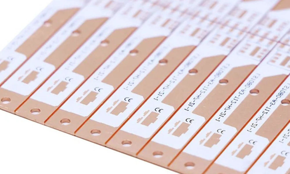
âComplex Assembly:ââ The board would host a mix of fine-pitch BGAs and sensitive analog components, demanding precise assembly and inspection.
âBEST Technology was selected to manufacture and assemble this critical board. The board’s specifications were meticulously chosen to meet the application’s demands.
âThis printed circuit board is designed as the main control board for a âportable medical diagnostic device. It is responsible for processing signals from various sensors, controlling the device’s user interface, and managing data communication. Its high reliability makes it suitable for critical applications in âpatient monitoring equipment, portable diagnostic analyzers, and other medical electronic devicesâ where consistent performance is non-negotiable.
âWe delivered the fully assembled and tested boards on schedule. Each unit passed our stringent quality checks, including AOI and X-ray inspection for BGAs. The comprehensive documentation package provided ensured a smooth and fast audit process for the client’s medical device certification. The project was a success, enabling the client to move seamlessly into the final testing and regulatory approval phase for their innovative product. This case underscores our commitment to providing ârigorous quality medical PCB assemblyâ for our clients in California and beyond.
âIn summary, PCB assembly Californiaâ is a critical service for the state’s innovative industries, particularly medical technology, where quality is non-negotiable. This guide has outlined the key considerations for selecting a manufacturing partner who can meet these high standards. BEST Technology stands out as a provider of ârigorous quality medical PCB assemblyâ by combining certified processes, engineering expertise, and a commitment to reliability. For a partner you can trust with your most critical projects, contact us at sales@bestpcbs.com.
RF Microwave PCBis a specialized circuit board designed for carrying and processing high-frequency signals, typically covering radio frequency (RF) from approximately 300 kHz to 300 GHz and microwave frequencies from 1 GHz to 300 GHz.
Unlike conventional PCBs, it utilizes high-frequency substrate materials such as Rogers, Teflon, or ceramic-filled composites. These materials feature extremely low signal loss, stable dielectric constant, and excellent thermal performance. Its design and manufacturing are highly precise, emphasizing signal integrity through exact control of trace impedance, optimized transmission line structures like microstrip and stripline, minimized parasitic effects, and strict regulation of laminate processes and surface treatments. This ensures efficient, low-distortion, and low-interference transmission of high-frequency or microwave signals on the board.
Why Choose RF Microwave PCB?
Benefits of RF Microwave Printed Circuit Board:
Stable High-Frequency Signal Transmission: Utilizes low-loss substrates and precise impedance control technology to support GHz-level high-frequency signal transmission. This reduces signal attenuation and crosstalk, ensuring signal integrity in high-speed scenarios such as 5G communications, radar, and satellite equipment, thereby enhancing the reliability of terminal products.
Reduced System Energy Consumption and Heat Dissipation Pressure: Optimizes circuit layout and high-performance dielectric materials like PTFE and ceramic-filled composites to achieve low insertion loss and efficient thermal management. This minimizes energy waste, lowers device heat generation, extends product lifespan, and reduces cooling module costs.
Compact Design for Miniaturization Needs: Enables high-density multi-layer routing to integrate complex RF modules. This allows precise arrangement of high-frequency components such as filters and amplifiers within limited space, meeting stringent miniaturization and lightweight requirements for smartphones, IoT devices, and other applications, boosting market competitiveness.
Superior Anti-Interference and Electromagnetic Compatibility: Incorporates shielding layers, optimized grounding, and electromagnetic simulation validation to effectively suppress high-frequency noise and external interference. This ensures stable device operation in complex electromagnetic environments like industrial control and automotive electronics, reducing failure rates and customer maintenance costs.
Accelerated Product Development Cycle: Standardized design processes and mature manufacturing techniques such as laser drilling and electroplating via filling shorten prototype verification and mass production timelines. Combined with Design for Manufacturability (DFM) guidance, this reduces trial production iterations, helping clients seize market opportunities and lower overall development costs.
Significant Long-Term Cost Efficiency: Although initial material and process costs are higher, the high reliability, low failure rate, and long-term stability result in reduced repair and replacement frequencies, lowering the total lifecycle cost. This makes it particularly suitable for high-reliability sectors like medical and aerospace applications.
1. Substrate Selection and Characteristic Matching
Material Expansion Selection: For high-frequency scenarios, recommend Rogers RO4350B, Taconic TLX series; for high-precision scenarios, select Panasonic Megtron 6 (Dk=3.3±0.05, lossïŒ0.002@10GHz) or Isola I-Tera MT40 (Dk=3.45, lossïŒ0.003@5GHz). FR-4 is limited to low-frequency test boards or cost-control scenarios, requiring gold-plating/immersion silver to reduce surface roughness impact.
Dynamic Parameter Verification: Use Agilent 85070D Dielectric Constant Tester to measure Dk values, combined with temperature-humidity aging tests to verify long-term stability. Thickness tolerance control requires collaboration with substrate supplier capabilities (e.g., ±5% high-end substrates), and design margin is increased to 25% to address processing errors.
Special Scenario Adaptation: Millimeter-wave (ïŒ30GHz) applications recommend Liquid Crystal Polymer (LCP) substrate (Dk=3.0, lossïŒ0.0015), paired with microvia arrays for ultra-low loss transmission.
TDR In-Depth Application: Set reference planes near TDR test points, measure single-ended/common-mode impedance via differential probes, and synchronously verify signal integrity metrics (rise timeïŒ20ps). For high-speed digital-RF hybrid circuits, use eye diagram instruments to validate timing margins.
Differential Pair Optimization: For serpentine differential pairs, validate bending radius impact on impedance via electromagnetic simulation, ensuring length matching errorïŒ0.5mil@10GHz.
3. Stack-Up Structure Optimization Design
Multilaminate Expansion Scheme: 8-layer boards recommend “Signal-GND-Power-Signal-Power-GND-Signal-Signal” structure with dual GND layers in the middle for dual shielding. 4-layer boards are only suitable for low-power RF modules, requiring blind/buried via technology for interlayer interconnection.
Interlayer Coupling Suppression: Insert low-dielectric isolation layers (e.g., Arlon AD300) between adjacent signal layers to reduce interlayer crosstalkïŒ20dB. Power-GND spacing is optimized via finite element analysis to ensure capacitance couplingïŒ90%.
Mixed-Signal Processing: For digital-RF hybrid circuits, use “island GND” technology to isolate digital noise, paired with beads/inductors to construct low-pass filter networks.
Via Optimization Design: Laser microvia technology achieves 0.1mm microvias, paired with back-drilling to eliminate stubs. High-frequency vias require parasitic parameter verification via Ansys Q3D to meet design thresholds.
Shielding Structure Upgrade: Set electromagnetic shielding walls around critical signal paths, using nickel/gold plating to enhance shielding effectiveness. For radiation-sensitive devices, use shielding covers + thermal gel composite heat dissipation solutions.
5. Grounding and Shielding Strategies
Hybrid Grounding Enhancement: Low-frequency modules use “star grounding” to the main ground terminal; high-frequency modules use “mesh grounding” to reduce ground bounce noise. RF front-end modules adopt “GND-Signal-GND” sandwich structure for dual shielding.
Shielding Effectiveness Verification: Use EMxpert near-field scanner to measure shielding effectivenessïŒ60dB@1GHz. Sensitive devices require 3D electromagnetic simulation to validate shielding structure effectiveness.
Ground Via Arrays: Adopt “honeycomb” via array layout with spacingâ€Î»/20@operating frequency to form a continuous Faraday cage. Vias require plating fill technology to enhance reliability.
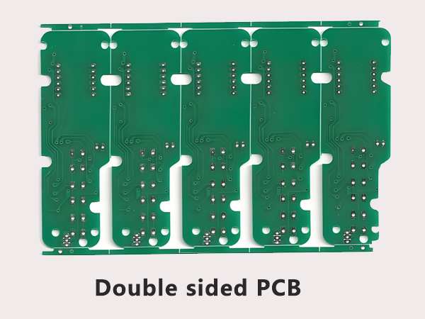
6. Power Integrity Optimization
Decoupling Capacitor Strategy: “0.01ÎŒF high-frequency + 10ÎŒF low-frequency” capacitor combinations paired with beads to construct multi-stage filter networks. Power noise-sensitive devices use embedded capacitor technology (e.g., buried capacitor layers).
Power Plane Optimization: Mesh copper pour enhances current carrying capacity, paired with thermal vias for thermal-electrical co-design. Power planes are validated via voltage drop simulation to ensure dropïŒ3%.
7. Thermal Management and Heat Dissipation Design
Heat Dissipation Structure Upgrade: High-power devices use “thermal pad + thermal via + heat sink” three-tier cooling solutions, paired with thermal interface materials to achieve thermal resistanceïŒ5â/W. Millimeter-wave devices use diamond heat sink substrates.
Thermal Simulation Verification: Use Ansys Icepak for thermal simulation to validate hotspot temperatureïŒ85â. For high-density layouts, use thermal-electrical-structural co-simulation to ensure thermal stressïŒmaterial yield strength.
Copper Thickness Selection: Top/bottom layers use 3oz copper for enhanced thermal diffusion; inner layers use 1oz copper to balance cost and performance. Extreme environment applications use gold-plating/immersion silver for corrosion resistance.

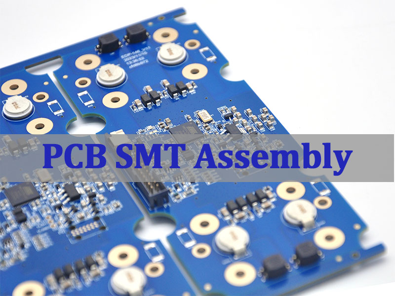
8. Design for Manufacturability and Testability
DFM Check Expansion: Includes line width uniformity, pad size consistency, minimum annular ring verification, etc. Use Valor NPI software for automated checks to meet IPC-6012 standards.
File Delivery Expansion: Includes complete Gerber files (impedance layer, pad layer, silkscreen layer, stencil layer) paired with process specification documents (back-drill depth, blind/buried via positions). Use Git version control for document traceability.
9. Simulation Verification and Document Delivery
Simulation Tool Expansion: Besides ADS/HFSS, use Keysight ADS Momentum for planar electromagnetic simulation or ANSYS HFSS 3D Layout for full-wave simulation. For time-domain response validation, use SPICE models paired with eye diagram instruments.
Document Package Enhancement: Includes design specifications, simulation reports, Gerber files, BOM lists, process specification documents, test reports, etc. Use PDF/A format for long-term readability, paired with digital signatures for tamper-proof validation.
Risk Management Strengthening: Use FMEA tools for risk assessment, clarify potential failure modes (crosstalk, hotspots, soldering defects) and solutions. Establish design change tracking systems to ensure all changes are validated and documented.
International Certification Assurance: Holds ISO 9001 quality management system certification and complies with industry-mandated certifications (e.g., medical, automotive, RoHS), ensuring product compatibility with global stringent application scenarios.
Free DFM Design Verification: Offers free Design for Manufacturability (DFM) analysis to identify and resolve potential design issues early, reducing development costs and risks while ensuring first-pass manufacturing success.
Competitive Pricing: Achieves cost control through optimized production processes and supply chain management, delivering cost-effective RF microwave PCB solutions particularly suitable for budget-sensitive projects.
24-Hour Rapid Prototyping: Supports sample production within 24 hours, enabling quick response to customer needs, shortened R&D cycles, and market opportunity capture, ideal for urgent project validation.
Flexible Low-MOQ and Small-Batch Production: Accepts low minimum order quantities (MOQ) and small-batch orders to meet R&D testing, small-scale production, or customization needs, reducing customer inventory pressure and capital tie-up.
Strict Full-Process Quality Control: Implements end-to-end quality control from raw material inspection, production monitoring, to final product testing, ensuring each PCB meets high reliability standards and minimizes defect rates.
Expert Technical Team Support: Features a team of experienced RF microwave engineers providing full-process technical support from design optimization and material selection to process adjustments to resolve complex technical challenges.
Efficient Supply Chain Management: Collaborates deeply with high-quality raw material suppliers to ensure stable material supply and rapid delivery, coupled with optimized production scheduling for on-time and reliable delivery.
Customized Service Capability: Offers tailored solutions for special requirements, including high-frequency material selection, impedance control optimization, and specialized surface treatments, to meet diverse project needs.
Responsive Customer Service: Provides 24/7 customer support for quick responses to inquiries, order tracking, and after-sales issues, delivering professional advice and solutions to enhance customer experience and trust.
Our RF Microwave PCB Capabilities
Parameter
Specification
Base material:
Rogers/Telfon
Board Thickness:
0.5mm~3.0mm(0.02″~0.12″)
Copper thickness:
0.5 OZ, 1.0 OZ, 2.0 OZ, 3.0 OZ
Outline:
Routing, punching, V-Cut
Soldermask:
White/Black/Blue/Green/Red Oil
Legend/Silkscreen Color:
Black/White
Surface finishing:
Immersion Gold, HASL, OSP
Max Panel size:
600*500mm(23.62″*19.68″)
Packing:
Vacuum/Plastic bag
Samples L/T:
7~9 Days
MP L/T:
8~10 Days
Our Quality Certification
ISO9001:2015: Universal quality management system covering design, production, and service. Enables continuous improvement via internal audits, KPI monitoring, and customer-centric processes.
ISO13485:2016: Medical device-specific certification focusing on lifecycle risk management, regulatory compliance, and supply chain traceability. Includes design validation, sterilization verification, and adverse event reporting.
RoHS: Environmental standard limiting 10 hazardous substances (e.g., Pb, Hg, Cd) in electrical/electronic equipment. Mandates homogeneous material testing and supplier declarations of conformity.
IATF16949: Automotive quality standard emphasizing defect prevention through APQP, PPAP, SPC, and FMEA. Ensures supply chain collaboration and customer-specific requirement compliance.
AS9100D: Aerospace quality system for safety-critical components. Mandates configuration management, design change traceability, NDT testing, and first article inspection (FAI) via ERP/MES systems.
How to Get A Quote for Your RF Microwave PCB Project?
Checklist for RF microwave PCB project quotations:
Layer and Structure: Specify layer count (e.g., 4/6/8 layers), board thickness (e.g., 1.0mm/1.6mm), and core layer positions.
Substrate Parameters: Indicate high-frequency substrate model (e.g., Rogers RO4350B), dielectric constant (Dk), and dissipation factor (Df).
PCB Switzerlandâ refers to the specialized ecosystem of companies within Switzerland that provide printed circuit board (PCB) manufacturing and assembly services. This article provides a comprehensive guide to selecting a reliable âPCB manufacturer Switzerland, highlighting the key factors for quality, certification, and how to achieve fast, flexible PCB solutions.
Are you struggling with Switzerland PCB suppliers who can’t adapt to your project’s unique demands or tight deadlines?
âSlow Prototyping Turnaround:ââ Lengthy lead times for prototypes hinder the R&D cycle and delay product time-to-market.
âInflexible Order Quantities:ââ Suppliers often impose high minimum order quantities (MOQs), making small-batch production or iterative testing cost-prohibitive.
âInconsistent Quality Control:ââ Failure to meet the stringent quality standards required by Swiss industries like medical, automotive, or aerospace.
âLimited Technical Support & Communication:ââ Difficulty in getting timely technical assistance or clear communication, leading to misunderstandings and errors.
âComplex Supply Chain Logistics:ââ Challenges in managing efficient and cost-effective shipping and customs clearance into Switzerland.
Fortunately, these challenges can be effectively mitigated by partnering with the right supplier. The solution lies in choosing a âPCB manufacturer Switzerlandâ that prioritizes agility and partnership.
âExpedited Prototyping Services:ââ Offering quick-turn PCB services, often with 24-72 hour lead times, to accelerate development.
âFlexible Ordering Options:ââ Providing low MOQs and on-demand production runs to support both prototyping and small-to-medium volume needs.
âRigorous Quality Assurance Systems:ââ Implementing multi-stage inspection protocols (e.g., AOI, Flying Probe Testing) and adhering to international standards.
âDedicated Customer Support:ââ Assigning knowledgeable project managers to provide expert guidance and ensure seamless communication.
âStreamlined Global Logistics:ââ Managing reliable shipping and handling customs documentation to ensure smooth delivery to your facility in Switzerland.
At BEST Technology, we are uniquely equipped to overcome these challenges. As a specialized âPCB manufacturerâ with a global footprint, we offer a comprehensive range of products, including FR4, Flexible Circuits, Rigid-Flex, Metal Core, and Ceramic PCBs. We pride ourselves on our client-first approach, which is reflected in our support for small-batch orders and our commitment to responding to all inquiries within 12 hours. By combining our diverse capabilities with an unwavering commitment to quality and speed, our core strength lies in delivering âquick PCB Switzerland with flexible solutionsâ that directly address your needs. Pls feel free to contact us at âsales@bestpcbs.comâ to discuss your PCB Switzerland project.
What is PCB Switzerland?
Fundamentally, “PCB Switzerland” signifies the solution for sourcing PCBs that meet the unparalleled standards of reliability and performance demanded by Swiss technology sectors. “PCB Switzerland” encompasses the local and international manufacturers serving the Swiss market, which is characterized by its demand for high-precision, high-reliability electronics in sectors like pharmaceuticals, finance, and watchmaking.
âA Hub for High-Reliability Electronics:ââ Swiss industries require PCBs that perform flawlessly under strict conditions, driving a focus on quality and precision.
âIntegration of Advanced Technologies:ââ It involves the use of cutting-edge materials and processes, such as HDI, rigid-flex, and ceramic PCBs, to meet sophisticated application needs.
âGlobal Sourcing with Local Standards:ââ While many physical âPCB manufacturer Switzerlandâ entities exist, the term also applies to international partners who are adept at meeting Swiss quality and logistical requirements.
In summary, PCB Switzerland represents a benchmark for excellence, where precision, reliability, and advanced technological integration are paramount.
Why Choose PCB Manufacturer Switzerland?
Selecting a manufacturer familiar with the Swiss market is crucial for project success. The primary reasons revolve around quality, precision, and supply chain efficiency.
âUnmatched Quality Standards:ââ Swiss manufacturers are synonymous with precision. Partnering with a âPCB assembly Switzerlandâ provider attuned to this culture ensures a commitment to zero-defect production.
âProximity and Logistics:ââ A local manufacturer or one with a streamlined European supply chain can significantly reduce shipping times and simplify logistics, contributing to quicker turnaround.
âUnderstanding of Compliance:ââ They are typically well-versed in the specific regulatory and compliance requirements (e.g., ISO 13485 for medical devices) critical for selling products in Switzerland and the broader EU.
Choosing a partner aligned with the “PCB Switzerland” ethos directly supports the goal of obtaining quick and reliable PCBs.
How Do PCB Assembly Switzerland Ensure Quality?
âPCB assembly Switzerlandâ providers guarantee quality through a systematic approach involving advanced technology, skilled personnel, and rigorous processes.
âAdvanced Inspection Technology:ââ They utilize Automated Optical Inspection (AOI) and X-ray inspection to detect soldering defects, component misalignment, and issues with BGAs or hidden joints.
âComprehensive Testing:ââ In-circuit testing (ICT) and flying probe testing are employed to verify electrical performance and ensure every circuit functions as designed.
âStrict Process Control:ââ Adherence to standardized processes like IPC-A-610 (Acceptability of Electronic Assemblies) is mandatory, covering everything from soldering quality to component placement.
This multi-layered quality assurance process is fundamental to delivering the reliable PCBs that the Swiss market demands.
What Certifications Should a PCB Switzerland Manufacturer Have?
Certifications are non-negotiable indicators of a manufacturer’s capability and reliability. A credible âPCB Switzerlandâ manufacturer should hold at least the following:
âISO 9001:ââ Demonstrates a robust Quality Management System.
âIATF 16949:ââ Essential for manufacturers serving the automotive industry.
âISO 13485:ââ A must-have for producing PCBs for medical devices.
âUL Listing:ââ Ensures the materials and boards meet recognized safety standards.
âAS9100:ââ The aerospace equivalent, indicating the highest level of quality control.
These certifications provide assurance that the manufacturer operates to internationally recognized standards.
How to Select Reliable PCB Switzerland Companies?
Selecting the right partner requires careful evaluation. Focus on these key criteria to find a reliable âPCB manufacturer Switzerland.
âEvaluate Technical Capabilities:ââ Review their experience with your required technology (e.g., multilayer, HDI, flex PCBs).
âAssess Communication and Support:ââ Gauge their responsiveness and the expertise of their support team during your initial inquiries.
âAnalyze Their Quality Data:ââ Request quality metrics like Defect Per Million (DPM) rates to objectively assess their performance.
âReview Their Logistics Expertise:ââ Ensure they have a proven track record of delivering to Switzerland without hassles.
âRequest and Evaluate Samples:ââ Before committing to a large order, order prototypes to personally assess the quality of their workmanship.
A thorough selection process minimizes risk and ensures a successful partnership.
Top 10 PCB Manufacturer Switzerland
The following list highlights the top 10 Swiss-based PCB manufacturers, each embodying the exceptional quality of “Swiss Made” craftsmanship.
1. ABB Circuit Ltd.
As a leader in the Swiss PCB industry and part of the ABB Group, ABB Circuit Ltd. brings profound expertise in industrial automation, energy management, and rail transportation. The company is renowned for its highly reliable, long-life PCB products, with particular proficiency in manufacturing multilayer and heavy-copper boards designed for harsh industrial environments.
2. Fischer Electronics AG
Based in central Switzerland, this electronics manufacturing services (EMS) provider enjoys an excellent reputation in the medical device and precision instrument sectors. Fischer Electronics specializes in low-volume, high-complexity PCB fabrication and assembly, ensuring its products meet the most stringent medical device quality standards.
3. Maxon Motor AG
While best known for its precision motors, Maxon also possesses advanced in-house PCB manufacturing capabilities dedicated to supporting its high-end motor drive systems. The company holds unique advantages in miniaturization and high-density interconnect (HDI) technology.
4. Mikron AG
With a century of experience, this company specializes in high-precision automation systems and precision components. Its PCB division primarily serves the medical technology and industrial automation sectors, boasting extensive experience in rigid-flex boards and high-temperature material applications.
5. Sefag AG
An important EMS provider in eastern Switzerland, Sefag holds a distinctive advantage in PCB manufacturing for the aerospace and defense industries. Its products are celebrated for their exceptional reliability and stability.
6. StÀubli Electrical Connectors AG
Although famous for its connectors, the company is also highly capable in specialty PCB manufacturing, particularly excelling in producing circuit boards for high-frequency, high-temperature, and other specialized application scenarios.
7. Zollikon Electronics AG
Located on the shores of Lake Zurich, this company focuses on PCB manufacturing for high-end measurement instruments and communication equipment, renowned within the industry for its expertise in fine-line circuit processing.
8. BĂ€r AG
As the largest EMS provider in western Switzerland, BĂ€r AG has accumulated rich experience in PCB manufacturing for automotive electronics and industrial control systems, with particular expertise in metal-core and high-temperature circuit boards.
9. St. Gallen Elektronik AG
Based in St. Gallen, this company has unique strengths in flexible and rigid-flex circuit board manufacturing, primarily serving the medical device and high-end consumer electronics markets.
10. Stotz Feinmechanik AG
Despite its origins in precision mechanics, the company also demonstrates outstanding capabilities in specialty PCB manufacturing, possessing deep expertise in producing specialized circuit boards for aerospace and high-end industrial applications.
Together, these Swiss-based PCB manufacturers form a high-end, specialized manufacturing ecosystem. While they may not focus on high-volume mass production, they offer irreplaceable value in terms of specialization, customization, and reliability. For high-end projects requiring the entire manufacturing process to be completed within Switzerland, these companies provide premium options that meet the “Swiss Made” standard, ensuring full traceability and quality consistency from design to production. Selecting the right partner requires careful consideration of how their specific expertise and technical strengths align with the project’s requirements.
Case of Supporting PCB Switzerland Project by EBest Circuit (Best Technology)
This advanced 6-layer HDI PCB serves as the core processing unit of a portable, high-precision blood analyzer. The device is designed for rapid point-of-care testing, providing doctors and medical staff with immediate diagnostic results. The board’s compact size allows for the handheld form factor, while its high-density interconnects and robust construction ensure reliable operation when moved between hospital rooms or used in mobile medical units. This is a Switzerland PCB project, reflecting the Swiss market’s uncompromising demand for precision, miniaturization, and reliability in medical technology.
âBoard Size:ââ 114.86mm x 156.81mm (4 pieces per panel)
âSolder Mask / Silkscreen:ââ Green LPI / White
âVia Treatment:ââ Via in Pad with epoxy filling and capping (VIPPO)
âQuality Deliverables:ââ Impedance test coupon and report included with shipment
By delivering a complex 6-layer HDI board with precise impedance control and reliable microvia structures, BEST Technology enabled the client to accelerate their development cycle while meeting the rigorous quality standards inherent to the Swiss medtech sector. The successful outcome underscores our commitment to providing âQuick PCB Switzerland with Flexible Solutions, proving that even the most demanding prototypes can be turned into reality with the right technical partnership. For your next high-stakes project, pls feel free to contact BEST Technology at âsales@bestpcbs.com.
Why Choose EBest Circuit (Best Technology) for Quick PCB Switzerland with Flexible Solutions?
BEST Technology is the ideal partner for your âPCB Switzerlandâ needs because we are built around the principles of speed and adaptability.
âRapid Response & Quick-Turn Production:ââ We prioritize prototype requests, offering industry-leading lead times to keep your projects on schedule.
âTrue Flexibility on Quantities:ââ We support orders from a single prototype to large-scale production, providing the agility your business needs.
âUncompromising Quality:ââ Our certified processes and advanced equipment ensure every board meets the highest standards of reliability.
âExpert Technical Collaboration:ââ Our engineers work closely with you to optimize designs and solve complex technical challenges.
âHassle-Free Logistics to Switzerland:ââ We manage the entire shipping process, ensuring your PCBs arrive on time and in perfect condition.
To conclude, âPCB Switzerlandâ signifies the pursuit of excellence in electronic circuit manufacturing and assembly, tailored to the high standards of the Swiss market. This guide has outlined the key considerations for navigating this specialized field. For âQuick PCB Switzerland with Flexible Solutions, BEST Technology stands ready to be your reliable partner, combining speed, quality, and exceptional service. For a quote or consultation, please contact us at âsales@bestpcbs.com.
PCB manufacturer Germanyâ refers to companies based in Germany that specialize in the production and assembly of Printed Circuit Boards (PCBs), offering a complete suite of services from fabrication to component sourcing and final box-build. This article explores the key advantages of partnering with a German PCB manufacturer, detailing the rigorous quality standards, essential certifications, and how to select the right partner for your project, with a specific focus on the comprehensive solutions provided by industry leaders.
Many businesses encounter significant obstacles when looking for reliable âPCB manufacturing companies in Germanyâ or elsewhere. These challenges include:
Inconsistent quality and frequent delays from suppliers.
High costs for low-volume prototype or specialized âflex PCB manufacturer Germanyâ services.
Complex logistics and communication barriers with overseas manufacturers.
Difficulty in finding expertise for advanced technologies like those offered by ârigid flex PCB manufacturers Germanyâ.
Lack of transparency and poor responsiveness throughout the âPCB manufacturing Germanyâ process.
âA trusted âPCB manufacturer in Germanyââ with a full turnkey approach can effectively eliminate these pain points. The solutions are clear and direct:
Implementing rigorous quality control systems to ensure consistency and on-time delivery.
Offering cost-effective prototyping and specialized manufacturing without sacrificing quality.
Providing local European support and streamlined logistics for seamless collaboration.
Possessing deep technical expertise in advanced PCB types, including rigid-flex and flex circuits.
Ensuring clear, continuous communication and project management from start to finish.
EBest Circuit (Best Technology) is a China-based PCB factory, and we have deep experience serving the European market. And we are committed to delivering precision, reliability, and exceptional service for projects of any scale. we solve key challenges by offering a one-stop solution for all your PCB needsâfrom standard FR4 and flexible circuits to sophisticated rigid-flex and metal core boards. We specialize in high-mix, low-volume production, ensuring you receive the highest quality, fastest possible delivery, and personalized service for your specialized projects. Pls feel free to contact us at sales@bestpcbs.com to discuss your requirements.
Why Choose PCB Manufacturer Germany?
Selecting a âPCB manufacturer Germanyâ based partner offers a distinct competitive advantage, particularly for industries where precision, reliability, and speed are non-negotiable. German engineering is synonymous with excellence, and this extends to its electronics manufacturing sector. This section outlines the primary benefits.
âUncompromising Quality Standards:ââ German âPCB manufacturers in Germanyââ adhere to the most stringent quality management systems. The culture of precision engineering ensures that every PCB meets exact specifications, resulting in higher reliability and longer product lifecycles.
âTechnical Expertise and Innovation:ââ Germany is a hub for R&D, especially in automotive, industrial automation, and medical technology. This environment fosters deep technical expertise among âPCB manufacturing companies in Germanyâ, particularly in advanced areas like HDI, high-frequency, and thermal management boards.
âSupply Chain Resilience and Proximity:ââ For companies within Europe, partnering with a local âPCB manufacturer in Germanyââ significantly shortens supply chains. This reduces logistical risks, lowers shipping costs, and allows for greater agility in responding to market changes or production adjustments.
âIP Protection and Regulatory Compliance:ââ Germany has robust intellectual property protection laws and strict environmental regulations (e.g., compliance with RoHS and REACH). Manufacturing your PCBs locally ensures your designs are secure and your products meet all necessary EU directives.
In summary, choosing a German PCB manufacturer is a strategic decision that prioritizes quality, innovation, and supply chain security, making it an ideal choice for high-value electronic products.
PCB Prototype Europe
The prototype phase is the critical bridge between design and mass production, where ideas are validated and potential issues are identified. For companies operating in the European market, utilizing a dedicated âPCB prototype Europeâ service is essential for accelerating development cycles, minimizing costs, and ensuring a smooth transition to volume manufacturing. A reliable prototype partner acts as an extension of your R&D team, providing not just boards, but valuable feedback.
âSpeed and Agility:ââ Leading European prototype services specialize in quick-turn production, offering turnaround times as fast as 24-48 hours for multilayer boards. This speed allows for rapid iteration and testing, keeping your project on an aggressive timeline.
âDesign for Manufacturing (DFM) Analysis:ââ A key value-add from a professional prototype house is a thorough DFM check. They analyze your design files to identify manufacturability issues, suggesting improvements to enhance yield, reliability, and performance before any metal is etched.
âAccess to Advanced Technologies:ââ A top-tier prototype service should offer the same advanced capabilities needed for production. This includes techniques like controlled impedance for high-speed designs, blind and buried vias for HDI layouts, and specific surface finishes like ENIG or ENEPIG.
Top Manufacturers for PCB Prototype in Europe:ââ
âBeta Layout (PCB Pool):ââ A well-known name for fast and cost-effective prototypes, particularly popular among hobbyists, engineers, and startups for their user-friendly online quotation and ordering system.
âEurocircuits:ââ A major European player with a strong focus on prototyping and small to medium series. They are recognized for their consistent quality, extensive online tools for DFM checks, and a wide range of standard technologies.
âMulticircuits:ââ Specializes in very fast turnaround prototypes and complex, high-specification boards, catering to clients who need high-reliability prototypes for demanding sectors like aerospace and defense.
In conclusion, selecting the right âPCB prototype Europeâ partner is a strategic decision. By prioritizing speed, engineering support, and technical capability, you can de-risk your project and ensure a seamless path to production with âPCB manufacturers in Germanyâ or other volume suppliers.
Rigid Flex PCB Manufacturers Germany
âRigid flex PCB manufacturers Germanyââ represent the pinnacle of PCB engineering, combining the stability of rigid boards with the flexibility of circuits. This technology is crucial for creating highly reliable, compact, and lightweight products in sectors like automotive, medical, and aerospace. German manufacturers are renowned for their precision and adherence to the strictest quality standards required for these complex assemblies.
âExpertise in Complex Stack-ups:ââ The core challenge is designing and laminating the rigid and flexible materials into a single, reliable structure. German engineers excel at managing the intricate layer stack-ups and material transitions to prevent delamination and stress fractures.
âPrecision Manufacturing Processes:ââ Production requires specialized equipment for controlled lamination cycles, precise laser drilling of microvias on flex areas, and accurate coverlay application. Process control is paramount to ensure reliability under dynamic flexing conditions.
âRigorous Testing and Validation:ââ Given their use in critical applications, rigid-flex boards undergo extensive testing far beyond standard PCBs. This includes continuity testing during and after dynamic flexing, cross-sectional analysis, and environmental stress testing (thermal cycling, humidity).
Top Rigid-Flex PCB Manufacturers in Germany:ââ
âWĂŒrth Elektronik:ââ A global giant and one of the leading âGermany PCB manufacturers, WĂŒrth has deep expertise in rigid-flex technology. They offer full support from design to volume production, serving automotive, industrial, and medical markets.
âSchweizer Electronic AG:ââ Known for its innovation in advanced PCB technologies, Schweizer specializes in complex solutions including sophisticated rigid-flex designs for high-power and high-frequency applications, particularly in the automotive sector.
âKSG GmbH:ââ A specialized manufacturer focused on high-end multilayer, HDI, and rigid-flex PCBs. They are known for their engineering support and ability to produce highly complex, low-volume boards for specialized applications.
In summary, partnering with experienced ârigid flex PCB manufacturers Germanyâ is essential for leveraging this advanced technology. Their methodical approach to design, material science, and rigorous quality assurance ensures the final product meets the highest performance and reliability standards.
Flex PCB Manufacturer Germany
A specialized âflex PCB manufacturer Germanyââ focuses on the unique demands of single-sided, double-sided, and multilayer flexible circuits. These PCBs enable modern product design by allowing three-dimensional packaging and continuous motion. German manufacturers bring a level of precision and quality control that is critical for producing durable and reliable flex circuits.
âMaterial Selection and Handling:ââ Expertise begins with selecting the appropriate polyimide or other flexible films, adhesives, and coverlays. Proper handling throughout the manufacturing process is critical to prevent scratches, creases, or tears in the delicate materials.
âPrecision Etching and Coverlay Application:ââ Achieving fine traces on flexible substrates requires specialized etching processes. The application of the protective coverlay must be precise to expose pads correctly while providing robust protection, often done using photolithographic methods for accuracy.
âSpecialized Assembly Processes:ââ Assembling components onto flex circuits requires specific processes, such as using specialized fixtures (palletization) to support the board during soldering and careful control of thermal profiles during reflow to prevent damage to the flexible material.
Top Flex PCB Manufacturers in Germany:ââ
âFlexible Circuit Technologies (FCT):ââ While international, they have a strong presence and are a major specialist in flexible circuit design and manufacturing, offering services from simple flex circuits to complex multilayer assemblies.
âAT&S Austria:ââ Although based in Austria, AT&S is a leading European PCB manufacturer with significant operations and influence in the DACH region (Germany, Austria, Switzerland), producing high-end flexible circuits for the automotive and consumer electronics industries.
âMeyer-BMC:ââ A German-based company specializing in flexible and rigid-flex PCBs, offering design support and manufacturing services tailored to the needs of various industrial sectors.
In conclusion, a proficient âflex PCB manufacturer Germanyâ provides more than just fabrication; they offer essential guidance on design rules for flexibility, material choices for specific environments, and assembly techniques that guarantee the longevity and performance of the final flexible circuit assembly.
How Do PCB Manufacturers in Germany Ensure Quality?
Quality is not an accident but a result of systematic processes. âPCB manufacturers in Germanyâ ensure quality through a multi-layered approach:
âAutomated Optical Inspection (AOI):ââ Every layer and the final assembled board is scanned by high-resolution cameras to detect defects like shorts, opens, or incorrect component placement.
âElectrical Testing:ââ 100% electrical testing (Flying Probe or Bed-of-Nails) is performed to verify netlist continuity and isolate shorts.
âIn-Process Controls:ââ Quality checks are integrated throughout the entire âPCB manufacturing Germanyâ process, from material inspection to solder paste printing and reflow profiling.
âX-Ray Inspection:ââ Used to examine hidden connections, such as Ball Grid Array (BGA) soldering and internal layers of multilayer boards.
âIPC Standards Compliance:ââ Adherence to IPC-A-600 (acceptability of printed boards) and IPC-A-610 (acceptability of electronic assemblies) is standard practice, ensuring the final product meets international quality benchmarks.
In conclusion, PCB manufacturers in Germany uphold their reputation through meticulous inspection, advanced testing, and strict adherence to global standards. This disciplined quality management guarantees that every circuit board delivers long-term reliability and performance, even in the most demanding applications.
What Certifications Should a PCB Manufacturer in Germany Have?
Certifications provide independent verification of a manufacturer’s capabilities and commitment to quality. A reputable âPCB manufacturer in Germanyâ should hold, at a minimum, the following certifications:
âISO 9001:ââ The international standard for Quality Management Systems, ensuring consistent quality and continuous improvement.
âIATF 16949:ââ Essential for suppliers to the automotive industry, demonstrating a focus on defect prevention and waste reduction.
âISO 13485:ââ For medical device manufacturing, emphasizing risk management and traceability throughout the production process.
âUL Certification:ââ Underwriters Laboratories certification, often required for PCBs used in North American markets, verifying the safety of the materials and construction.
âAS9100:ââ The aerospace equivalent of ISO 9001, requiring stringent controls for the highly regulated aerospace industry.
These certifications are a clear indicator that the manufacturer operates under a certified management system capable of delivering high-quality products.
How to Select Trusted PCB Manufacturing Companies in Germany?
Selecting the right partner from the many âPCB manufacturing companies in Germanyââ requires careful evaluation. Follow this structured approach:
âAssess Technical Capabilities:ââ Review their portfolio for experience with your specific technology (e.g., layer count, flex/rigid-flex, high-speed).
âEvaluate Quality Certifications:ââ Confirm they hold the relevant certifications for your industry (as listed above).
âRequest DFM and Support:ââ A good partner will offer proactive DFM support. Gauge their responsiveness and willingness to collaborate on optimizing your design.
âAnalyze Communication and Transparency:ââ Ensure they assign a dedicated project manager and provide clear communication channels and regular updates.
âConsider Scalability and Logistics:ââ Verify that they can scale from prototype to mass production and have efficient logistics solutions for delivering to your location.
By systematically checking these boxes, you can identify a manufacturer that is not just a supplier but a true strategic partner.
Case of Supporting PCB Manufacturing Germany Project by EBest Circuit (Best Technology)
EBest Circuit (Best Technology), a leading PCB manufacturer from China with extensive experience serving the German industrial and medical sectors, provides high-reliability printed circuit boards for critical applications. Our PCBs are integral to the performance of advanced medical devices, such as the compact patient monitors used in Germany.
The PCBs supplied by EBest Circuit (Best Technology) are engineered for a compact patient monitoring system designed for use in various clinical settings, including intensive care units (ICUs), emergency rooms, and general wards. This device provides comprehensive vital sign tracking for adult, pediatric, and neonatal patients. It requires PCBs that ensure exceptional reliability, signal integrity, and durability to support continuous monitoring, high-resolution data processing, and long battery life.
âSupporting PCB Manufacturing Capabilitiesâ
To meet the stringent demands of this medical application, our manufacturing process leverages specific capabilities that guarantee the performance and safety of the final product. Key capabilities relevant to this project include:
âHigh-TG Materials:ââ We utilize FR4 materials with high Glass Transition temperature (Tg >170°C), ensuring board stability and reliability during continuous operation and potential thermal stress.
âAdvanced Layer Count:ââ Our expertise in manufacturing multilayer boards up to 32 layers allows for the complex routing and high-density integration required for the monitor’s sophisticated internal modules.
âControlled Impedance:ââ We maintain precise control over line width and spacing (e.g., 3/3 mil for 1oz copper), which is critical for the accurate signal integrity needed for ECG and respiration monitoring.
âReliable Surface Finish:ââ We offer Immersion Gold (ENIG) as a standard, robust finish, providing a flat surface for reliable connections and excellent solderability for the monitor’s components.
âFine Line Technology:ââ Our capability to produce fine lines and spaces supports the high-density interconnects (HDI) necessary for the compact design of the monitor’s main and auxiliary boards.
âStrict Tolerances:ââ We adhere to tight fabrication tolerances for hole diameter (±2mil for NPTH) and layer-to-layer registration, ensuring perfect fit and function within the device’s assembly.
âMedical-Grade Compliance:ââ Our processes are geared towards meeting the high-quality standards (such as high CTI values for better leakage current protection) demanded by the medical industry.
By integrating these precise manufacturing capabilities, EBest Circuit (Best Technology) delivers PCBs that form the reliable core of advanced medical monitoring systems, contributing to accurate diagnostics and enhanced patient care.
Why Choose EBest Circuit (Best Technology) for PCB Prototype and Turnkey PCB Assembly?
EBest Circuit (Best Technology) stands out among PCB manufacturers by offering a truly integrated, full turnkey solution. We manage the entire processâfrom PCB fabrication and component procurement to assembly, testing, and final shipmentâunder one roof. This eliminates the complexity and risk of coordinating with multiple vendors.
ââWide Range of PCB Typesââ
We support diverse PCB needs including FR4, Metal Core (MCPCB), Ceramic, Flexible, Rigid-Flex, Heavy Copper, High-Frequency, and Special PCBsâhandling both prototypes and small to medium batch production.
ââSmall Batch & No MOQ Supportââ
Whether you need a single prototype or small-volume orders, we welcome projects of any size with no minimum order quantity (MOQ), offering flexibility for R&D and pilot runs.
ââHigh Quality & Reliable Certificationââ
With ISO9001, IATF16949, ISO13485, RoHS, and REACH certifications, we implement strict quality control and IPC standards throughout production to ensure superior reliability and performance.
ââFast Delivery & Quick Responseââ
We provide expedited servicesâwith prototype lead times as short as 24 hoursâand assign dedicated engineering support to ensure timely updates and on-time delivery, keeping your project on schedule.
ââExcellent Full Turnkey Serviceââ
From design and DFM support to component sourcing, PCB assembly, and final box-build, we deliver end-to-end solutions with one-on-one customer service, ensuring a smooth and collaborative experience.
Our expertise in advanced PCB technologies, combined with a customer-first approach, makes us the ideal partner for innovative and demanding PCB manufacturing Germanyâprojects. We ensure a smooth, efficient journey from your initial concept to a fully assembled, high-quality product delivered to your door.
âAll in all, PCB manufacturer Germanyâ represents a benchmark for quality, precision, and reliability in the electronics manufacturing industry. This guide has detailed the key reasons to choose a German partner, from their technical expertise to their robust quality systems. For businesses seeking a seamless, full turnkey assembly service, partnering with an experienced and capable manufacturer is crucial. At EBest Circuit (Best Technology), we embody these principles, offering expert guidance, state-of-the-art manufacturing, and a commitment to partnership on every project. Let us help you bring your next electronic innovation to life. Contact our team today at sales@bestpcbs.com to get started.
How to calculate PCB dielectric thickness? Let’s discover common thickness and IPC standard, calculation and measurement methods, design consideration, application cases for PCB dielectric thickness.
Are you worried about these problems?
Does dielectric thickness deviation always cause impedance & signal quality issues to surface only in final testing?
Is uneven thickness post-multilaminate consistently dragging down your product yield?
Are vague thickness control commitments from suppliers dragging your project cycles into endless confirmation loops?
As a PCB manufacturer, EBest Circuit (Best Technology) can provide you service and solution:
Precision Thickness Control: Commit to ±3Όm tolerance with real-time thickness mapping for proactive impedance prediction during design.
Transparent Data Traceability: Build dedicated digital thickness archives per order, online access, full process transparency, zero guesswork.
Welcome to contact us if you have any request for PCB design, prototyping, mass production and PCBA service: sales@bestpcbs.com.
What Is PCB Dielectric Thickness?
PCB dielectric thickness refers to the vertical distance of the insulating material between adjacent conductive layers, such as signal layers, power planes, or ground planes, typically measured in millimeters (mm). It is a critical parameter in PCB stackup design, directly impacting electrical performance (e.g., impedance control, signal integrity) and mechanical stability.
Industry standards generally recommend a minimum dielectric thickness of 0.1mm to prevent voltage breakdown, while emphasizing symmetric design principles, including consistency in dielectric material type, copper foil thickness, and pattern distribution to ensure board reliability.
Common PCB Dielectric Thickness
Single-Sided PCBs
Thickness Range: 0.2mm (8mil) to 1.6mm (63mil), with 1.0mm (39mil) being most common for cost-sensitive applications.
Design Rules: Minimal dielectric thickness â„0.1mm to prevent voltage breakdown; no symmetry requirement due to single conductive layer.
Applications:Simple control circuits, LED displays, and entry-level consumer electronics.
2 Layer PCBs
Thickness Range: 0.2mm (8mil) to 1.6mm (63mil), with 1.0mm (39mil) and 1.6mm (63mil) dominating industrial/consumer markets.
Features: Symmetric dielectric layers (e.g., 0.8mm core + 0.1mm prepreg on each side) ensure mechanical stability; supports through-hole vias.
Applications: Power supplies, automotive electronics, and mid-complexity control systems.
4 Layer PCBs
Stack-Up Example: Top/bottom signal layers (0.5mm core each), inner power/ground layers (0.2mm core), separated by 0.1mm prepreg. Total thickness â1.0mm.
Applications:Smartphones, IoT devices, and compact industrial controllers.
6/8-Layer and Higher Multilayer PCB
Thickness Allocation: Core layers (0.1mmâ0.3mm), prepreg layers (0.05mmâ0.2mm), with incremental layer addition. For example, an 8-layer board may use dual 0.2mm cores + multiple 0.1mm prepregs.
Advanced Design: High-speed/high-frequency applications adopt ultra-thin dielectrics (â€0.075mm) and low-loss materials (e.g., Rogers RO4003C at 0.1mm) for RF/5G modules.
Material parameter refinement: FR-4 exhibits Δ_r = 4.5â4.8 at 1GHz, while high-frequency materials like RO4350B show Δ_r = 3.66 ± 0.05 at 10GHz.
Copper thickness calibration: 1oz copper measures 35Όm ± 2Όm, with etching factor ~0.8 accounting for sidewall taper.
Iterative solving: Numerical methods like Newton-Raphson or bisection are recommended, leveraging built-in algorithms in tools like Altiumâs impedance calculator.
2. Professional Tools and Software Applications
EDA Tool Extensions:
Altium Designer: supports differential pair impedance scanning, stackup sensitivity analysis, and 3D EM simulation validation.
Cadence Allegro: integrates Sigrity for signal integrity analysis, enabling power plane decoupling capacitor optimization.
Mentor PADS: offers rapid stackup estimation tools with material library imports for PP sheet matching.
Note: Peeling may cause dielectric layer tearing, affecting measurement accuracy.
2. Non-destructive Measurement
Laser Thickness Gauge
Principle: Laser triangulation/interferometry, calculates thickness via optical path difference.
Advantages: Accuracy ±0.5 ÎŒm, supports 0.15â0.25N micro-pressure contact to prevent board deformation, measures local areas of multilayer boards (e.g., under impedance lines).
Typical Equipment: Oxford CMI series (95% industry coverage), integrates micro-resistance (SRP-4) and eddy current (ETP) technologies for simultaneous copper thickness measurement.
X-ray Fluorescence (XRF)
Application: Irradiate copper-clad laminate with X-rays â Analyze characteristic X-ray energy/intensity â Derive dielectric thickness (requires known material composition).
Automation: Regional scanning with 100+ measurement points per area, SpecMetrix system achieves <1ÎŒm error (vs. cross-section method).
Principle: High-voltage probes (4â8 pins) test insulation resistance â Calculate thickness via known dielectric constant (Dk) model (Formula: H â ln(insulation resistance)/Dk)
Advantages: No fixture required, supports 0.2mm micro-pitch testing, suitable for high-density boards
Limitations: Relies on Dk value accuracy (may drift in millimeter-wave bands)
At high frequencies, the impact of dielectric loss tangent (Df) becomes significant. FR-4 has a Df of ~0.018, resulting in 0.3dB/cm loss at 10GHz; whereas Rogers 4350B, with Df of 0.003, reduces loss to 0.05dB/cm at the same frequency. For 5G millimeter-wave designs (28GHz), 0.08mm PTFE substrate reduces insertion loss by 30% but requires increased glass fiber density to prevent dielectric constant fluctuations.
Lamination Symmetry Engineering Practice:
A typical symmetric 8-layer stackup is: Top layer – 0.05mm dielectric – Ground plane – 0.2mm dielectric – Power plane – 0.05mm dielectric – Bottom layer. This structure matches CTE (coefficient of thermal expansion), limiting warpage to 0.5%. Asymmetric designs, such as 0.3mm dielectric used unilaterally, cause Z-axis CTE differences exceeding 50ppm/â, risking pad cracking.
Voltage Withstand & Insulation Enhancement:
For IGBT driver boards, 0.4mm PPO substrate withstands 1.2kVrms voltage, and with 2mil copper foil achieves 10kV breakdown voltage. Edge effects require chamfering (Râ„0.5mm) and potting compound (Δr=3.5) to reduce field strength by 40%, meeting UL94V-0 flame retardancy.
Thermal Management Synergy Design:
In power modules, 0.3mm thermal substrate (e.g., T410) with 2oz copper thickness controls thermal resistance at 0.8â/W. Combined with thermal via arrays (50 vias/cmÂČ density), junction temperature reduces by 20â. CTE matching must be ensured to avoid thermal stress cracking from copper-substrate differences.
Mechanical Stability Enhancement:
Aerospace PCBs require vibration resistance >20G. Using 0.5mm substrate with back-copper reinforcement raises natural frequency to 120Hz, exceeding typical vibration spectra (5-100Hz). Finite element analysis (FEA) optimizes stiffener layout, reducing stress concentration by 50%.
Material Availability & Cost Control:
Standard FR-4 thickness (0.1-0.2mm) shows 15% cost variance, while 0.08mm ultra-thin substrate requires customization, extending lead time by 3 weeks. Hybrid stackups (e.g., 0.2mm FR-4 + 0.1mm high-speed material) balance performance and cost but require attention to lamination temperature differences to prevent delamination.
Manufacturing Process Limit Breakthrough:
mSAP technology achieves 0.05mm dielectric thickness with ±2% tolerance, requiring vacuum laminators (±1% pressure accuracy) and optical inspection (1Όm resolution). For HDI designs, 0.03mm dielectric uses laser microvias (50Όm diameter) with electroplated fill to ensure reliability.
How Does Dielectric Layer Thickness Affect PCB Performance?
High-Speed Signal Quality: In high-frequency (>5GHz) scenarios, thickness variations exacerbate signal delay and loss. At 10GHz, a 1.6mm board exhibits 33% higher loss (0.8dB/cm) than a 1.0mm board, impacting eye diagram opening (e.g., USB3.0 design requires strict thickness tolerance control).
Crosstalk and EMI: Thin dielectrics (e.g., 3-5mil) increase capacitive coupling between adjacent signal lines, raising crosstalk risk. Thicker boards reduce same-layer crosstalk by increasing layer spacing but require higher ground via density to prevent inter-layer crosstalk.
Thermal Management and Heat Dissipation
Thermal Conductivity Efficiency: Copper foil (385W/m·K thermal conductivity) serves as the primary thermal channel. Thick copper (e.g., 2oz) combined with 1.6mm substrate improves heat dissipation by 50%, reducing chip junction temperature (e.g., 20W chip junction temp drops from 83°C to 68°C).
Thermal Resistance Balance: Substrate thickness has an optimal range, 1.6mm boards show lower total thermal resistance (0.6°C/W) than 1.0mm (0.8°C/W). Beyond 2.0mm, substrate thermal resistance offsets copper gains, reducing effectiveness.
Uniformity and Reliability: Thick substrates (>1.6mm) enhance thermal capacity, slowing temperature rise and reducing hotspots (e.g., 60% smaller hotspot area), extending component life.
Mechanical Strength and Durability
Bending Resistance: Thick boards (â„1.6mm) offer higher mechanical rigidity, suitable for industrial/automotive applications requiring mechanical stress resistance. Thin boards (<1.0mm) are prone to bending, requiring stiffeners or flexible designs (e.g., polyimide substrates).
Thermal Expansion Matching: Z-axis CTE increases with thickness and must match components (e.g., ceramic chip CTE 5ppm/°C) to prevent solder joint cracking (e.g., 1.6mm board CTE 65ppm/°C outperforms 2.4mm board 75ppm/°C).
Manufacturing Process and Cost
Process Limitations: Ultra-thin dielectrics (<3mil) are challenging to manufacture, requiring prepreg materials for consistency. Thick boards need specialized lamination/drilling techniques, increasing costs.
Cost Tradeoffs: Thick copper and high-performance substrates (e.g., PTFE) improve performance but raise costs. Balancing signal integrity, thermal needs, and budget is essential.
EMC and Environmental Adaptability
Shielding Effectiveness: Thick boards enhance EMI suppression by increasing ground plane spacing, combined with 20H/3H principles (power plane inset 20H, signal line spacing 3H) to reduce edge radiation.
Environmental Tolerance: Thin boards are sensitive to humidity/temperature, requiring protective coatings. Thick boards offer better thermal stability in extreme temperatures but must avoid thermal stress-induced delamination.
Welcome to contact us if you need any help for PCB dielectric thickness: sales@bestpcbs.com.
This website uses cookies to enhance your experience, remember your preferences, and help us understand how visitors use our site. You can accept all cookies, reject non-essential cookies, or manage your settings.
This website uses cookies to improve your experience while you navigate through the website. Out of these cookies, the cookies that are categorized as necessary are stored on your browser as they are essential for the working of basic functionalities of the website. We also use third-party cookies that help us analyze and understand how you use this website. These cookies will be stored in your browser only with your consent. You also have the option to opt-out of these cookies. But opting out of some of these cookies may have an effect on your browsing experience.
Necessary cookies are absolutely essential for the website to function properly. These cookies ensure basic functionalities and security features of the website, anonymously.
Cookie
Duration
Description
cookielawinfo-checkbox-analytics
11 months
This cookie is set by GDPR Cookie Consent plugin. The cookie is used to store the user consent for the cookies in the category "Analytics".
cookielawinfo-checkbox-functional
11 months
The cookie is set by GDPR cookie consent to record the user consent for the cookies in the category "Functional".
cookielawinfo-checkbox-necessary
11 months
This cookie is set by GDPR Cookie Consent plugin. The cookies is used to store the user consent for the cookies in the category "Necessary".
cookielawinfo-checkbox-others
11 months
This cookie is set by GDPR Cookie Consent plugin. The cookie is used to store the user consent for the cookies in the category "Other.
cookielawinfo-checkbox-performance
11 months
This cookie is set by GDPR Cookie Consent plugin. The cookie is used to store the user consent for the cookies in the category "Performance".
viewed_cookie_policy
11 months
The cookie is set by the GDPR Cookie Consent plugin and is used to store whether or not user has consented to the use of cookies. It does not store any personal data.
Functional cookies help to perform certain functionalities like sharing the content of the website on social media platforms, collect feedbacks, and other third-party features.
Performance cookies are used to understand and analyze the key performance indexes of the website which helps in delivering a better user experience for the visitors.
Analytical cookies are used to understand how visitors interact with the website. These cookies help provide information on metrics the number of visitors, bounce rate, traffic source, etc.
Advertisement cookies are used to provide visitors with relevant ads and marketing campaigns. These cookies track visitors across websites and collect information to provide customized ads.