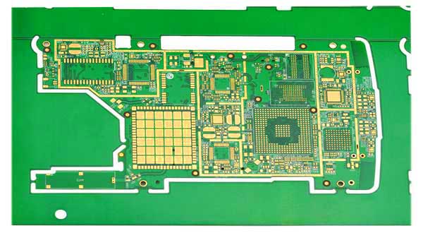
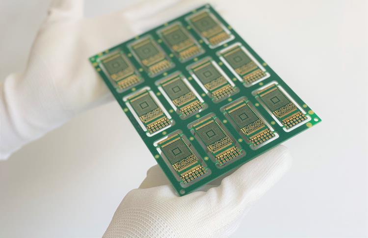
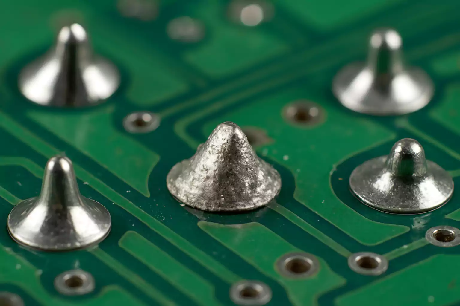
If you’ve ever worked with Metal Core PCBs (MCPCBs), or copper-clad boards, you’ve likely appreciated their superb ability to whisk heat away from powerful components like LEDs or power converters. But this very strength introduces a unique and frustrating weakness: the dreaded pad lift.
There’s little more disheartening than seeing a copper pad, along with your carefully soldered component, physically peel away from the board during assembly or rework. This isn’t a simple soldering mistake; it’s a fundamental battle between physics and materials that you lost. But it’s a battle you can win.
This blog post will dive deep into the why and, more importantly, the how—how to prevent this costly issue from plaguing your projects.
What Cause Pads Lift on Copper-Clad Boards?
To understand why pad lifting happens, we must first look at the structure of a typical Copper MCPCB:
1. Copper Circuit Layer: The thin layer where your traces and pads are etched.
2. Dielectric Insulating Layer: A critical polymer-based layer (often epoxy with ceramic fillers) that electrically isolates the circuit from the metal base. It’s also the primary thermal conduit.
3. Copper or Aluminum Base Plate: The thick metal core that acts as a massive heat sink.
The problem lies in their Coefficients of Thermal Expansion (CTE). Copper and aluminum have very similar CTEs. The dielectric layer, however, has a CTE that is vastly different. When you subject the board to the high temperatures of a soldering process (200-260°C+), these layers expand at dramatically different rates.
Upon cooling, they contract at different rates again. This mismatch creates immense shear stress right at the interface between the copper pad and the dielectric layer. When this internal stress exceeds the adhesive strength (the “peel strength”) bonding the copper to the dielectric, the pad delaminates and lifts off.
This fundamental CTE mismatch is a given. The goal, then, is to manage the forces and strengthen the system to prevent failure.
What Actually Pushes a Pad to Lift?
Several factors in design, manufacturing, and assembly act as the “last straw” that triggers a pad lift.
1. Thermal Shock During Assembly & Rework This is, by far, the number one cause.
Excessive or Prolonged Rework: Every time you apply a soldering iron to a pad, you create a localized, extreme thermal cycle. The pad heats up and expands rapidly, while the surrounding area remains cooler. Multiple rework attempts fatigue the bond, progressively weakening it until it fails. The higher the iron temperature and the longer the contact time, the greater the risk.
Incorrect Soldering Iron Use: Using an overpowered iron, a tip that’s too small (forcing you to hold it longer), or applying excessive pressure to “squeeze” heat out, all contribute to thermal shock and mechanical damage.
Aggressive Reflow Profiles: An oven profile with too high a peak temperature or excessive time above liquidus can “cook” the dielectric layer, weakening its adhesive properties across the entire board.
2. PCB Design Flaws The board’s layout can set the stage for failure from the very beginning.
Poor Thermal Relief Design: A pad directly connected to a large copper pour for thermal management acts as a massive heat sink. To melt the solder, you must pump in far more heat for a longer duration, dramatically increasing the thermal stress on the pad’s connection point. This is the most common design-related mistake.
Isolated Pads: Conversely, a pad with no thermal connection can heat up too quickly, creating a severe thermal gradient and concentrating stress upon cooling.
3. PCB Manufacturing Quality Not all MCPCBs are created equal.
Low Peel Strength: The core specification for pad adhesion is the Copper Foil Peel Strength. Low-quality laminates simply have inferior bonding between the copper and the dielectric layer, offering less resistance to the inherent thermal stress.
Drilling and Fabrication Issues: Poor drilling quality can cause micro-fractures or delamination around via holes, creating a weak point from which a pad can start to lift.
4. Mechanical Stress Physical forces can work in tandem with thermal stress to finish the job.
Installation Stress: Over-tightening the screws when mounting the MCPCB to a heatsink can warp the board. This pre-stresses the copper-dielectric bond, making it much more susceptible to failure during the subsequent soldering heat cycle.
Component Stress: Heavy components or components with stiff leads can exert constant mechanical leverage on the pads, especially under vibration.
How to Prevent Pad Lifting?
Fixing pad lifting requires a systematic approach across design, sourcing, and assembly.
1. Master the Soldering Process (The Most Critical Step)
Control Time and Temperature: Use a temperature-controlled iron. Set it to the lowest effective temperature (typically 350-380°C for lead-free solder) and adhere to the “3-to-5 Second” rule: complete the joint within 3 seconds, and never exceed 5 seconds of continuous contact.
Limit Rework: Establish a strict limit—if a joint isn’t right after 2-3 attempts, stop. Let the board cool completely and re-evaluate your approach. Forcing it will only lead to failure.
Use the Right Tool: Match your soldering tip size to the pad and component. A larger, chisel tip transfers heat more efficiently than a fine point, reducing the time needed.
2. Implement Smart PCB Design
Use Thermal Relief Pads (The Golden Rule):This is the single most effective design change. Instead of connecting a pad directly to a copper plane, use a “spoked” or “cross-hatched” connection. These thin traces provide sufficient electrical and thermal conductivity while significantly increasing the thermal resistance during soldering. This allows the pad to heat up quickly without stealing all the heat away, minimizing the thermal stress.
Reinforce Pads: Use teardrops at the junction of pads and traces to add mechanical strength. Where possible, slightly increase the pad size to improve adhesion.
3. Source High-Quality Materials
Specify High Peel Strength: When ordering your MCPCBs, don’t just shop for price. Consult with your manufacturer and specify a material with a high copper peel strength. Reputable laminate suppliers (like Bergquist or Laird) provide these specifications.
Audit Your PCB Supplier: Work with a fabricator who has proven experience with MCPCBs and understands the rigorous demands of the assembly process.
4. Refine Mechanical Assembly
Control Torque: Use a torque screwdriver when mounting the board to a heatsink. Follow the manufacturer’s recommended torque values and tightening sequence to avoid warping.
Support Heavy Components: For large parts, use adhesive or additional mechanical fasteners to secure the component body, relieving the strain on the solder joints and pads.
Conclusion
Pad lifting on MCPCBs isn’t random. It’s the result of predictable stress acting on a thin copper-dielectric interface. When that stress rises above the material’s peel strength, the pad lets go.
But you can prevent it.
Solder smarter with tight control of heat and dwell time.
Use thermal relief features in your design.
Choose MCPCB materials with high peel strength.
Avoid mechanical stress during assembly.
Once you align your design, materials, and soldering process with the thermal realities of MCPCBs, your pad-lifting issues drop dramatically—and your yield, reliability, and confidence rise just as quickly.
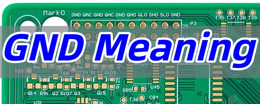
GND meaning is foundational in electronics, referring to the ground reference point that ensures stable circuit operation. This article explores the role of GND in circuits, clarifies common misconceptions, and provides practical guidance to avoid grounding errors.
Grounding mistakes can lead to circuit failure, noise interference, or even safety hazards. Whether you’re designing a PCB or troubleshooting a device, understanding GND is critical.
Why do so many engineers struggle with GND circuits?
Unstable Signals: Noise and voltage fluctuations due to poor grounding.
Confusion Between GND Types: Mixing analog, digital, and chassis grounds.
Faulty Reference Points: Incorrect zero-volt reference leading to measurement errors.
Safety Risks: Inadequate grounding resulting in electric shocks or device damage.
To address these issues, follow these key solutions:
Implement star grounding to isolate noise-sensitive circuits.
Use continuous GND planes in PCB design to reduce impedance.
Clearly separate PGND (power ground) and SGND (signal ground).
Define a single-point reference for voltage measurements.
Ensure proper chassis grounding for safety compliance.
At BEST Technology, we specialize in advanced PCB manufacturing, offering robust solutions for complex grounding challenges. Our expertise ensures your designs achieve optimal performance and reliability. Pls feel free to contact us at sales@bestpcbs.com for professional support.
What Does GND Mean?
GND meaning stands for “ground,” the reference point in a circuit where voltage is zero. It serves as a common return path for current and a benchmark for measuring voltages elsewhere in the system.
In electronics, GND is not just a physical connection to the earth—it’s the foundational reference that ensures signal integrity and safety. For example, in a simple battery circuit, the negative terminal often serves as GND. Without a well-defined GND, circuits may suffer from noise, instability, or incorrect logic levels.
What Are the Types of GND Circuits?
GND meaning extends beyond a simple connection—it represents a system of reference potentials that ensure electronic circuits function correctly. Understanding the different types of ground circuits is essential for preventing noise, interference, and operational failures. Below we explore the main grounding schemes used in modern electronics.
1. Digital Ground (DGND) Digital ground serves as the reference point for digital circuits, which process discrete signals (0s and 1s). These circuits, such as microprocessors and FPGAs, generate high-frequency noise due to rapid switching. DGND provides a stable electrical benchmark, ensuring signal integrity and minimizing cross-talk. In PCB design, a solid DGND plane with low impedance is recommended to handle return currents and suppress electromagnetic interference (EMI).
2. Analog Ground (AGND) Analog ground is dedicated to analog circuits, which process continuous signals like those from sensors or audio amplifiers. Since analog signals are highly sensitive to noise, AGND must be kept separate from noisy digital return paths. Proper AGND design involves using star grounding or partitioned planes, with a single connection point between AGND and DGND to prevent ground loops and maintain signal purity.
3. Power Ground (PGND) Power ground handles high currents from power supplies, motor drivers, or converters. Due to large fluctuating currents, PGND can introduce voltage spikes and noise into sensitive circuits. It should be routed using thick traces or dedicated layers, and connected to signal grounds at a single point near the power source. This minimizes interference and avoids ground bounce.
4. Chassis Ground Chassis ground connects the metal enclosure or frame of a device to the ground system. It serves two key roles:
Safety: Diverts leakage current away from users.
EMI Shielding: Acts as a Faraday cage to block external interference. Chassis ground is typically connected to earth ground in AC-powered systems.
5. Earth Ground Earth ground involves a physical connection to the ground via a copper rod or grounding electrode. It is primarily used for safety in AC power systems, providing a path for fault currents to dissipate safely into the earth, thereby preventing electric shock.
In summary, effective grounding requires strategic separation and connection of these ground types. For instance, sensitive analog and high-speed digital grounds should remain isolated but linked at a single point to maintain a common reference. Similarly, power grounds must be kept separate to avoid contaminating low-voltage signal paths. By applying the right grounding strategy—such as using split planes, ferrite beads, or star-point connections—you can significantly enhance circuit reliability and performance.
In mixed-signal PCB design, avoid splitting ground planes unnecessarily. Instead, use a unified ground plane with careful partitioning of analog and digital components to reduce return path disruptions.
Why Is GND the Zero-Volt Reference in Electronics?
Voltage is a relative measure; without a reference point, readings are meaningless.
GND provides a stable “zero” level, allowing components to operate with consistent logic thresholds (e.g., 0V for LOW, 5V for HIGH in TTL logic).
For instance, an Arduino’s GND pin ensures all sensors and ICs share the same baseline.
What Are the Differences: PGND vs GND?
While both PGND (Power Ground) and GND (Signal Ground) serve as the zero-voltage reference in a circuit, their roles, design requirements, and applications are fundamentally different. Properly distinguishing between them is critical to avoiding common grounding mistakes that lead to noise, instability, and component failure.
Core Definitions
GND (Signal Ground): This is the clean reference point for low-power analog and digital signal paths. It is used by sensitive circuits like sensors, microcontrollers, and communication interfaces (e.g., UART, I2C) where signal integrity is paramount.
PGND (Power Ground): This ground path is dedicated to high-current, often noisy circuits such as motor drivers, switch-mode power supplies (DC-DC converters), and power amplifiers. Its primary function is to provide a low-impedance return path for large, fluctuating currents.
Key Differences Detailed
Current Handling and Function
PGND: Handles high currents, from several Amps to hundreds of Amps. Its key role is to minimize voltage drop and power loss in the return path of power circuits.
GND: Carries only low-level signal return currents (microamps to milliamps). Its purpose is to provide a stable, low-noise reference voltage for accurate signal processing and logic operation.
PCB Layout and Routing
PGND: Requires short, wide traces or a dedicated copper pour to reduce parasitic resistance and inductance. It is often directly connected to thermal pads, heatsinks, and the chassis to aid in heat dissipation and safety grounding.
GND: Focuses on avoiding noise coupling. It is typically implemented as a continuous plane to ensure a uniform potential. Its routing must be carefully planned to stay away from noisy PGND areas and high-power components.
Noise Considerations and Safety
PGND: Inherently noisy due to high-speed switching and large current swings (e.g., in a DC-DC converter). It must be isolated to prevent this noise from propagating through the system.
GND: Must be meticulously protected from the noise and voltage spikes present on the PGND. Its cleanliness is essential for the reliable operation of sensitive components.
The Critical Mistake and the Best Practice Solution
A common and costly error is merging PGND and GND paths on the PCB layout. This allows noisy power return currents to flow through the signal ground areas, creating ground loops and corrupting sensitive measurements.
The best practice solution involves a two-step approach:
Strategic Separation: Keep PGND and GND physically separate on the PCB layout. This involves defining distinct copper areas for each, preventing the high-current loops of the PGND from overlapping with the sensitive signal paths of the GND.
Single-Point Connection: Connect the PGND and GND planes at a single point, known as a “star point.” This is typically done near the power input or the main power supply IC. This connection establishes a common system voltage reference without allowing noisy currents to circulate in the signal ground.
For circuits with very high-frequency noise, a ferrite bead can be placed at the star point. This adds high-frequency isolation while maintaining a DC path, further enhancing the cleanliness of the signal ground. By implementing this separation and single-point connection strategy, you directly address a fundamental grounding mistake, leading to a more robust and reliable design.
What Does 10k GND Mean?
In jewelry, “10k GND” refers to 10k gold (10 karat gold), where “GND” is likely a misspelling or abbreviation.
In electronics, “10k GND” could describe a resistor (10kΩ) connected to ground, commonly used in pull-down configurations.
How to Define GND in PSpice?
In PSpice, GND must be explicitly defined as node “0” to serve as the simulation reference:
Place a GND symbol from the source or capsym library.
Select the component named ”0″ (numeric zero).
Connect it to the circuit’s return path.
Failing to use the “0” node will result in simulation errors.
What Are the Different GND Definitions in PCB Design?
In PCB design, GND meaning is not a one-size-fits-all concept. It represents a systematic framework for managing current return paths, signal integrity, and safety. The choice of grounding strategy is a cornerstone of robust circuit design, directly influencing noise control, EMI performance, and overall system reliability. Understanding these methodologies is fundamental to avoiding common grounding mistakes.
Core Grounding Strategies
The strategy you choose depends heavily on the operating frequency and the nature of the signals in your circuit.
Single-Point Grounding: This method connects all ground returns from various subsystems to a single physical point on the PCB, creating a “star” topology. It is highly effective at preventing ground loops, a common source of low-frequency noise.
Best For: Low-frequency circuits (typically below 1 MHz), sensitive analog systems (e.g., sensors, audio amplifiers), and DC power supplies.
Drawback: At high frequencies, the long traces to the central point exhibit high impedance, making this approach ineffective and even counterproductive.
Multi-Point Grounding: In high-speed designs, the goal is to minimize impedance at all costs. This approach connects components to the nearest low-impedance ground plane using the shortest possible path, typically via numerous vias to a dedicated ground layer in a multi-layer PCB.
Best For: High-frequency digital and RF circuits (above 10 MHz), where providing a minimal-inductance return path is critical for signal integrity.
Drawback: This can easily create complex ground loops, which are problematic if not managed correctly in mixed-signal systems.
Hybrid Grounding: Most modern electronics are mixed-signal systems, requiring a blend of strategies. Hybrid grounding uses a single-point connection to tie different ground domains (like Analog GND and Digital GND) together at low frequencies, while each domain utilizes a multi-point plane locally.
Best For: Systems with ADCs, DACs, or any design combining noisy digital logic with sensitive analog circuits.
Implementation: A classic example is a “split plane” layout, where analog and digital ground planes are partitioned but connected at a single point under the mixed-signal IC to prevent digital noise from corrupting analog measurements.
Floating Ground: A floating ground system is not physically connected to the earth (chassis) ground. Its potential is independent, which can effectively break ground loops caused by connections to other equipment.
Best For: Battery-powered devices, medical isolation equipment, and specific test and measurement scenarios.
Critical Consideration: Floating systems are susceptible to electrostatic discharge (ESD) and charge accumulation. A standard practice is to connect the floating ground to the chassis through a high-value resistor (e.g., 1 MΩ) to safely bleed off static charge while maintaining DC isolation.
Fundamental Ground Type Classifications
Beyond the overall strategy, it’s crucial to distinguish between the types of ground based on their function:
Signal Ground (GND): This is the reference point for low-power analog and digital signals. Its primary purpose is to provide a “clean” voltage基准 for accurate signal processing and logic operation. Currents are small, so the focus is on minimizing noise.
Power Ground (PGND): This path is dedicated to high-current circuits like motor drivers, power supplies, and DC-DC converters. It carries large, fluctuating currents that generate significant noise. The key design goal is low impedance to minimize voltage drops and power loss.
Chassis Ground: This connects to the metal enclosure of the device, serving two purposes: safety (diverting fault currents) and EMI shielding (acting as a Faraday cage).
Earth Ground: This is the physical connection to the earth via a grounding rod. It is primarily a safety measure for AC-powered systems.
The core reason for separating, for example, PGND and Signal GND is common impedance interference. Even a small trace resistance can cause significant issues. When a high-power motor’s return current shares the same path as a sensitive sensor’s signal return, the motor’s large current fluctuations will create a variable voltage drop across the trace impedance. This fluctuating voltage effectively injects noise directly into the sensor’s reference point, corrupting the measurement. Proper grounding ensures these return paths do not interfere with one another.
The choice of grounding scheme is a direct response to your circuit’s requirements:
Low-Frequency, Precision Analog Systems: Prioritize single-point grounding to eliminate ground loops.
High-Speed Digital Systems: A solid, continuous multi-point ground plane is non-negotiable for signal integrity.
Mixed-Signal Systems: A hybrid approach with careful layout partitioning is the most reliable method to avoid common grounding mistakes.
A modern best practice for complex mixed-signal PCBs is to use a unified ground plane rather than physically splitting it. The key is to meticulously partition the component placement—grouping all analog components together and all digital components together—over a continuous ground plane. This provides the lowest-impedance return path and avoids the potential antenna effects and complex return paths created by slits in the ground plane.
What Are the Common GND Confusions and Misuse in Circuits?
Ground Loops: Multiple GND paths causing current circulation and noise. Fix: Use single-point grounding or isolation transformers.
Floating Grounds: Unconnected GND leads leading to erratic behavior. Fix: Ensure all GND points are tied to a common reference.
Ignoring Current Return Paths: Narrow GND traces causing voltage drops. Fix: Use wide traces or dedicated GND planes.
To conclude, GND meaning is the cornerstone of effective circuit design, ensuring stability, safety, and performance. By understanding grounding principles and avoiding common mistakes, you can significantly enhance your electronics projects.
At BEST Technology, we combine precision engineering with practical insights to help you overcome grounding challenges. Pls feel free to reach out to us at sales@bestpcbs.com for PCB solutions that stand the test of quality and reliability.
FAQs About GND Meaning
Q1: Why is Grounding Necessary? Grounding ensures safety, reduces noise, and maintains signal integrity. Prioritize low-impedance paths, minimize loop areas, and isolate noisy/sensitive grounds. Grounding serves three primary purposes:
Safety: Protects against electric shock by providing a path for fault currents (e.g., from short circuits) to safely dissipate into the earth.
Noise Control: Provides a stable reference point (0V) for signals, reducing interference in electronic circuits.
EMI Mitigation: Minimizes electromagnetic interference by controlling return currents and shielding sensitive components.
Q2: What Are Common Ground Symbols?
PE/FG: Protective Earth/Frame Ground (safety grounding to chassis or earth).
PGND: Power Ground (for high-current paths, e.g., power supplies).
AGND: Analog Ground (for noise-sensitive analog circuits).
DGND: Digital Ground (for digital circuits with high-frequency noise).
GND: General signal ground (common reference point).
Q3: Why Does Signal Return Path Matter? Signals always follow the lowest-impedance path back to their source. Poor return paths cause:
EMI Radiation: Large current loops act as antennas.
How to choose high temperature PCB material? This blog is mainly about datasheet, types, selection guide, common supplier and cost for high temperature PCB material.
Are you troubled these issues with high temperature PCB?
High-temp PCBs cracking/delaminating above 150°C?
Signal distortions in hot-humid environments unsolved?
Copper migration/insulation failure after long-term heat exposure?
As a professional high temperature PCB manufacturer, EBest Circuit (Best Technology) can provide you service and solutions:
For extreme operating environments: Equipment requiring long-term operation above 150°C (e.g., automotive engine compartments, spacecraft, oil well drilling equipment) will soften and fail due to the presence of ordinary materials.
Ensuring structural stability at high temperatures: A high glass transition temperature (Tg≥170°C) prevents PCB deformation and delamination due to heat, avoiding solder joint cracking and component displacement.
Improving long-term reliability: A low coefficient of thermal expansion (CTE) reduces temperature cycling stress, preventing through-hole copper foil breakage (“barrel cracking”) and extending equipment life (critically used in aerospace and medical equipment).
Meeting lead-free soldering requirements: Lead-free solder has a high melting point (~217°C), and high-temperature materials (Tg >180°C) can withstand multiple soldering/rework processes without delamination.
Preventing conductive anode wire (CAF) failure: In high-temperature and high-humidity environments, special resin formulations (e.g., polyimide, modified epoxy) can inhibit short circuits caused by copper ion migration.
Supports high-power/high-density designs: High-power devices (such as electric vehicle motor controllers) generate localized high temperatures, requiring materials to maintain insulation and mechanical strength within the high-temperature internal layer.
Accommodates high-frequency/high-speed circuit requirements: Some high-temperature materials (such as PTFE and modified PPO) also possess low dielectric loss (Df), making them suitable for high-frequency applications such as 5G and radar.
Meets stringent industry certification standards: Automotive (AEC-Q), aerospace (MIL), and industrial applications require mandatory high-temperature reliability testing; specialized materials are a prerequisite for compliance.
High Temperature PCB Material Datasheet
Parameter
Specification
Glass Transition Temperature (Tg)
130°C, 150°C, 170°C, 180°C, 200°C+
Thermal Decomposition Temperature (Td)
300°C, 320°C, 340°C, 350°C+
Coefficient of Thermal Expansion (CTE)
X/Y Axis: 12-16 ppm/°C
Z Axis
40-70 ppm/°C
Thermal Conductivity
0.2-0.5 W/(m·K)
Water Absorption (24h Immersion)
<0.10%, <0.05%
Dielectric Constant (Dk)
3.5-4.5 (1GHz-10GHz)
Dissipation Factor (Df)
0.002-0.008 (1GHz-10GHz)
Soldering Resistance
≥3 cycles of lead-free reflow soldering (288°C)
Peel Strength
≥0.8 N/mm (copper foil adhesion)
Volume Resistivity
>10¹⁴ Ω·cm
Surface Resistivity
>10¹³ Ω
Common High Temperature PCB Materials Types
Polyimide (PI)
Features: Polyimide is one of the most widely used high-temperature PCB materials, with a glass transition temperature (Tg) typically exceeding 250°C and long-term operating temperatures up to 200°C or higher. It exhibits excellent heat resistance, mechanical strength, flexibility, and resistance to chemical corrosion and radiation.
Applications: Suitable for high-temperature environments such as aerospace, automotive electronics (e.g., engine control systems), military equipment, and medical instruments. Flexible versions are also applicable to wearable devices.
Advantages: High reliability, good dimensional stability, but higher costs and greater processing difficulty.
Polytetrafluoroethylene (PTFE)
Features: PTFE is a high-frequency material with a Tg of approximately 160°C, though it can withstand short-term temperatures up to 260°C. It is renowned for low dielectric constant and low loss factor, ideal for high-frequency and high-speed applications.
Applications: Primarily used in communication equipment (e.g., 5G base stations), radar systems, and RF modules. For high-temperature environments, it requires combination with reinforcing materials (e.g., ceramic fillers).
Advantages: Excellent electrical performance and chemical resistance, but poor adhesion, necessitating specialized processing techniques.
Ceramic Substrate Materials (e.g., Al₂O₃ and AlN)
Features: Ceramic materials offer extremely high thermal conductivity and heat resistance, with operating temperatures exceeding 300°C. Alumina (Al₂O₃) is cost-effective, while aluminum nitride (AlN) provides superior thermal conductivity for high-power density designs.
Applications: Common in power electronics, LED lighting, electric vehicles, and industrial control systems, used for critical heat-dissipating components.
Advantages: Outstanding thermal management and mechanical strength, but relatively brittle, requiring careful handling.
Features: Standard FR-4 has a Tg of 130-140°C, while high-temperature variants can elevate Tg to 170-180°C by incorporating fillers (e.g., brominated epoxy). It provides good electrical insulation and cost efficiency.
Applications: Suitable for moderate high-temperature environments in consumer electronics, household appliances, and general industrial equipment, commonly selected for economical high-temperature applications.
Advantages: Low cost, easy processing, but limited temperature resistance, unsuitable for extreme conditions.
Liquid Crystal Polymer (LCP)
Features: LCP has a Tg exceeding 280°C, featuring low moisture absorption, high dimensional stability, and exceptional high-frequency performance. It maintains stable performance in high-temperature and high-humidity environments.
Applications: Mainly used in high-frequency circuits, automotive sensors, and mobile communication devices, particularly suited for miniaturized designs.
Advantages: Balanced overall performance, suitable for complex environments, but higher raw material costs.
Phenolic Resin-Based Materials
Features: These materials typically have a Tg of 150-200°C, offering good heat resistance and mechanical hardness, but average electrical performance.
Applications: Common in older industrial equipment or low-cost applications such as power modules and transformers.
Advantages: Economical, practical, and readily available, but gradually being replaced by high-performance materials.
1. Clarify Application Scenarios and Temperature Requirements
Scenario Identification: Precisely define the product operating environment (e.g., automotive engine compartments, aerospace, industrial controls, 5G base stations), as temperature gradients vary significantly across scenarios.
Temperature Threshold: Determine the maximum continuous operating temperature (e.g., automotive electronics ≥150°C, aerospace up to 300°C+), thermal shock tolerance range (e.g., -55°C to 200°C), and peak soldering temperature (260°C±5°C).
Lifespan Expectation: Reverse-engineer material long-term thermal stability thresholds based on product design lifespan (e.g., industrial-grade ≥10 years).
2. Match Substrate Type to Temperature-Resistant Parameters
FR-4 Series: Standard Tg 130-140°C (long-term operation ≤105°C), high-Tg variants ≥170°C (e.g., FR-5, polyimide-reinforced types), suitable for consumer electronics to mid-range industrial scenarios.
Polyimide (PI): Tg >250°C, withstands extreme environments (-269°C to 300°C), preferred for aerospace flexible circuits, combining dielectric stability and chemical resistance.
Ceramic Substrates: Alumina (Al₂O₃, thermal conductivity 24W/m·K), aluminum nitride (AlN, 170-230W/m·K), suitable for high-power RF modules and LED heat dissipation, withstanding >300°C.
3. Optimize Coefficient of Thermal Expansion (CTE) Matching
CTE Discrepancy Risks: FR-4 (12-18ppm/°C) and copper (16-17ppm/°C) have similar CTEs, but high-temperature interlayer stress may cause via fractures and solder joint fatigue.
Heat Dissipation Optimization: Increase copper layer thickness (≥2oz), implement thermal vias/heat-sink pads, and use thermal interface materials (TIMs), combined with finite element simulation to optimize heat flux density distribution.
5. Validate Dielectric Performance Stability
Dielectric Constant (Dk) Temperature Coefficient (TCDk): FR-4 TCDk -200 to -400ppm/°C (signal drift risks in high-frequency scenarios). Modified materials like Rogers RO4350B (TCDk +50ppm/°C) and Taconic TLY-5 (TCDk +10ppm/°C) offer greater stability.
Testing and Compensation: Measure Dk temperature characteristics via resonant cavity/transmission line methods. Design with impedance matching allowances. High-frequency circuits may require dynamic compensation algorithms (e.g., clock delay adjustment).
6. Chemical Resistance and Environmental Adaptability
Chemical Corrosion Resistance: Polyimide and ceramic substrates resist acid/base and solvent corrosion. FR-4 requires compatibility evaluation with conformal coatings to avoid CAF (cathodic anode filament) short-circuit risks.
Moisture and Humidity Resistance: Low-moisture-absorption materials (e.g., ceramic <0.1%), hermetic packaging designs, and validation of insulation performance via damp heat tests (85°C/85% RH). Salt spray corrosion resistance is critical for marine environments.
7. Certification Standards and Compliance Verification
International Certifications: UL certification (flammability ratings), RoHS/REACH (environmental compliance), IPC Class 2/3 (reliability grades), industry-specific standards like IATF 16949 (automotive) and AS9100 (aerospace).
Testing and Traceability: 100% electrical performance testing, thermal cycling/vibration impact testing, and accelerated life testing (HALT/HASS). Raw material traceability systems ensure batch consistency. Suppliers must be certified to ISO 9001/14001 standards.
Common High Temperature PCB Material Suppliers
1. Rogers Corporation
Advantages
Glass transition temperature (Tg) up to 280°C (e.g., RO4350B, RO4003C), with long-term operating temperatures exceeding 200°C.
Low dielectric loss (Df as low as 0.0037) and stable dielectric constant, ideal for high-frequency/microwave circuits.
High thermal conductivity (0.5–2 W/m·K) and low coefficient of thermal expansion (CTE), enhancing dimensional stability in high-temperature environments.
Business
Full range of high-frequency laminates, prepregs, and custom materials (e.g., RO3000, RO4000, TMM® series).
Serves premium markets including 5G base stations, aerospace, automotive radar, and high-speed digital equipment.
2. Isola Group
Advantages
Tg ranges from 180–260°C (e.g., 370HR Tg=180°C, P95/P25 Tg=260°C), with decomposition temperatures up to 380°C.
Low moisture absorption (≤0.1%) and superior CAF resistance for enhanced humidity/thermal reliability.
Halogen-free designs compatible with lead-free soldering processes.
Business
Product lines include standard FR-4, mid-high-speed materials (Synamic series), and polyimide substrates (e.g., SH260 Tg>250°C).
Widely used in computing, telecommunications, automotive electronics, and consumer electronics.
5. Kingboard (Jian Tao Laminates)
Advantages
KB-6164 Tg=140°C with robust thermal performance and CAF resistance, meeting IPC-4101D/27 standards.
Cost-effective solutions competitive in mid-tier high-temperature applications.
Diverse options including yellow/white CEM-1 composite substrates and black FR-4.
Business
Supplies conventional and mid-performance laminates (FR-4, CEM-1, CEM-3).
Clients span consumer electronics, power equipment, and industrial control sectors.
How to Select A Reliable High Temperature PCB Material Supplier?
1. Define Core Performance Parameters for High-Temperature PCB Materials
Ensure precise matching of temperature resistance grades (e.g., Tg ≥ 180°C, Td ≥ 320°C, CTE ≤ 20ppm/℃) based on application scenarios (e.g., automotive engine compartments, aerospace).
Validate long-term thermal aging performance through accelerated aging tests (e.g., ≤3% dielectric constant variation, ≥90% insulation resistance retention after 1000 hours at 150°C).
2. Verify Supplier Quality Certifications and Compliance
Prioritize suppliers with international certifications such as ISO 9001, IATF 16949 (automotive), AS 9100 (aerospace), and UL 94 V-0 (flame retardancy) to meet target market regulations.
Require third-party test reports from SGS or TÜV Rheinland covering RoHS, REACH, HF compliance, and complete thermal/electrical/mechanical performance data.
3. Assess Customized Technical Support Capabilities
Evaluate the supplier’s ability to develop customized material formulations (e.g., high-frequency, chemical-resistant, ultra-thin substrates) and provide samples for validation.
Ensure process compatibility support, including optimized lamination temperature profiles, drilling parameters, and surface treatment processes.
4. Ensure Supply Chain Stability and Delivery Guarantees
Select suppliers with global logistics networks and local technical teams supporting trade terms like DDU/DDP, ensuring 7-14 day lead times and reduced international shipping risks.
Review inventory management systems and emergency response plans for urgent orders (e.g., 48-hour expedited delivery).
5. Validate Customer References and Reputation
Request case studies from automotive (e.g., Bosch, Continental), aerospace (e.g., Airbus, Boeing), and industrial control (e.g., Siemens, ABB) sectors, along with backdoor reference contacts.
Check independent reviews on platforms like Trustpilot or Google Reviews for quality consistency, technical response speed, and after-sales service quality.
6. Optimize Cost Efficiency and Long-Term Partnership Strategies
Demand transparent pricing (material costs, processing fees, logistics) and negotiate tiered pricing/annual rebates via long-term contracts.
Prioritize ESG-compliant partners with carbon footprint management, waste reduction practices, and sustainable supply chain initiatives to enhance corporate image.
7. Emphasize Environmental and Sustainability Practices
Choose suppliers using halogen-free, recyclable substrates compliant with EU ELV/WEEE directives to minimize lifecycle environmental impact.
Require carbon footprint reports and support carbon reduction through optimized packaging/logistics (e.g., sea freight over air freight) to align with client decarbonization goals.
How Much Does High Temperature PCB Materials Cost?
Specialty Copper Clad Laminates
High-Frequency, High-Speed Copper Clad Laminates (e.g., Rogers series): $300 – $800/㎡ (Depending on dielectric constant and loss factor grades).
Ceramic-Based Copper Clad Laminates (High Thermal Conductivity): $180 – $500/㎡ (Alumina-based substrates are cheaper; aluminum nitride substrates can reach $450+/㎡).
High-Temperature Copper Foil (300℃+): $25 – $50/kg (For extreme environments such as all-solid-state batteries).
Resin Systems
Polyimide Resin (PI): $120 – $300/kg (ESA certified VT-901PI and other models are 30% more expensive).
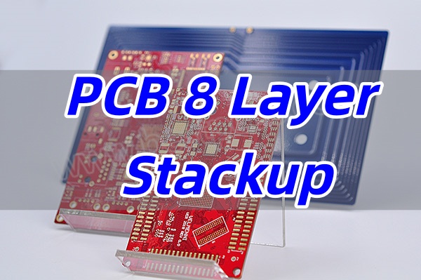
PCB 8 layer stackup is a specific arrangement of copper and insulating layers that provides an optimal balance of performance, density, and signal integrity for complex electronic designs. This article will provide a comprehensive guide to the standard 8 layer PCB stackup, compare it critically with 6-layer alternatives, and explore its key design considerations.
Are you struggling to decide if your high-speed or high-density design truly needs an 8-layer board, or if a 6-layer stackup would suffice?
Performance Anxiety: Worrying that a 6-layer board might not provide sufficient isolation for sensitive signals, leading to crosstalk and electromagnetic interference (EMI).
Routing Congestion: Facing the frustrating reality of not being able to route all the traces on a 6-layer board, especially with complex components like BGAs.
Impedance Mismatch: Struggling to achieve consistent and controlled impedance for high-speed signals, which is more challenging with fewer layers.
Power Integrity Issues: Experiencing noise on the power plane, which can cause erratic circuit behavior and is harder to manage in a 6-layer stackup.
Cost vs. Performance Dilemma: Being caught between the lower cost of a 6-layer board and the superior performance and reliability of an 8-layer PCB, unsure of the right long-term investment.
The good news is that these challenges have clear solutions when you understand the advantages of a well-designed 8 layer pcb stackup and partner with an experienced manufacturer.
Enhanced Signal Integrity: An 8-layer stackup allows for dedicated signal layers adjacent to solid ground planes, effectively minimizing crosstalk and EMI, which directly addresses performance anxiety.
Superior Routing Capability: The two additional layers provide much-needed real estate for routing complex designs, effortlessly solving routing congestion.
Precise Impedance Control: With more layers, achieving a consistent dielectric environment for impedance-controlled traces (like for the 8 layer PCB stackup impedance) becomes more straightforward and reliable.
Stable Power Delivery: Dedicated power planes in an 8-layer stackup offer low-inductance power distribution, ensuring clean power to all components and eliminating power integrity issues.
Optimal Value Proposition: While the initial cost is higher, the enhanced performance, reliability, and reduced need for re-spins often make the 8 layer stackup pcb the more cost-effective solution for advanced applications, resolving the cost vs. performance dilemma.
At BEST Technology, we specialize in manufacturing high-quality, high-performance PCBs. As an original 8 layer PCB factory with 19 years of extensive experience in multilayer boards, we understand the intricacies of PCB 8 layer stackup design. We work with you to determine the optimal stackup, whether it’s a standard 8 layer PCB stackup or a more advanced 8 layer HDI stackup, ensuring your design is built to the highest standards. A warm welcome to contact us at sales@bestpcbs.com to discuss your PCB 8 layer stackup project requirements.
What is the Typical PCB 8 Layer Stackup?
A typical PCB 8 layer stackup is engineered to maximize performance by carefully alternating signal, plane, and dielectric layers. The arrangement is not random; it is designed to shield high-speed signals and provide stable power.
1. Standard Arrangement: A common and effective typical 8-layer pcb stackup follows this sequence from top to bottom: Top Signal -> Ground Plane -> Inner Signal 1 -> Power Plane -> Ground Plane -> Inner Signal 2 -> Power Plane -> Bottom Signal. This “signal-plane-signal” pattern is a cornerstone of good 8 layer pcb stackup design guidelines.
2. Shielding and Isolation: This configuration provides shielding for the inner signal layers (Inner 1 and Inner 2) by placing them between ground planes. This is crucial for reducing noise and crosstalk.
3. Impedance Control: The symmetric structure makes it easier to control the characteristic impedance of traces, which is vital for signal integrity.
In summary, the typical pcb 8 layer stackup is a balanced structure that prioritizes signal integrity, EMI control, and power stability, making it a versatile choice for many demanding applications.
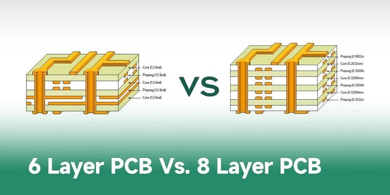
What are the Differences: 8 Layer PCB vs 6 Layer PCB?
The core difference in the “8 layer PCB vs 6” debate lies in the available resources for routing, shielding, and power distribution. The two extra layers in an 8-layer board provide a significant functional advantage.
1. Layer Configuration: A standard 6-layer stackup might be: Signal – Ground – Signal – Signal – Power – Signal. This often forces high-speed signals to be routed on layers adjacent to other signal layers, increasing the risk of crosstalk. In contrast, the PCB 8 layer stackup provides dedicated internal routing layers between ground planes.
2. Performance: The 8-layer board offers superior performance for high-speed designs due to better isolation and the ability to have dedicated power and ground planes. This leads to fewer signal integrity issues.
3. Cost and Complexity: The 6 layer PCB stackup is less expensive and simpler to manufacture. It is an excellent choice for many applications but can become a bottleneck for very high-speed or dense designs.
Ultimately, the choice hinges on the design’s complexity. For applications where signal integrity is paramount, the 8 layer PCB motherboard or similar complex board is the clear winner.
How Thick is an 8 Layer PCB?
The standard thickness of a PCB stackup is often, but not always, around 1.6mm (0.063 inches). However, the final 8 layer PCB thickness is a result of the materials used and the number of layers.
1. Standard and Custom Thickness: While 1.6mm is common, the thickness can vary. The standard 8 layer PCB stackup thickness can be designed to be 0.8mm, 1.0mm, 1.6mm, or even thicker based on the application’s mechanical and electrical requirements.
2. Factors Influencing Thickness: The 8 layer PCB stackup thickness is determined by the thickness of the core and prepreg (insulating) materials, as well as the copper weight. For impedance control, the dielectric thickness between a signal layer and its reference plane is critical.
3. Importance of Specification: When discussing your PCB 8 layer stackup with a manufacturer, it is essential to specify your desired finished thickness and impedance requirements to ensure the stackup is designed correctly.
Therefore, the thickness of an 8-layer PCB is not a fixed value but a key parameter that is carefully engineered during the stackup design phase.
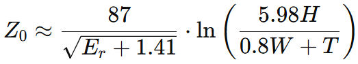
How to Calculate the 8 Layer PCB Stackup Impedance?
Calculating the 8 layer PCB stackup impedance is a critical step for high-speed design, ensuring signals are transmitted without reflection or distortion.
1. Key Parameters: The characteristic impedance of a trace depends on its width (W), the dielectric height (H) to the reference plane, and the dielectric constant (Er) of the insulating material. The copper thickness (T) also has a minor effect.
2. Use of Formulas and Tools: While formulas exist, e.g., for microstrip:
Most engineers use impedance calculation tools provided by manufacturers or integrated into PCB design software like 8 layer PCB stackup altium. These tools automatically calculate the required trace width for a target impedance (e.g., 50Ω or 100Ω differential) based on the defined stackup.
3. Manufacturer Collaboration: It is best practice to finalize your stackup with your PCB manufacturer. They can provide the most accurate Er values and ensure the fabricated board will meet your impedance targets.
Proper impedance calculation is non-negotiable for reliable high-speed performance and is a fundamental part of the 8 layer PCB stackup design guidelines.
How Many Layers can a PCB Have?
PCBs can have a vast number of layers, from 1 to over 50 in extreme cases like advanced servers. The more pertinent question is: do PCB layers matter? The answer is an emphatic yes.
1. Function of Layers: The number of PCB board layers directly determines the board’s functionality. More layers allow for more complex circuitry, better separation of analog and digital sections, improved power integrity, and superior signal integrity through proper referencing and shielding.
2. Choosing the Right Number: A simple electronic device might only need a PCB stackup 4 layer, while a smartphone motherboard might require 10 or 12 layers. The decision for a PCB 8 layer stackup is based on the need for a robust design that can handle multiple high-speed signals and multiple power supplies efficiently.
The number of layers is a fundamental architectural decision that impacts the cost, performance, and reliability of the final product.
What is the 4 Layer PCB Rule?
The “4 layer PCB rule” is a fundamental guideline in PCB design that dictates the optimal arrangement of layers to maximize performance while minimizing cost. It serves as a crucial stepping stone towards understanding more complex stackups like the 8-layer board. While not a rigid law, following this rule is considered a best practice for most 4-layer designs.
1. The Core Principle: Dedicated Plane Layers The most important aspect of the rule is the allocation of the two internal layers. Instead of using them for additional signal routing, they are dedicated exclusively as solid, uninterrupted planes—one for ground (GND) and one for power (PWR). The outer layers (Top and Bottom) are then used for component placement and signal routing.
2. Standard Layer Stackup A typical and effective 4 layer board stackup follows this sequence:
Layer 1 (Top): Components and Signal Routing
Layer 2 (Internal): Ground Plane (GND)
Layer 3 (Internal): Power Plane (PWR)
Layer 4 (Bottom): Components and Signal Routing
3. Key Benefits of This Rule
Improved Signal Integrity: By routing signals on the outer layers adjacent to the solid internal planes, each signal trace has a clear and continuous reference plane. This controlled environment is essential for managing characteristic impedance and significantly reducing electromagnetic interference (EMI) and crosstalk.
Enhanced Power Integrity: The dedicated power plane provides a low-inductance path for distributing power to all components, resulting in a cleaner and more stable voltage supply, which reduces noise.
Superior EMI Performance: The two internal planes act as shields, containing the electromagnetic fields generated by high-speed signals on the outer layers, making the board less susceptible to emitting and receiving interference.
4. Comparison to 2-Layer Boards This rule highlights the major leap in performance from a 2-layer to a PCB stackup 4 layer. A 2-layer board lacks dedicated planes, forcing signals and power to share routing space, which often leads to noise and reliability issues.
In summary, the 4 layer PCB rule is a foundational concept that prioritizes a clean and stable electrical environment. It establishes the core principles of using dedicated power and ground planes, which are then scaled up and refined in more advanced stackups like the 8 layer PCB stackup.
8 Layer PCB Stackup Design Guidelines
Adhering to proven 8 layer PCB stackup design guidelines is fundamental to achieving optimal signal integrity, power integrity, and EMC performance. While the previous section outlined four key principles, a deeper understanding requires grounding these rules in the fundamental goals of all stackup design.
Before delving into specifics, all stackup design aims to satisfy two primary rules:
A Reference Plane for Every Signal Layer: Every high-speed signal routing layer must be adjacent to a solid reference plane (power or ground). This provides a controlled impedance path and a clear, low-inductance return path for signals.
Tight Power-Ground Coupling: Closely spaced power and ground planes are crucial. The minimal spacing between them creates a natural, high-frequency decoupling capacitor that enhances power integrity and reduces EMI.
Understanding the limitations of simpler boards highlights the necessity of a well-designed 8-layer stackup.
Single/Double-Sided Boards: These lack dedicated planes, leading to large signal loop areas which are major sources of EMI and susceptibility. The primary mitigation is to route critical signals (like clocks) with an adjacent ground trace to minimize the loop area.
Four-Layer Boards: While a significant improvement, the standard 1.6mm board thickness creates a large separation between layers, weakening power-ground coupling and making impedance control challenging. The best 4-layer stackup for EMI (GND-SIG/PWR-SIG/PWR-GND) uses outer layers as ground planes for shielding.
Six-Layer Boards: These offer a better balance. A common good stackup is SIG-GND-SIG-PWR-GND-SIG. It provides a reference plane for each signal layer and pairs the power and ground layers. However, achieving tight power-ground coupling within a standard board thickness remains difficult.
An 8-layer board provides the canvas to implement near-ideal stackup design. Here are critical guidelines, moving beyond the basics.
Prioritize Shielding and Symmetry to Prevent Warping The simplest 8-layer stackup (e.g., SIG-SIG-GND-SIG-SIG-PWR-SIG-SIG) is inherently poor. It has multiple consecutive signal layers without reference planes, leading to poor SI and EMI. A superior approach uses symmetry and multiple ground planes. A highly recommended 8 layer stackup is:
Top Signal (Microstrip)
Ground Plane
Internal Signal 1 (Stripline)
Power Plane
Ground Plane
Internal Signal 2 (Stripline)
Power Plane
Bottom Signal (Microstrip) This arrangement is symmetrical, preventing warping. The internal signal layers are shielded between planes, and the ground planes act as excellent EMI shields.
Maximize Interplane Capacitance for Power Integrity Following the core rule of tight coupling, place the power and ground planes that require the best noise immunity (e.g., the core voltage for an FPGA) as adjacent layers (e.g., L4/L5 or L6/L7 in the stackup above). The thin dielectric between them creates a large, low-inductance distributed capacitor that effectively suppresses high-frequency noise on the power rail.
Select the Optimal Stackup for Your EMC and SI Goals The provided material describes three common 8-layer configurations. The best choice depends on your priority:
Good SI, Poor EMI (Example 1): Features many signal layers but lacks sufficient shielding, making it susceptible to radiating.
Good SI, Better EMI (Example 2): This is a strong, common choice. It uses outer ground planes for shielding and has a tightly coupled power-ground plane pair in the center. It offers an excellent balance for most applications.
Best SI and EMI (Example 3): This is the premium configuration, utilizing four ground planes. It provides the highest level of shielding and the cleanest possible return paths for all signals, making it ideal for extremely noise-sensitive or high-radiation applications.
Collaborate with Your Manufacturer Early for Impedance Control This guideline cannot be overstated. Once you have a target stackup, you must work with your PCB manufacturer before finalizing the design. Provide them with your target impedances (e.g., 50Ω single-ended, 100Ω differential). They will feedback the precise dielectric thicknesses and trace widths required to hit your targets based on their specific materials and process capabilities. This is a non-negotiable step in the 8 layer pcb stackup design guidelines.
In summary, designing an 8-layer stackup is an exercise in careful layer ordering to manage return paths, provide shielding, and ensure stable power. By moving from the basic rules to these advanced guidelines—prioritizing shielded stripline layers, tight power-ground coupling, and selecting a stackup based on EMC needs—you can fully leverage the capabilities of an 8-layer board to create a robust, high-performance product.
How is the 8 Layer HDI Stackup?
An 8 layer HDI stackup represents a significant advancement over a standard 8 layer PCB stackup by incorporating High-Density Interconnect (HDI) technologies. It is designed for the most space-constrained and performance-driven applications where miniaturization and complex routing are paramount.
1. Core HDI Technologies HDI stackups are defined by their use of advanced manufacturing processes:
Microvias: These are laser-drilled vias with a much smaller diameter (typically less than 150µm) than mechanically drilled through-hole vias. They allow for connections between adjacent layers (e.g., from Layer 1 to Layer 2) with a minimal footprint.
Finer Traces and Spaces: HDI processes enable the etching of much narrower trace widths and clearances, allowing more circuitry to be packed into a smaller area.
Advanced Build-Up Structures: HDI boards are often built using a sequential lamination process, creating complex sub-composites that can include stacked microvias, staggered vias, and buried vias.
2. Design Advantages over Standard 8-Layer Stackups The integration of HDI technology into an 8 layer stackup PCB offers several critical benefits:
Extreme Miniaturization: By using microvias and finer lines, components can be placed closer together, and the overall board size can be drastically reduced. This is essential for devices like modern smartphones, wearables, and IoT sensors.
Enhanced Signal Performance: Shorter pathways and reduced via stubs from microvias lead to better electrical performance at high frequencies, minimizing signal loss and reflection.
Greater Routing Density: HDI allows for escape routing from high-pin-count components like fine-pitch BGAs, which would be impossible to route on a standard 8 layer PCB motherboard of the same size.
Improved Reliability: The materials and processes used in HDI manufacturing often result in a more robust and reliable board.
3. Typical Applications An 8 layer HDI stackup is not for every project due to its higher cost. It is typically reserved for cutting-edge applications, including:
Smartphones and Tablets
Advanced Medical Implants and Diagnostic Equipment
High-Performance Computing and Networking Hardware
Aerospace and Defense Avionics
In conclusion, the 8 layer HDI stackup is the pinnacle of dense, high-performance PCB design. While a standard typical 8-layer PCB stackup is powerful, the HDI variant pushes the boundaries of what’s possible, enabling the creation of smaller, faster, and more complex electronic devices.
What are the Applications of 8 Layer Stackup PCB?
An 8-layer PCB stackup is widely used in advanced electronic systems where designers need strong signal integrity, stable power delivery, and compact circuit density. These boards support high-speed interfaces, complex processors, and mixed-signal architectures that cannot be achieved with simpler stackups.
Typical applications include:
8-layer PCB motherboards for industrial and embedded computing
High-speed network devices such as routers, switches, and 5G baseband units
Telecommunications infrastructure with dense RF and digital circuits
Automotive electronics including ADAS domain controllers
Medical imaging and diagnostic systems
Industrial automation and rugged control equipment
To show how a real design translates into actual applications, the following example highlights a high-performance 8-layer HDI PCB with engineering features tailored to demanding markets. And the following specific applications are supported by a PCB built to these professional specifications:
Via Type: Resin-filled buried and blind vias
Layer Count: 8-Layer
Material: High-Tg FR-4
Tg Rating: 180°C
Copper Weight: 1oz outer / 1oz inner
Surface Finish: ENIG (1μ″)
Solder Mask: Green
Silkscreen: White
Final Thickness: 1.6mm
Technology: 3-step HDI
1. Core Networking & Communication Systems
Application: Processing and switching board for 100G/200G/400G network equipment.
Why an 8-layer PCB fits: The 3-step HDI structure handles fine-pitch BGA components used in high-bandwidth ASICs and FPGAs. Meanwhile, TG180 FR-4 improves thermal stability during long-term, high-load operation. This combination supports multi-lane SerDes signals and tight impedance control for high-speed communication links.
2. Aerospace and Defense Electronics
Application: Signal processing module for airborne radar or mission-critical avionics.
Why an 8-layer PCB fits: Aircraft electronics experience extreme temperature swings and continuous vibration. 1.6mm finished thickness and TG180 laminate provide strong mechanical strength and thermal endurance. The 1μ″ ENIG finish offers reliable surface quality for gold-wire bonding and high-frequency interconnects common in RF signal chains.
3. Advanced Medical Imaging Equipment
Application: Core electronic module in portable ultrasound or digital imaging diagnostics.
Why an 8-layer PCB fits: Medical devices demand both miniaturization and signal clarity. HDI + resin-filled vias help integrate dense components into a compact format while maintaining stable impedance for sensitive analog/digital imaging circuits. The ENIG surface ensures excellent contact reliability for fine-pitch connectors and probe interfaces.
4. Next-Generation Automotive Electronics
Application: Central computing board for ADAS or autonomous driving systems.
Why an 8-layer PCB fits: ADAS controllers must process multiple high-resolution camera, radar, and LiDAR inputs. An 8-layer stackup provides robust isolation between high-speed differential pairs and noisy power circuits. The 1oz copper thickness supports steady power delivery to high-current SoCs and processing units, ensuring stable performance even at elevated vehicle temperatures.
5. Industrial IoT and Edge Computing Devices
Application: Industrial edge gateway, PLC controller, or machine-vision interface.
Why an 8-layer PCB fits: Factories require devices that remain stable under dust, humidity, vibration, and electrical noise. The ENIG finish prevents oxidation, and the green solder mask + white silkscreen combination improves maintenance visibility. The rigid 8-layer architecture enhances long-term reliability for 24/7 operation in challenging industrial environments.
In closing, this example makes it clear that an 8-layer PCB stackup is far more than a simple increase in layer count. With the right combination of materials, HDI structures, and controlled-impedance routing, it becomes a powerful platform for mission-critical, high-speed, and high-density electronic systems across multiple industries.
In conclusion, PCB 8 layer stackup is a sophisticated multilayer board configuration that offers a significant performance upgrade over 6-layer alternatives for demanding electronic applications. This article has explored the structure, advantages, and design considerations that make the 8-layer stackup a preferred choice for high-speed and high-density designs.
For engineers seeking reliable, high-performance PCB 8 layer stackup fabrication, partnering with an experienced 8 layer PCB manufacturer is crucial. At BEST Technology, we have the expertise to guide you through the entire process, from selecting the best 8 layer stackup for your needs to ensuring impeccable manufacturing quality. Pls feel free to contact us at sales@bestpcbs.com to get started on your next 8 layer stackup PCB project.
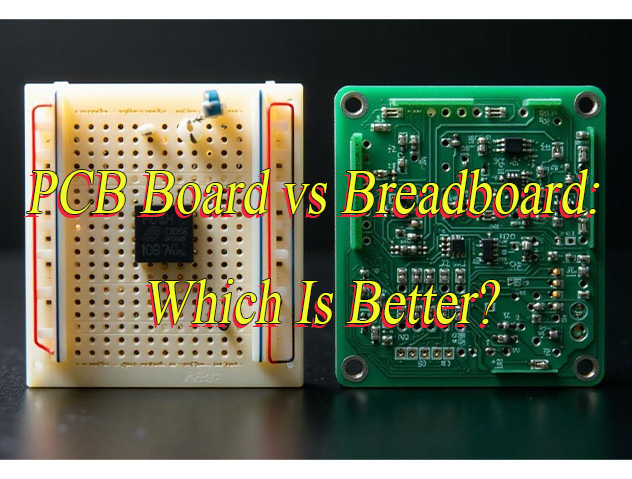
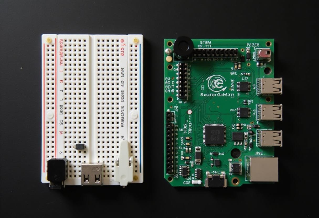
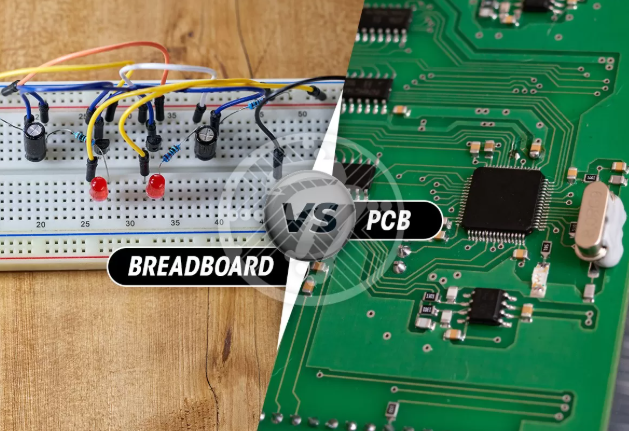
PCB board vs breadboard: which is better? This blog mainly covers cost and application difference, selection guide for PCB board and breadboard.
Are you troubled with these issues?
Breadboard contacts are prone to cold solder joints, resulting in poor signal stability. How can reliable circuit performance be ensured?
High-frequency signals are easily interfered with on breadboards, leading to long debugging cycles. How can verification time be shortened?
Loose breadboard layouts are difficult to adapt to compact product spaces. How can a seamless transition from prototype to mass production be achieved?
As a professional PCB board manufacturer, EBest Circuit (Best Technology) can provide you service and solutions:
Precision PCB Prototyping Service: Eliminating the risk of cold solder joints and ensuring stable signal transmission through micron-level circuit etching and pad optimization.
Electrical Characteristic Verification Support: Providing multilayer board impedance control and ground plane copper pour design to reduce high-frequency signal crosstalk and improve debugging efficiency.
Mass Production Design Guidance: Intervening from the prototype design stage to optimize layout, routing, and manufacturability (DFM) to ensure a smooth transition from small-batch production to mass production.
A breadboard is a solderless experimental board used for quickly building and testing circuit prototypes. It typically consists of a plastic board with many small holes, connected internally by metal strips. This allows the pins of electronic components to be inserted into the holes and connected via wires to build the circuit. Its main advantages are that it requires no soldering, is reusable, and makes circuit building and modification very convenient, making it ideal for functional verification and debugging in the early stages of circuit design. However, its contact connections have relatively poor stability, making it unsuitable for high-frequency circuits or long-term use.
What Is A PCB Board?
A PCB, or Printed Circuit Board, is the final circuit carrier of electronic products. It is created by printing wires, lines, and holes onto a substrate using electronic processes. Electronic components are then soldered onto the board to achieve complex and stable circuit functions, used in the mass production of various electronic devices. The advantages of PCBs include high connection reliability, strong anti-interference capabilities, and suitability for large-scale production and long-term stable use. However, their design and manufacturing cycles are relatively long, prototyping costs are high when not in mass production, and modifications are very difficult once completed.
Breadboard: ideal for rapid prototyping, educational experiments, early-stage research, and creative electronics projects (e.g., Arduino/STM32 development, sensor testing, basic circuit experiments). Its plug-and-play nature eliminates soldering, supports component reuse, and suits temporary or small-scale projects, especially for beginners and educational settings.
PCB board: excels in mass production, complex circuits, high-frequency circuits, and high-reliability scenarios (e.g., medical devices, industrial control, automotive electronics, aerospace, IoT devices). Soldering provides stable electrical connections, enables high-density integration, and meets long-term stability demands.
Cost and Benefit Analysis
Breadboard: has a low initial cost (single board costs tens of dollars), suitable for low-budget or short-term projects. However, frequent plugging/unplugging may cause poor contact, increasing long-term maintenance costs, and is unsuitable for high-frequency/complex circuits.
PCB board: has a higher initial cost (design, fabrication, and processing fees) but unit costs drop significantly with mass production. Its high reliability and low failure rate reduce overall costs in the long run, especially for mass production and precision equipment.
Design and Flexibility Comparison
Breadboard: offers design flexibility, allowing instant component replacement and supporting rapid iteration. However, messy wiring, low integration density, and difficulty in high-density/high-frequency circuit design are drawbacks.
PCB board: requires professional software (e.g., Altium, Eagle) for design, supports precise layout and high-density integration, and suits complex circuits and customization. Once fabricated, circuits are fixed, requiring re-fabrication for modifications, but enables anti-interference and high-precision designs.
Reliability and Stability
Breadboard: Physical contact connections are susceptible to mechanical stress, leading to poor contact or signal interference, especially in high-frequency or precision circuits.
PCB Board: Solder joints provide stable electrical connections, strong anti-interference capabilities, and meet industrial-grade reliability standards (such as ISO certification), making it suitable for high-precision, high-reliability applications (such as medical equipment and aerospace).
Maintenance and Scalability
Breadboard: allows easy maintenance with replaceable components but frequent plugging may accelerate aging. Scalability is limited; large-scale circuits require multiple boards connected with wires, leading to messy wiring.
PCB board: requires professional tools for maintenance but has low failure rates. It supports modular design and batch soldering, offers strong scalability, and enables functional upgrades via layer addition or layout optimization, suitable for long-term use and mass production
Environmental Protection and Compliance
Breadboard: materials are recyclable, but frequent replacements may generate waste.
PCB board: uses lead-free soldering and eco-friendly materials (e.g., FR-4), complying with international environmental standards (e.g., RoHS), suitable for exports to regions with strict environmental requirements (e.g., Europe, US).
Low-complexity/low-frequency circuits (e.g., LED arrays, simple sensors, basic logic circuits): Breadboard suffices due to fewer contact points, lower costs, and minimal parasitic parameter impact on low-frequency signals.
High-complexity/high-frequency/precision circuits (e.g., RF modules, high-speed digital circuits, precision analog circuits): PCB is essential. High-frequency signals are sensitive to parasitic capacitance/inductance; PCB enables signal integrity optimization via multi-layer routing, ground plane design, differential pairing, and noise/crosstalk/attenuation mitigation.
3. Balance Cost & Time Efficiency
Short-term cost sensitivity: Breadboard has low initial investment (5−50), suitable for budget-constrained or short-cycle projects (e.g., temporary demos, student projects). However, long-term use may incur hidden maintenance costs due to contact oxidation/loosening.
Long-term cost optimization: PCB design/fabrication fees are higher upfront, but per-unit costs drop significantly in bulk (e.g., <$5/unit at 1,000+ pieces). Supports SMT automation, ideal for stable long-term demand or scaled production.
Frequent modifications/modular design: Breadboard supports plug-in component adjustments, ideal for algorithm validation or multi-version testing. However, prolonged use may cause contact wear and faults.
Fixed design/mass production: PCB designs are static; modifications require costly re-fabrication. However, integrated test points and identifiers streamline batch production quality control and troubleshooting, suitable for standardized product development.
6. Align with Technical Maturity & Team Expertise
Beginners/non-professional teams: Breadboard lowers entry barriers, requiring no soldering skills, ideal for hobbyists, students, or small teams.
Professional engineers/enterprise R&D: PCB design demands professional tools (e.g., Eagle, Altium Designer) and fabrication processes, suitable for experienced teams or projects requiring high precision/reliability.
Prioritize Breadboard: When projects are in early exploration, require rapid concept validation, have limited budgets, or low reliability demands.
Prioritize PCB: When projects demand productization, mass production, strict signal quality/anti-interference requirements, or involve high-frequency/precision circuits.
Transition Strategy: Validate logic/functionality on Breadboard first, then transition to PCB once design stabilizes—this balances development efficiency with product quality, a common practice among global engineers, makers, and R&D teams.
When to Use Breadboard Instead of PCB Board?
Rapid Prototyping and Proof-of-Concept: Breadboards are the preferred choice when you need to quickly build electronic circuit prototypes to validate your design ideas. They require no soldering, support rapid plug-and-play and circuit modifications, making them suitable for rapid design iteration in the early stages of development. For example, makers and startups abroad often use breadboards to quickly test the compatibility of components such as sensors and microcontrollers, saving time and costs associated with PCB design and production (which typically takes days to weeks).
Education and Learning Scenarios: For students, educational institutions, and DIY enthusiasts, breadboards are used as teaching tools due to their intuitive and easy-to-use features. For example, in electronics courses in primary and secondary schools abroad, students can intuitively understand circuit connection principles (such as series/parallel connections) using breadboards without needing to learn complex PCB design software or soldering processes, lowering the learning threshold.
Temporary Testing and Troubleshooting: In the later stages of product development or in repair scenarios, breadboards can quickly build test circuits to locate problems. For example, when engineers need to verify the functionality of a module, they can temporarily build test circuits using breadboards, avoiding the high costs of repeatedly modifying PCB designs (the cost of a single PCB fabrication can reach hundreds of dollars).
Low-complexity, short-term use projects: For one-off, short-term projects (such as exhibition demonstrations and temporary exhibits), breadboards are more advantageous due to their low cost and reusability. International clients often choose breadboards to build simple demonstration circuits, avoiding the high costs of PCB fabrication for short-term needs.
Design flexibility requirements: When designs require frequent adjustments or exploration of multiple solutions, the modular nature of breadboards allows users to disassemble and reassemble circuits at any time. For example, international R&D teams may use breadboards in the early stages of development to quickly try different combinations of resistors and capacitors to optimize circuit performance without having to create multiple PCB prototypes.
How Does Cost Difference between PCB Board and Breadboard?
Breadboard: $0.50–$8.00+. Basic models (400-830 holes) typically range from $2.00 to $5.00. Larger quality models or those with accessories (power rails, bases) can reach $8.00+.
PCB (Single/Small Batch Prototype): $2.00–$50.00+. Costs are greatly affected by size, number of layers, complexity, materials, processes, and lead time. The sample price (e.g., 5 pieces) of the most basic double-layer board (~10cm x 10cm, FR-4, standard parameters) spreads to approximately $5.00–$15.00 per piece. More complex boards (multi-layer, high-density, special materials/processes) or rush orders easily exceed $20.00–$50.00+ per piece.
How to Choose A Reliable Breadboard Manufacturer?
1. Hard Qualification Verification
International Certifications & Standards: Prioritize manufacturers with ISO 9001:2015 (Quality Management), ISO 14001 (Environmental Management), UL/CE (Safety Certifications) to comply with target markets like EU/US regulations. Verify certificate authenticity and validity via official certification agency websites.
Raw Material Traceability & Quality Control: Request supplier lists for raw materials (e.g., ABS plastic, copper foil) and confirm compliance with RoHS/REACH. Inspect quality control points (e.g., soldering temperature, board flatness) through on-site audits or third-party testing.
2. Production Capacity Assessment
Capacity & Customization: Evaluate monthly output (e.g., 10,000+ pieces/month) and confirm support for small-batch trials (e.g., <500 pieces) and rapid prototyping (3-5 days). Check customization options (dimensions, colors, logo printing) and mold development capabilities.
Technology & R&D: Review R&D investment ratios and patent portfolios (e.g., conductive materials, anti-oxidation coatings). Prefer collaborations with universities/research institutions for technical leadership.
3. Client Case & Reputation Verification
Industry Case Studies: Request overseas client cases from the past 3 years (e.g., EU electronics firms, educational institutions), focusing on product/order scale alignment and regional market match.
Third-Party Reviews: Source feedback from trade fairs, B2B platforms (Alibaba), or review sites (Trustpilot) for metrics like on-time delivery and after-sales response. Avoid relying solely on curated testimonials.
4. Communication & Service Quality
Cross-Cultural Communication: Confirm multilingual (English/Spanish) sales teams and 24/7 support. Test response times (<12 hours) and issue resolution (e.g., sample defect handling).
After-Sales System: Clarify warranty periods (1-3 years), return policies, and tech support methods (video tutorials, remote assistance). Overseas clients prioritize local services (e.g., EU warehouses, regional repair centers).
5. Logistics & Supply Chain Transparency
Export Experience & Logistics Network: Select manufacturers with 5+ years of export experience and familiarity with trade terms (FOB/CIF). Evaluate logistics partners (DHL/FedEx) and storage networks (EU overseas warehouses) for controlled lead times (3-7 days air, 30-45 days sea).
Supply Chain Visibility: Demand traceability data (material batches, production dates) and third-party logistics tracking (bill of lading numbers, shipment tracking).
Welcome to contact us if you have any request for breadboard or PCB board: sales@bestpcbs.com.
How to design a castellated PCB? This blog is mainly about design guideline and considerations, production process for castellated PCB.
Are you troubled these issues with castellated PCB?
Is board space extremely limited while traditional connections occupy too much area and fail reliability?
When welding modules to mainboards, is alignment often imprecise, causing high yield fluctuations and production costs?
Want compact board-to-board assembly but face complex processes, long cycles, and struggle to match product iteration speeds?
As a castellated PCB manufacturer, EBest Circuit (Best Technology) can provide you service and solutions:
Process Guarantee: Specializing in castellated PCB precision machining, we use unique processes and full-cycle quality control to ensure full copper plating, smooth hole walls, and stable “golden fingers” for reliable board connections.
Design Collaboration Optimization: Professional front-end DFM analysis services identify design-phase risks early, optimizing module layouts and castellated structures for precise alignment and efficient assembly.
Efficient Flexible Production: Rapid-response production lines for small/medium batches reduce lead times, flexibly align with R&D rhythms and market demands, and accelerate market entry.
Feel free to contact us if you have inquiry for castellated PCB: sales@bestpcbs.com.
What Is a Castellated Hole PCB?
A Castellan Hole PCB is a type of printed circuit board with specially designed semi-circular gold-plated holes (resembling castle crenellations) machined along its edges. Its core feature is that these holes are precisely cut into half-holes along the board edge, and the hole walls are metallized, exposing the internal conductor layers. This design allows the PCB to be soldered directly to the pads of another PCB through the metallized layer on the half-hole, just like surface mount technology (SMT) components, achieving a reliable vertical interconnection between boards.
Why Use Castellated Holes in PCB?
Achieving Vertical Board-to-Board Interconnection: Core Advantages. Allows one PCB to be directly and vertically soldered to the pads of another PCB via a metallized layer on a half-hole, just like a surface mount device (SMT) component, creating a compact 3D structure.
Significant Space Savings: Vertical stacking greatly optimizes the utilization of internal space, especially suitable for space-constrained miniaturized and portable electronic products.
Simplified Assembly Process: Eliminates the need for additional connectors such as sockets, pin headers, cables, or flexible printed circuit boards (FPCs) required for traditional board-to-board connections, reducing material costs and assembly steps.
Improved Connection Reliability: Direct SMT solder joints are formed between the metallized half-holes and the pads, providing stronger mechanical strength and electrical contact reliability than plug-in connectors, and offering better vibration resistance.
Reduced Overall Cost: By eliminating external connectors and their assembly costs, and simplifying the production process (compatible with standard SMT processes), the bill of materials (BOM) and manufacturing costs of the product can be effectively reduced.
Enhanced Design Flexibility: Facilitates modular design. Functional modules (such as Wi-Fi/BT modules and power modules) can be prefabricated as independent daughterboards with castle holes, simplifying the main system design and facilitating replacement and upgrades.
How To Design A Castellated PCB?
1. Define Design Goals and Constraints
Functional Requirement Definition: Engage in in-depth communication with clients to clarify electrical performance (e.g., signal speed, impedance requirements), mechanical dimension constraints (e.g., castellation pitch, height), thermal management needs (e.g., heat dissipation path, power dissipation), and environmental adaptability (e.g., temperature range, vibration resistance).
Standards and Specification Compliance: Adhere to international standards (e.g., IPC-2221A, IPC-4761) and client-specific specifications, including EU RoHS/REACH environmental requirements and UL safety certifications.
Layer Stack Planning: Design stack-up based on signal integrity needs. For high-speed digital circuits, use 6-layer structures (signal-ground-power-signal-ground-signal) to ensure impedance continuity (e.g., 50Ω single-ended, 100Ω differential).
Material Selection: Choose high-frequency/high-speed substrates (e.g., Rogers 4350B, Isola I-Tera MT40) to reduce dielectric loss, or high-Tg materials (Tg ≥170°C) for thermal stress resistance. Copper thickness matches current capacity (e.g., 1oz for signal layers, 2oz for power layers).
Ground Plane Design: Implement continuous ground planes covering critical signal areas to minimize signal return paths. Use thin dielectrics (e.g., 50μm) between power and ground planes to reduce PDN impedance.
3. Layout and Routing Strategies
Layout Principles: Partition functional modules (digital, analog, power zones). Place sensitive components (e.g., crystal oscillators) away from heat sources and noise sources. Avoid precision components near castellation edges to prevent mechanical stress damage.
Routing Rules: Route high-speed signals as differential pairs (length matching ±5mil, spacing ≥3× line width). Avoid 90° turns (use 45° or curved paths). Calculate power trace width for current capacity (e.g., 10mil width for 1A current) and use multiple vias for parallel resistance reduction.
Castellation Edge Handling: Add non-functional pads (e.g., 1mm×1mm) at sawtooth edges for mechanical reinforcement. Chamfer edges (e.g., R0.5mm) to reduce stress concentration.
4. Thermal Design and Heat Management
Heat Dissipation Path Planning: Place high-power devices (e.g., power MOSFETs) over thick copper pours (≥2oz) and connect to ground planes via thermal vias filled with solder paste. Design castellation edges as heat sinks to increase air contact area.
Thermal Via Design: Deploy dense thermal vias (e.g., 0.3mm diameter, 1mm spacing) under heat sources to form thermal channels. Fill vias with conductive materials (e.g., copper paste) to enhance thermal conductivity.
Simulation Validation: Use thermal simulation tools (e.g., ANSYS Icepak) to verify temperature distribution, ensuring peak temperatures stay below component limits (e.g., junction temperature ≤125°C).
5. Signal Integrity and EMC
Impedance Control: Calculate stack-up parameters to ensure critical signal line impedance matching (e.g., using Polar SI9000). Apply back-drilling to minimize stub effects.
Crosstalk Mitigation: Increase shielding for sensitive signals (e.g., 3W rule) or use ground shielding. Maintain sufficient spacing between high-speed differential pairs (≥3× line width).
EMC Design: Add π-type filters (inductor + capacitor) at power entry points. Place decoupling capacitors (e.g., 0.1μF + 10μF) near critical ICs. Avoid antenna effects at castellation edges (e.g., long traces).
6. Testability and Reliability
Test Point Design: Place test pads (≥1mm diameter) at critical nodes (power, signal I/O) with labeled identifiers. Boundary scan (JTAG) interfaces must comply with IEEE 1149.1.
Mechanical Reliability: Validate vibration resistance via stress analysis (e.g., ANSYS Mechanical). Reinforce critical connector areas with stiffeners (e.g., L-shaped copper traces).
DFM Checks: Perform DRC/ERC checks using EDA tools (e.g., Altium Designer, Cadence Allegro) to ensure compliance with manufacturing tolerances (e.g., minimum trace/spacing ≥4mil). Generate Gerber files and drilling data.
7. Testability and Reliability
Design Documentation: Compile detailed specifications (BOM, stack-up, routing rules), assembly drawings, and test procedures. Provide 3D models (e.g., STEP format) for mechanical fit evaluation.
Version Control: Track design changes using version control systems (e.g., Git) for traceability. Final deliverables include Gerber files, BOM, coordinate files, and process notes.
Castellation PCB Design Technical Parameter
Parameter Name
Recommended Value/Range
Drill Diameter
0.4 mm – 1.0 mm
Pad Diameter
Drill Diameter + 0.2 mm
Depth
Board Thickness
Pitch
≥ 0.5 mm (High-density designs may reduce to 0.4 mm with DFM evaluation)
Edge Clearance
≥ 0.3 mm
Cu Plating Thickness
Minimum 20 μm (0.8 mil)
Surface Finish
ENIG / HASL / Immersion Tin
Hole Wall Roughness
≤ 35 μm
Burr Control
No visible burrs
Solder Mask Opening
Single-side expansion 0.05-0.1 mm
Thermal Shock Test
-40°C to +125°C
Solderability
Wetting area ≥95%
PCB Castellated Edges Design Consideration
Mechanical Strength and Dimensional Design
Minimum Hole Diameter Requirements: PCB half-hole diameter must be determined based on board thickness. For boards under 1.0mm thick, a minimum half-hole diameter of 0.6mm is recommended; for boards over 1.6mm thick, a minimum half-hole diameter of 1.0mm is advised.
Edge Spacing: Maintain a minimum distance of 10–15% of board thickness between half-hole edges and outer copper foil edges to minimize stress concentration and ensure soldering quality.
Pattern Consistency and Alignment: Precise alignment between pads and drilled holes is critical. Include adequate fiducial marks to reduce component misalignment risks.
Electrical Signal Integrity
Reference Layer Management: Avoid cutting through power and ground planes near half-holes. Implement reference layer bridging (keep-out area bridge design) to mitigate impedance mismatches.
Shielding Design: For RF/high-frequency applications, incorporate metallized shielding edges and alternating pad layouts to reduce EMI.
Coaxial Signal Path Recommendations: When routing high-speed differential lines, maintain consistent spacing along pads. For high-density communication modules, perform impedance simulation to validate design parameters.
Process Standardization
Pad Geometry Design: Half-hole pads should be oval-shaped or extended to the edge to ensure adequate plating coverage (≥65% metal retention post-drilling).
Pre-Soldering Preparation: Apply epoxy hole fill or solder mask control in half-hole soldering zones to enhance SMT reliability.
Plating and Surface Coating: Use ENIG (Electroless Nickel Immersion Gold) or immersion tin for full-board plating. Employ step plating to ensure uniform metallization in half-hole walls.
Manufacturing Compatibility
Process Time and Cost: Many international PCB fabricators require high-precision milling tools for panelized half-hole cutting. Confirm equipment capabilities support continuous half-hole slot cutting dimensions.
Thermal Stress Optimization: Integrate thermal relief designs aligned with end-device thermal cycling profiles to prevent soldering failures from thermal cycling.
Testing and After-Sales Support
ICT Interface Design: Include test points in the layout to accommodate FCT (Functional Circuit Test) tooling customization.
Documentation Clarity: Clearly annotate half-hole positions in assembly diagrams to prevent reflow misalignment.
Failure Diagnostics Support: Document common failure modes (e.g., insufficient solder, terminal lifting) with inspection guidelines and troubleshooting steps.
How to Make A Castellated PCB?
1. Substrate Preparation and Lamination
Material Selection: Choose FR-4, high-frequency materials, or flexible substrates, coated with electrolytic copper foil (thickness ≥35μm) to ensure conductivity and mechanical strength.
Lamination Process: Bond inner core boards, prepregs (PP), and outer copper foils through high temperature and pressure to form a multi-layer structure, controlling interlayer alignment accuracy to ±0.05mm.
2. Drilling and Plating
Full Hole Drilling: Drill complete through-holes (diameter 0.6-1.2mm) at the board edge using tungsten carbide drills or laser drilling (for HDI boards with hole diameters ≤0.1mm).
Hole Metallization: Apply chemical copper deposition (0.3-1μm) to cover the hole walls, followed by electroplating to thicken the copper layer to 25-30μm, ensuring electrical connectivity. Use pulse plating or electroless copper plating to avoid copper layer tearing.
3. Outer Layer Circuit Formation
Photolithography and Etching: Apply film, exposure, and development to form etch-resistant patterns, then etch away unprotected copper to retain circuits and copper in the half-hole area. After stripping the film, perform secondary copper/tin plating for protection.
Solder Mask and Silkscreen: Spray liquid photoimageable solder mask, UV cure to form the solder mask layer (with precise openings), and silkscreen identification information to prevent solder bridging.
4. Half-Hole Shaping
Cutting Process: Use precision milling cutters (double-V shaped tool path) or laser cutting along the hole center to retain the half-hole structure. Optimize spindle speed and feed rate with slot cutters to reduce burrs and copper lifting.
Deburring: After cutting, use alkaline etching or red tape to bond unit boards and remove residual copper filaments, ensuring smooth, defect-free half-hole edges.
5. Surface Finish
Enhanced Solderability: Apply ENIG, OSP, or immersion tin to improve pad solderability and oxidation resistance. For high-frequency applications, use immersion silver or gold plating.
Solder Mask Bridge Design: Set a solder mask bridge of ≥0.1mm between half-holes to prevent solder short circuits. Use NSMD design in non-solder mask areas to enhance solder joint reliability.
6. Profiling and Testing
Outline Cutting: Use CNC milling or V-cut to cut the final outline, ensuring dimensional accuracy.
Electrical Testing: Perform flying probe or ICT testing for continuity and insulation resistance. Use AOI/AXI to inspect pad alignment and inner layer defects.
Reliability Verification: Conduct high-temperature aging, thermal shock, and vibration tests to verify mechanical strength and electrical performance (e.g., IPC Class 3 standards).
7. Quality Control and DFM Optimization
Precision Control: Monitor dimensional deviations in drilling, lamination, and cutting to avoid inconsistent half-hole sizes due to swelling or shrinkage.
DFM Guidelines: Follow manufacturer guidelines (e.g., minimum hole diameter 0.5mm, edge gap 0.5mm) and optimize designs to reduce manufacturing difficulty and costs.
Why Choose EBest Circuit (Best Technology) as Castellated PCB Manufacturer?
Free DFM Analysis: Professional team provides free Design for Manufacturability (DFM) analysis to identify potential manufacturing defects at the design stage, reducing trial production costs and time by over 30% for a one-time successful design.
End-to-End One-Stop Service: Comprehensive services from design optimization and rapid prototyping to mass production delivery. Single point of contact handles all processes, boosting efficiency by 40% and ensuring smooth project progression.
1 Piece MOQ: Supports small-batch and single-piece orders to meet prototype validation and small-scale trial production needs, lowering initial investment risks and enabling rapid design iteration to capture market opportunities.
19 Years of Technical Expertise: Deep experience in PCB manufacturing with over 5,000 complex projects completed. Specializes in high-density interconnect (HDI) and miniaturized designs to ensure flawless execution of innovative concepts.
Globally Recognized Quality Certifications: Holds ISO 13485 (medical), AS9100D (aerospace), and IATF 16949 (automotive) certifications, meeting stringent requirements for high-reliability applications in medical, aerospace, and automotive sectors.
Custom Material Solutions: Offers tailored material options including ultra-thin substrates, high-frequency high-speed materials, and high-temperature specialty materials to match diverse application scenarios from consumer electronics to industrial controls.
Engineer-Centric Support: Bilingual technical team provides 24/7 support, covering design specification interpretation and production issue diagnosis to reduce communication costs and ensure project success.
Eco-Friendly Manufacturing Commitment: Utilizes lead-free processes and wastewater recycling systems compliant with RoHS/REACH standards, facilitating seamless international environmental certification and enhancing global market access.
Welcome to contact us if you have any request for castellated PCB: sales@bestpcbs.com.
Best PCB manufacturers in China represent a group of leading electronics manufacturing service (EMS) providers renowned for combining advanced technological capabilities with cost-effectiveness. This comprehensive guide will explore the key players, selection criteria, and technical strengths that define the top-tier PCB supply chain in China, with a specific focus on full-turnkey services from design to box build.
Are you struggling to navigate the vast landscape of PCB production in China, worried about quality consistency, communication barriers, or finding a partner that can handle complex projects like HDI PCBs from design to box build?
Uncertain Quality: Fear of receiving substandard boards that fail in testing or have a short lifespan.
Communication Challenges: Time zone differences and language barriers leading to misunderstandings and project delays.
Limited Technical Scope: Finding a manufacturer that only does fabrication, forcing you to manage assembly separately.
Inconsistent Pricing: Hidden costs and fluctuating quotes that blow the project budget.
Long Lead Times: Slow production and shipping timelines that impact your product’s time-to-market.
The good news is that these common challenges have clear solutions when you partner with best PCB manufacturers in China.
Stringent Quality Control: Implementation of rigorous quality management systems (like ISO 9001, IATF 16949) and multiple inspection points throughout production.
Dedicated Customer Support: Assigning experienced project managers who provide clear, proactive communication in English.
Full Turnkey Services: Offering an integrated solution that includes PCB fabrication, component sourcing, PCB assembly, and final box-build assembly.
Transparent Quoting: Providing detailed, upfront quotes with no hidden fees, often with cost-saving design for manufacturability (DFM) advice.
Optimized Production Flow: Utilizing advanced equipment and streamlined processes to guarantee fast PCB manufacturing without sacrificing quality.
Among the PCB manufacturers in China, BEST Technology stands out as a premier partner. We are a professional PCB and EMS factory with over 19 years of experience, specializing in providing end-to-end solutions from design and prototyping to mass production and box-build assembly. Our commitment to quality, advanced technical capabilities in areas like HDI PCB, high speed board, RF printed circuit board, copper MCPCB, star MCPCB, ceramic base PCB, and exceptional customer service make us a trusted choice for global clients. For inquiries, pls feel free to contact us at sales@bestpcbs.com.
What Factors Define the Best PCB Manufacturers in China?
Selecting the right partner goes beyond just comparing prices. The best PCB manufacturers in China are distinguished by a combination of capabilities, certifications, and services that ensure reliability and value.
Comprehensive Service Range: The top manufacturers offer a complete “Design to Box Build” service. This includes PCB layout support, PCB fabrication, component procurement, PCB manufacturing and assembly, testing, and final product integration. This simplifies the supply chain and ensures accountability at every stage.
Technical Proficiency and Specialization: Look for manufacturers with expertise in the specific technologies you need. This includes capabilities for standard boards, as well as advanced processes for HDI PCB, high-frequency boards, heavy copper, and flexible circuits. Their technical depth directly impacts your product’s performance.
Robust Quality Assurance Systems: Certifications like ISO 9001, ISO 13485, IATF 16949, AS9100D are baseline indicators. The best manufacturers have in-house testing labs (for ICT, Flying Probe, X-Ray, etc.) and a proven track record of high yield rates.
Transparent Communication and Project Management: Effective communication is critical. The leading providers assign a dedicated project manager to act as a single point of contact, providing regular updates and swiftly addressing any concerns.
Proven Experience and Reputation: A long history of successful projects, especially with international clients, is a strong positive signal. Client testimonials and case studies offer valuable insights into their reliability and performance.
In summary, the best manufacturers are those that provide a seamless, high-quality, and transparent partnership, mitigating the risks typically associated with overseas production.
Is BEST Technology a PCB Manufacturer in China?
Yes, absolutely. BEST Technology is a established and well-regarded PCB manufacturer in China.
We operate our own modern manufacturing facilities equipped for both standard and advanced PCB fabrication.
Our services extend far beyond simple board production; we are a full-scale EMS provider.
This means we manage the entire process, from sourcing raw materials and components to PCB manufacturing and assembly, and finally, assembling the finished product into its enclosure (box build).
Our integrated approach ensures greater control over quality, cost, and scheduling, making us a true one-stop-shop for our clients.
Top 10 Best PCB Manufacturers in China
While rankings can vary, the following list represents some of the most prominent and capable PCB manufacturers in China, known for their scale, quality, and service offerings. This China PCB manufacturer list includes:
BEST Technology: Distinguished by our strong focus on engineering support and full turnkey PCB manufacturing and assembly services, especially for complex projects requiring HDI PCB, PCBA and reliable box-build assembly.
PCBWay: A major player in the prototype and small-batch market, offering a wide range of capabilities and an active online community.
Kingboard Holdings: One of the largest PCB manufacturer in the world, supplying a massive volume of boards to various industries.
Shennan Circuits Co., Ltd. (SCC): A leading manufacturer focusing on high-end, high-layer count boards for communications and servers.
AT&S: A global high-end PCB supplier with significant production bases in China, specializing in HDI and substrate-like PCBs.
WUS Printed Circuit Co., Ltd.: A major manufacturer with strong capabilities in automotive and communication PCBs.
Kinwong Electronic: A large-scale producer with a strong presence in automotive, consumer electronics, and data storage.
JLC PCB (Shenzhen JLC Electronics Co., Ltd.): Best known for its incredibly user-friendly online platform and low-cost, quick-turn prototypes.
Tripod Technology Corporation: A top-tier global manufacturer with extensive facilities in China, producing a wide range of PCB types.
Compeq Manufacturing Co., Ltd.: A major supplier of HDI, flexible, and rigid-flex PCBs for smartphones and consumer devices.
This top 10 PCB manufacturers in china list showcases the diversity of the market, from giants focused on volume to specialized partners like BEST Technology that excel in comprehensive service.
How to Choose Between Top PCB Manufacturers in China and the Best PCB Manufacturers in USA?
The choice between a Chinese and a US-based manufacturer involves a trade-off between several key factors.
Cost: This is the most significant advantage for Chinese manufacturers. Lower labor and overhead costs typically result in substantially lower prices, especially for medium to high-volume production.
Lead Time and Logistics: Best PCB manufacturers in USA offer shorter shipping times and can be advantageous for rapid iterations or projects with very tight timelines. However, many Chinese manufacturers have optimized their processes for Fast PCB manufacturing and offer expedited shipping options.
Communication and IP Protection: US-based manufacturers have no language barrier and operate under US intellectual property laws, which some companies prefer. Reputable Chinese manufacturers like BEST Technology have English-speaking teams and strict NDAs to protect client IP.
Technical Capability: Both regions have highly capable manufacturers. China’s ecosystem is vast, with many specialists in advanced technologies like HDI PCB. The choice often comes down to the specific technical requirements of the project.
Overall, for projects where cost-efficiency is paramount and volumes are medium to high, the best PCB manufacturers in China are typically the superior choice, especially when you partner with a reliable provider that mitigates concerns about communication and quality.
What are the Technical Capabilities of the Manufacturer of HDI PCB in China?
When you work with the manufacturer of HDI PCB in China, such as BEST Technology, you are essentially partnering with a factory built around high-density, high-precision interconnect technology—not just standard multilayer boards. Our capabilities cover the full chain from via structure design to complex stack-ups, materials, and final finishing.
Below is a consolidated view of our main technical strengths, based on real HDI manufacturing capabilities at BEST Technology.
1. Full Range of HDI Via Structures
We design and manufacture all the core via types used in HDI PCB:
Blind vias – connecting outer layers to one or more inner layers without passing through the whole board.
Buried vias – connecting only internal layers, invisible from outside.
Through-hole vias – standard plated through holes for robust interconnection and mechanical support.
For HDI, we distinguish clearly between:
Laser microvias (HDI vias)
Laser-drilled diameter down to 0.07mm (70µm) for prototypes.
Standard production microvia diameter around 0.10mm.
Dielectric-to-hole aspect ratio controlled at about 1:1 to maintain plating stability.
Use of RCC or laser-drillable prepregs for consistent microvia quality.
Mechanical blind/buried vias
Hole diameters typically ≥0.20mm.
A cost-effective choice when extreme density is not required.
2. Advanced Laser Drilling and Microvia Technology
We use advanced UV and CO₂ laser systems optimized for different copper thicknesses and dielectric stacks.
Arlon (Suitable for RF, 5G, high-speed digital, impedance-controlled systems)
Thin-core HDI capability
Minimum inner core thickness 0.05mm
Enables compact, multi-stack HDI structures
This material flexibility allows us to optimize stack-ups for signal integrity, thermal performance, and cost.
6. Surface Finishes Optimized for HDI and Fine Pitch
We offer a full portfolio of finishes for fine-pitch and wire-bonding applications:
ENIG
ENEPIG
Immersion Silver
OSP
Hard/soft gold plating
These finishes allow us to support:
BGA pads as small as 8 mil
Strong solderability and reliable wire-bonding performance
7. Board and Copper Thickness Range
We support a wide range of board constructions, from ultra-thin modules to power-dense designs.
Board thickness range
As thin as 0.15mm
Up to 10mm for heavy or high-power boards
Copper thickness range
From ½ oz for fine-line HDI inner layers
Up to 20 oz (inner layers) and 28 oz (outer layers) in special prototype builds
This allows us to support logic-dense HDI circuits and high-current power systems within the same manufacturing framework.
8. Robust Process Control and High Reliability
Our HDI capability is reinforced by strict process controls:
Microvia plating:
Copper thickness inside microvias controlled at ≥15µm for thermal-cycle reliability
In-process inspection:
Multiple AOI steps
X-ray for internal registration and BGA solder inspection
Impedance verification for high-speed designs
100% Electrical Testing:
Flying Probe or fixture testing ensures no opens or shorts in the full HDI network
In brief, as the manufacturer of HDI PCB in China, we combine:
Precision laser microvia drilling
Multi-stage HDI stack-ups
Fine line/space and registration control
High-layer-count fabrication
Material and surface finish expertise
Wide board and copper thickness options
And rigorous quality and reliability control
These strengths allow us to deliver HDI PCBs that are smaller, denser, and more powerful than conventional multilayer boards—giving your next-generation electronic products a strong technical foundation.
How Does the Best Manufacturer of PCB in China Ensure Quality?
The best manufacturer of PCB in China ensures quality through a multi-layered, system-wide approach that permeates every aspect of production. At BEST Technology, our philosophy is “Quality Built-In, Not Inspected In.”
DFM Analysis: Before production begins, our engineers perform a thorough Design for Manufacturability analysis to identify and correct potential issues in the design file.
In-Process Testing: Throughout PCB fabrication and assembly, boards undergo multiple inspections, including Automated Optical Inspection (AOI) to check for defects and X-Ray inspection to verify internal layer integrity and BGA soldering.
Final Electrical Testing: 100% electrical testing (Flying Probe or Bed-of-Nails) is conducted to ensure the board’s circuitry matches the original design and is free of shorts or opens.
Quality Management System: We adhere to strict international standards (ISO 9001, IATF 16949), which provide a framework for consistent processes, continuous improvement, and traceability.
Material Control: We partner with reputable suppliers for raw materials (laminates, copper clad) and components, ensuring that every input meets our high standards.
Why Choose EBest Circuit (Best Technology) for Your Best PCB Manufacturer in China?
Choosing BEST Technology means selecting a partner dedicated to your project’s success from concept to completion. Here’s why we are a strong candidate for your best PCB manufacturer in China:
End-to-End Solution: We provide a true “Design to Box Build” service, eliminating the hassle of managing multiple vendors.
Engineering Expertise: Our team offers valuable DFM advice and specializes in complex technologies, including HDI PCB.
Commitment to Quality: Our rigorous QC processes guarantee that you receive reliable, high-performance boards.
Transparent Partnership: We believe in clear communication and honest pricing, building long-term relationships with our clients.
Agile and Responsive: Whether you need a quick-turn prototype or Fast PCB manufacturing for mass production, we adapt to your timeline.
Case of HDI PCB Manufacturing and Assembly by EBest Circuit (Best Technology)
This case study examines the manufacturing of a sophisticated 8-layer, 3-stage HDI PCB by EBest Circuit (Best Technology). This board exemplifies the advanced capabilities required for modern, high-performance electronic devices where miniaturization, reliability, and signal integrity are paramount. The following sections detail its diverse application scenarios and key technical parameters.
The technical specifications of this PCB make it suitable for a wide range of demanding applications across several industries:
Advanced Medical Imaging Systems: This board is ideal for portable ultrasound machines, handheld diagnostic devices, and high-resolution patient monitoring equipment. The 3 step HDI technology allows for the dense integration of high-speed processing chips necessary for real-time image rendering and data analysis, while the high-TG180 material ensures stability during repeated sterilization cycles and reliable operation in critical healthcare environments.
Next-Generation Automotive ADAS and LiDAR Modules: In the automotive sector, this PCB can serve as the main processing unit for Advanced Driver-Assistance Systems (ADAS), LiDAR sensors, and autonomous vehicle control modules. Its robust construction (1oz copper, 1.6mm thickness) provides durability against vibration and thermal stress, and the high-density interconnects are essential for handling the massive data flow from multiple cameras and sensors, enabling faster and safer decision-making.
High-Frequency Telecommunications and Networking Equipment: This board is perfectly suited for core routers, network switches, and 5G baseband units. The combination of 3 step HDI and controlled impedance design supports high-speed data transmission with minimal signal loss. The ENIG surface finish offers excellent planarity for reliable soldering of fine-pitch BGAs found on modern FPGAs and ASICs, ensuring uninterrupted performance in telecommunications infrastructure.
PCB Technical Parameters
Layer Count and Type: 8 Layers
Base Material: FR4, High TG180
Copper Weight (Inner/Outer): 1oz / 1oz
Solder Mask Color: Green
Silkscreen Color: White
Final Board Thickness: 1.6mm
HDI Technology: 3-Stage HDI
Via Filling: Resin Filled
Surface Finish: ENIG (1u” Gold)
To wrap up, Best PCB manufacturers in China are defined by their ability to deliver high-quality, cost-effective, and comprehensive manufacturing solutions for a global market. This guide has outlined the critical factors, key players, and technical competencies that set the leading providers apart.
For businesses seeking a reliable partner that combines technical expertise in areas like HDI PCB with a full turnkey “Design to Box Build” service model, BEST Technology offers an compelling solution. Our focus on quality assurance, transparent communication, and engineering support ensures your project is in capable hands. A warm welcome to contact our team at sales@bestpcbs.com for a prompt and professional consultation.
Looking for medical PCBA manufacturer? This blog will explain its standards, manufacturing processes, and service types, and demonstrate how EBest Circuit (Best Technology), as a leading ISO 13485 certified manufacturer in China, provides reliable solutions.
Are you troubled these following issues with medical PCBA?
How can PCB supply chains ensure one-time pass for lengthy medical certification cycles?
How to ensure long-term stability and no drift of PCBs for high-precision in-vitro diagnostic signals?
What special requirements do implantable devices have for biocompatible materials and miniaturization processes?
As a professional medical PCBA manufacturer, EBest Circuit (Best Technology) can provide you service and solutions:
Full-process compliance support: ISO13485/GMP certification package plus technical documentation collaboration to ensure end-to-end compliance from design to production.
Signal precision assurance: 4-wire differential impedance control, high-Tg substrates, and ENIG finishing to achieve ±1% impedance accuracy, ensuring stable oxygen saturation and ECG signals.
Miniaturized biocompatible solutions: Biocompatible FR4 substrates and low-temperature co-fired ceramic technology, paired with 01005 ultra-precision placement, to meet long-term stability and miniaturization needs of implantable devices.
Medical PCBA(Medical Printed Circuit Board Assembly) is a functional circuit system in medical devices where electronic components (such as resistors, capacitors, and IC chips) are integrated onto a medical PCB (printed circuit board) through soldering. Its core characteristics include strict adherence to medical industry certification standards (such as ISO 13485) to ensure quality, safety, and biocompatibility, requiring special treatments such as sterilization and moisture protection (e.g., conformal coating).
Implantable cardiac devices, deep brain stimulators, cochlear implants.
Wearable medical devices (such as smart bracelets), Internet of Things for Medical Technology (IoMT) terminals, medical aesthetic devices.
Medical PCB Assembly Standards & Requirements
ISO 13485:2016
Requirements: A quality management system covering the entire lifecycle of medical devices, including PCB design, procurement, assembly, and testing. Ensure suppliers have traceable process control capabilities to reduce equipment failure risks and support CE marking and FDA audits.
ISO 9001:2015
Requirements: A general quality management framework emphasizing continuous improvement and customer satisfaction, applied in conjunction with ISO 13485. Ensure consistency in mass production and reduce the probability of recalls due to process variations.
Medical PCB Assembly Manufacturing Process
1. Design Verification and DFM Analysis
Circuit Design: Utilize Altium Designer/Cadence tools to complete medical-grade circuit design, prioritizing EMC compliance, signal integrity (e.g., differential routing, 3W rule), and thermal management.
DFM Validation: Generate SMT coordinates from Gerber files and BOM lists. Validate manufacturability metrics including line width accuracy (±0.02mm), hole position accuracy (±0.01mm), and layer-to-layer alignment (multilaminate thickness tolerance ±5%).
Multilaminate lamination via stepwise heating (120℃→150℃→180℃) at 25–30kg/cm² pressure, ensuring interlayer bonding strength ≥1.5N/mm.
Drilling hole position deviation ±0.01mm; chemical copper plating thickness ≥0.5μm on hole walls.
Surface Finish: Immersion gold (Au 0.8–1.2μm/Ni 5–8μm) or hot-air solder leveling (SAC305 lead-free solder) for solder pad wetting angle ≤30° and 48-hour salt spray resistance.
Solder Paste Printing: Laser-cut stencil printing with uniform paste thickness (±10%) to prevent bridging/solder balls.
Reflow Control:
Temperature profiling: Preheat 80–120℃ (1–2℃/s ramp), soak 120–150℃, peak 230–250℃ (240±5℃ for 30–60s), cooling 2–3℃/s.
Nitrogen atmosphere (≥99.99% purity) to reduce solder voids (≤5%) and achieve ≥99.8% soldering yield.
Sensitive component protection: Kapton tape masking for crystals to prevent thermal damage.
4. DIP Insertion and Wave Soldering
Insertion Process: Manual insertion for through-hole components (e.g., connectors, electrolytic capacitors). Wave soldering temperature 250–260℃ with cooling rate 2–3℃/s.
Solder Joint Inspection: AOI + X-ray testing for joint integrity verification, void-free soldering, and ≤10% void rate in critical joints.
5. Testing and Validation
Electrical Testing: ICT (continuity/isolation), FCT (signal integrity/timing), and burn-in (85℃/85%RH for 1000 hours).
EMC Testing: Compliance with IEC 60601-1-2 for conducted/radiated emissions; ESD immunity ≥8kV.
Environmental Testing: Thermal cycling (-40℃~85℃ for 1000 cycles), salt spray (48 hours), vibration (IEC 60068-2).
6. Cleaning and Coating
Cleaning Process: Ultrasonic cleaning to remove flux residues (VOC≤10mg/m³), followed by deionized water rinsing and drying.
Protective Coating: Biocompatible Parylene-C (2–5μm) or silicone encapsulation for moisture/corrosion resistance. Sterile packaging requires microbial load ≤10CFU/cm².
7. Packaging and Traceability
Sterile Packaging: Vacuum packaging + nitrogen flushing with EO/gamma sterilization for ≥3-year shelf life.
Traceability System: Batch tracking of substrates, process parameters, and test data per FDA 21 CFR Part 820 for end-to-end traceability.
Types of Medical PCB Assembly Service We Can Offer
Medical PCBA Rapid Prototyping: Supports iterative testing in the early stages of medical device R&D, shortening the cycle from design to functional prototype and meeting the high innovation efficiency requirements of international clients.
Small-Batch Customized Medical PCBA Production: Provides flexible assembly solutions for low-volume needs in clinical trials or customized medical devices, complying with ISO 13485 and client technical specifications.
Large-Batch Standardized Medical PCBA Production: Achieves high-precision mass production through automated production lines, meeting the cost control and delivery timeliness requirements of large-scale medical devices such as monitors and diagnostic equipment.
Why Choose EBest Circuit (Best Technology) As China Medical PCBA Manufacturer?
Dual International Certifications + 19 Years of Experience for Compliance and Trust
With ISO 13485:2016 medical quality system certification and ISO 9001:2015 quality management system certification, combined with 19 years of medical PCBA assembly experience, we ensure full compliance with FDA, CE, and other international standards. This reduces compliance risks for designers and accelerates product launch timelines.
One-Stop Full-Process Service for Seamless Design-to-Mass Production Transition
We provide one-stop services from PCB design optimization, material procurement, SMT placement, DIP insertion, functional testing to final assembly. Designers avoid coordinating multiple suppliers, shortening project cycles by 40% to focus on innovative design rather than production coordination.
Free DFM Analysis for Proactive Design Defect Detection
Tailored to medical devices’ high reliability requirements, we offer free Design for Manufacturability (DFM) analysis. This precisely identifies potential issues like pad dimensions, spacing, and impedance control, avoiding late-stage modification costs and reducing time-to-market by over 30%.
Medical-Grade Precision Manufacturing for Micro-Component Accuracy
Equipped with medical-grade clean rooms, high-precision Siemens/Panasonic placement machines, and AOI/X-Ray inspection systems, we achieve ±0.05mm accuracy for 01005 micro-components. This meets stringent signal integrity demands for medical devices, ensuring long-term stability.
Rapid Response to Customization Needs for Flexible R&D Iteration
Supporting small-batch trial production (starting at 50 units) and quick prototyping (3-5 days), we adapt to fast iteration needs during medical device R&D. Our 19-year process library quickly matches specialized design requirements like embedded components or high-frequency materials.
Cost Optimization Solutions to Enhance Product Competitiveness
Through bulk procurement, process optimization, and automated production, we reduce manufacturing costs. BOM cost analysis services help designers control costs while maintaining quality, boosting market competitiveness.
Expert Technical Team for Full-Cycle Design Support
Our experienced FAE (Field Application Engineer) team provides end-to-end technical support—from DFM recommendations and Design for Testability (DFT) to production problem resolution—ensuring design intent translates precisely into mass-produced products.
Our PCBA Manufacturing Capabilities
Item
Capabilities
Placer Speed
13,200,000 chips/day
Bare Board Size
0.2 x 0.2 inches – 20 x 20 inches/ 22*47.5 inches
Minimum SMD Component
01005
Minimum BGA Pitch
0.25mm
Maximum Components
50*150mm
Assembly Type
SMT, THT, Mixed assembly
Component Package
Reels, Cut Tape, Tube, Tray, Loose Parts
Lead Time
1 – 5 days
Case Studies of Our Medical PCBA Project
Medical PCBA Project Case: Development and Production of Portable Blood Glucose Meter
Project Background: A medical device company plans to develop a portable blood glucose meter, requiring the PCB to feature compact size and high precision while passing strict medical industry certifications (e.g., ISO certification).
Challenges:
The circuit board must maintain high precision and long-term stability within an extremely small form factor;
It must comply with medical device testing standards such as EMC (Electromagnetic Compatibility) and biocompatibility;
The production process requires full traceability to ensure every PCBA meets quality specifications.
Solutions:
Customized Design – Selection of high-performance medical-grade components and optimized wiring to enhance anti-interference capability and signal stability;
End-to-End Quality Control – Implementation of multiple inspection methods including X-ray inspection, In-Circuit Test (ICT), and establishment of a product traceability system to record production data for each PCBA;
Regulatory Compliance Support – Assistance in preparing technical documentation for ISO, CE, and other certification audits to ensure products meet medical regulatory requirements.
Results:
The blood glucose meter successfully passed ISO certification and obtained market approval;
The product achieved customer expectations in precision and reliability, helping establish a stable market share;
Through optimized material procurement and process refinement, the project was delivered on time within budget, achieving cost control objectives.
How to Get A Quote for Medical PCBA Service?
All Documents Required for Medical PCBA Project:
Circuit Design Documentation:
Schematic diagrams, PCB layout files, interlayer connection diagrams, and Gerber files (including stack-up structure, routing details, and component coordinates).
Special process specifications (e.g., multi-stage HDI blind/buried boards, copper thickness ≥3oz, impedance control accuracy ±5%, surface treatments like ENIG/OSP).
Bill of Materials (BOM)
Component models, specifications, quantities, supplier information, and medical-grade material requirements (e.g., FR-4 with high Tg ≥170°C, PTFE substrates, aluminum/ceramic substrates).
Biocompatibility, temperature resistance, and corrosion resistance specifications.
Testing and Certification Documents
Test procedures, testing standards, test point location diagrams, and functional test plans (e.g., ICT/FCT testing).
A PCB socket is a critical electromechanical component that provides a removable interface between a printed circuit board (PCB) and another device, such as an integrated circuit (IC), module, or cable. This guide will comprehensively explore the types, functions, selection criteria, and correct installation methods for reliable PCB sockets to ensure your electronic assemblies are both robust and serviceable.
Do you struggle with selecting the right PCB socket connector for your project? Many engineers and procurement specialists face common challenges that can lead to project delays, increased costs, and field failures. The key difficulties often include:
Unreliable Connections: Choosing the wrong type can result in intermittent signals or complete failure.
Mechanical Fit Issues: Sockets that don’t mate correctly can cause misalignment and damage.
Incorrect Orientation: Improper installation of polarized sockets leads to reverse-polarity and short circuits.
Complex Installation: Some sockets, like collet socket types, require specific pressing tools and techniques.
Difficulty in Verification: After soldering, it’s challenging to check if the socket is properly seated and functional.
Fortunately, these challenges can be overcome through careful selection and proper handling.
Prioritize Quality Materials: Select sockets with high-quality phosphor bronze or beryllium copper contacts for superior conductivity and spring tension.
Verify Mechanical Specifications: Meticulously check datasheets for footprint dimensions, pin spacing, and mating height before procurement.
Understand Polarization Keying: Always identify the polarization mark (beveled edge, dot, pin-1 indicator) on the socket and PCB silkscreen.
Use Appropriate Tooling: Employ dedicated press fit tools or alignment jigs for installing pcb pin sockets to avoid damage.
Implement Electrical Testing: Use continuity testers and custom test fixtures to verify each pin after assembly.
At BEST Technology, we are a leading manufacturer specializing in high-quality PCB fabrication and PCBA assembly services. While we are not a connector manufacturer, our expertise lies in providing a robust foundation for all your electronic components, including various PCB sockets. We ensure that the boards we produce meet the precise specifications and stringent quality standards required for reliable socket mounting and soldering. By offering a complete solution from board fabrication to component assembly, we help our clients achieve optimal performance and reliability in their final products. For inquiries, pls feel free to contact us at sales@bestpcbs.com.
What is a PCB Socket?
A PCB socket, also known as a PC board connector or PC board sockets, is a device mounted on a circuit board that allows for the plugging and unplugging of components without soldering them directly. This facilitates easier testing, upgrades, and repairs. Essentially, it acts as an intermediary, providing both an electrical path and mechanical support.
These sockets come in various forms, from simple pin sockets for PCB used for microcontrollers to complex PCB edge connector sockets for expansion cards. The primary advantage is serviceability; for instance, a costly processor can be easily replaced if it fails, without subjecting the main PCB to heat stress from desoldering.
In summary, a socket PCB is a fundamental component for creating modular and maintainable electronic designs.
What are the Different Types of PCB Sockets?
The world of PCB socket types is diverse, catering to different applications, signals, and power requirements. Understanding these types is the first step in choosing a reliable option.
IC and Chip Sockets: These include standard PCB pin sockets (or headers) and PCB transistor sockets. They are designed for integrated circuits and discrete components, often arranged in strips (PCB socket strip) or dual-in-line (DIP) packages. PCB hot swap sockets are a popular subtype for mechanical keyboards.
I/O Connector Sockets: This category includes sockets for external interfaces, such as USB PCB socket (including USB C PCB socket, micro USB PCB socket), rj45 PCB socket, HDMI PCB socket, and RCA PCB socket. They are typically PCB mount types.
Power Connector Sockets: Sockets like the 2mm banana socket PCB mount and PCB mount banana socket are used for test points and power input. PCB power sockets and PCB relay sockets (including automotive relay PCB socket) also fall into this group.
Audio/Video Sockets: Examples are the 3.5 mm PCB mount stereo socket and PCB mount RCA socket (phono socket PCB mount).
Specialty Sockets: This includes PCB tube sockets (like a 9 pin tube socket PCB), mill connector styles, and castellated PCB socket for module-to-board attachment.
In conclusion, selecting the correct type—whether it’s a PCB header socket for internal connections or a USB socket PCB mount for external ports—is crucial for the functionality and reliability of the end product.
What does Socket Mean on a Motherboard?
On a motherboard, a “socket” specifically refers to a PCB mount socket designed to house the central processing unit (CPU). It is one of the most critical PCB connectors on the board. This socket provides the physical and electrical interface between the motherboard’s circuitry and the CPU.
These sockets are highly specialized. They have a specific pin count (e.g., LGA 1700, AM5) and a sophisticated locking mechanism to secure the CPU. The contacts inside the socket must maintain perfect electrical continuity under thermal cycling and mechanical stress. The design of the socket, including the type (LGA, PGA), determines CPU compatibility.
Therefore, the motherboard socket is a key factor in a system’s upgrade path and performance.
Is LGA 1851 Dead?
The question of whether a socket is “dead” refers to if it has been abandoned by the manufacturer for future CPU generations. As of now, Intel’s LGA 1851 socket is a new platform, not a dead one. It was introduced with Intel’s Arrow Lake processors and is expected to be supported for future generations, following Intel’s typical tick-tock cycle.
When evaluating a socket like LGA 1851 for a new design, it’s a strategic decision. Choosing a new socket often ensures longer-term CPU availability and upgrade options. However, for a project with a fixed, long-life requirement, a more mature, stable socket might sometimes be a better choice to avoid future platform changes.
Pls always consult the latest roadmaps from CPU manufacturers for the most current information.
Does the Direction of Sockets Matter PCB?
Absolutely, the direction of sockets matters critically on a PCB. Incorrect orientation can lead to catastrophic failures, including reverse polarity, short circuits, and mechanical incompatibility. Here’s a breakdown for common sockets:
RJ45 PCB Socket: These sockets have a specific orientation. The locking tab must face the correct direction to allow an Ethernet cable to snap in and out properly. Furthermore, the pin-1 assignment for the twisted pairs must align with the PCB layout according to T568A or T568B wiring standards.
USB PCB Socket: All USB PCB sockets (A, B, C, Micro, Mini) are polarized. The USB socket PCB mount has a blocked plastic section inside that prevents a cable from being inserted upside down. The PCB footprint is asymmetrical to enforce correct placement during assembly.
3.5 mm PCB Mount Stereo Socket: This audio jack is typically polarized by the arrangement of its solder lugs (Tip, Ring, Sleeve). The footprint on the PCB is not symmetrical, preventing a 180-degree rotation that would swap the audio channels.
Relay PCB Socket: PCB mount relay sockets have a keyed shape that matches the relay’s base. Plugging a relay in the wrong way is physically impossible if the socket is correctly oriented on the PCB. The coil and contact assignments are fixed by this orientation.
RCA Socket PCB Mount: While a single RCA plug can be rotated, the PCB mount RCA sockets are often designed with a grounding tab or a specific shape for mechanical stability. On the PCB, they must be placed so the signal pin connects correctly.
Mistakes in orientation can render a board unusable. A reversed USB socket PCB can short the 5V power rail to the data lines, potentially damaging both the host and the peripheral. Therefore, always double-check the manufacturer’s datasheet and the PCB’s silkscreen for polarization marks.
What are the Functions of 2mm Banana Socket PCB Mount?
The primary function of a 2mm banana socket PCB mount is to provide a safe and convenient test point or power connection point on a circuit board. Its specific functions include:
Test and Measurement: It allows engineers to easily connect multimeter probes, oscilloscope leads, or other test equipment without needing to touch sensitive solder points directly.
Power Input/Output: These sockets can serve as a durable connection for supplying power to a board or for routing power to another module.
Modular Connections: They enable quick-connect/disconnect capabilities for internal wiring within a system, such as connecting a front panel display to a main board.
High Current Handling: Compared to standard pin headers, banana socket PCB types are designed to handle higher currents, making them suitable for power supplies and amplifiers.
In essence, the PCB banana socket offers a robust, reusable interface that simplifies debugging, testing, and configuration.
How do a 3-Pin PCB Mount Socket Work?
A 3-pin PCB mount socket works by providing three distinct electrical contacts housed within an insulating body. A common example is a socket for a 3-pin sensor or a transistor.
Physical Interface: The socket is soldered onto the PCB, with its three pins (or solder lugs) connecting to three separate traces on the board.
Component Insertion: The component with three matching pins is inserted into the socket’s receptacles. The receptacles, often made of springy metal (spring leaf socket PCB terminals), grip the component’s pins firmly to ensure a reliable electrical connection.
Electrical Pathway: Each pin of the component makes contact with a corresponding metal receptacle inside the socket, which is connected to the PCB. This completes the circuit between the component and the board.
Removability: The component can be easily removed for replacement or upgrade without any soldering, protecting the PCB from heat damage.
This mechanism is fundamental to many circuit board sockets, providing flexibility and serviceability.
How to Press Collet Socket Component PCB?
Pressing a collet socket component onto a PCB requires care to avoid damaging the socket or the board. Collet sockets use a cylindrical, slotted collet that expands to grip a component pin.
Tool Selection: Use a dedicated pressing tool or a hand press with a flat, non-marring tip. The correct tool ensures even force distribution.
Alignment: Carefully place the collet socket over the target via or hole on the PCB. Ensure it is perfectly perpendicular to the board surface.
Application of Force: Apply steady, vertical pressure to the top of the socket. Avoid rocking or applying angled force, which can bend the collet or damage the PCB pads.
Seating Check: Press until the socket is fully seated against the PCB. You should feel a distinct stop. A visual inspection should show no gap between the socket’s base and the board.
Post-Installation: After pressing, it is good practice to solder the retention tabs (if present) to the PCB for additional mechanical strength.
How to Add Sockets to Fabricated PCB?
Adding sockets to an already fabricated PCB is a common rework or modification technique.
Preparation: Gather the correct PCB socket, soldering iron, solder, flux, and desoldering braid (if replacing an existing component).
Site Preparation: If replacing a soldered component with a socket, first desolder and remove the original component. Clean the pads with desoldering braid to ensure they are flat and clear of old solder.
Socket Placement: Insert the PCB pin socket into the holes. For small sockets, you can hold them in place by hand. For larger ones, use a piece of tape on the top to temporarily secure them.
Soldering: Apply a small amount of flux to the pins. Solder one corner pin first to fix the socket’s position. Then, solder all the remaining pins, ensuring the solder flows smoothly and creates a clean fillet.
Inspection and Cleaning: Visually inspect for bridges or cold solder joints. Use isopropyl alcohol to clean off any residual flux.
This process allows for upgrades, such as adding an arduino nano PCB socket for easy microcontroller replacement.
How to Check PCB Socket?
Knowing how to check PCB socket is vital for quality assurance. Here is a systematic approach:
Visual Inspection: Check for physical damage like cracked body or bent pins. Verify correct orientation and full seating on the board.
Continuity Test: Use a multimeter in continuity mode. Place one probe on the socket’s contact point and the other on the corresponding solder joint on the bottom of the PCB. A beep confirms a good connection through the socket to the board.
Insertion/Extraction Test: Insert a known-good mating pin or plug into the socket. It should insert smoothly with a positive “click” or firm resistance and require a deliberate force to remove. This tests the mechanical grip of the PCB socket pins.
Contact Resistance Test: For critical power or signal applications, use a multimeter to measure the resistance between the mating pin (inserted into the socket) and the PCB solder joint. A very low resistance (typically well below 1 ohm) indicates a good connection.
Functional Test: The final check is to plug in the intended component (e.g., a chip, relay, or USB device) and verify that the system operates correctly.
All in all, a PCB socket is an indispensable component that bridges the gap between permanent soldering and the need for modularity and serviceability in electronics. This guide has detailed how to select, install, and verify various PCB socket connector types to ensure a reliable final product.
When sourcing these critical components, partnering with a trusted PCB and PCBA manufacturer is key for successful integration. BEST Technology specializes in high-precision PCB fabrication and assembly services, providing the essential foundation for reliably mounting all types of PCB sockets. Our expertise ensures that your board designs feature accurate footprints, proper solder mask definitions, and controlled soldering processes—all critical for the mechanical stability and electrical performance of every PCB socket connector you use. For a partner who ensures your sockets are mounted correctly from the start, rely on our manufacturing expertise. Pls feel free to contact us today at sales@bestpcbs.com to discuss your PCB and PCBA requirements.
Why partner with a global quick turn assembly manufacturer? This blog covers a selection guide about quick turn PCB assembly manufacturer in USA, Malaysia, China.
Are you troubled with these problems?
How to prevent market window loss caused by frequent design iterations delaying prototype delivery?
How to resolve material kitting challenges due to long component procurement cycles and high costs?
How to balance quality and efficiency for small-to-medium batch orders facing rejection from large manufacturers and instability from small suppliers?
As a global quick turn assembly manufacturer, EBest Circuit (Best Technology) can provide you service and solution:
Multi-tier expedited PCBA prototyping service: Offer 24/48/72-hour expedited channels with end-to-end efficient workflow from file submission to prototype shipment, ensuring rapid design validation.
Supply chain collaboration optimization: Integrate certified material libraries and intelligent procurement systems to reduce material kitting cycles to 3 days while controlling procurement costs.
Flexible small-batch production system: Adopt modular production line configurations to achieve quick response and stable delivery for small-to-medium batch orders under IPC-A-610 standard process compliance.
Quick Turn PCB Assembly is a rapid turnaround printed circuit board assembly service that optimizes the production process and reduces the time spent in each step (such as component procurement, SMT placement, through-hole soldering, functional testing, etc.) to achieve ultra-fast delivery from design documents to finished PCBs. It can usually be completed in a few hours to a few days and is suitable for prototype verification, small-batch trial production or urgent production needs, helping customers accelerate product development cycles and respond quickly to market changes.
Why Partner with a Global Quick Turn Assembly Manufacturer?
Rapid Response to Market Demand: Global manufacturers optimize production chains and cross-border logistics collaboration, achieving 72-hour delivery for prototype verification and 15-day delivery for medium-volume orders—3-5 times faster than traditional processes—helping customers seize market opportunities.
Supply Chain Resilience Management: Integrating global electronic component procurement networks (such as Digikey and Mouser), supporting real-time BOM price comparison and shortage alerts, reducing the risk of production stoppages due to supply chain fluctuations, especially suitable for highly compliant industries such as medical and automotive.
Diverse Technology Adaptability: Covering all types of processes including 4-40 layer multilayer boards, HDI microvias, and FPC rigid-flex boards, compatible with SMT/through-hole/hybrid assembly technologies, meeting the customized needs of differentiated scenarios such as IoT devices, consumer electronics, and industrial control.
Dual Guarantee of Quality and Compliance: Certified by international standards such as ISO9001/ISO13485/IATF16949, employing full-process quality control including AOI optical inspection, X-ray non-destructive testing, and ICT functional testing, ensuring medical-grade biocompatibility and signal integrity.
Tiered Cost Optimization: We offer tiered production capacity solutions for prototypes, small batches, and medium-to-high batches. Dynamic scheduling and economies of scale balance costs and delivery times; for example, high-volume orders can reduce unit costs by 20%-30%.
Risk Diversification and Redundancy Design: Multinational production capacity layouts mitigate regional political and economic risks. For instance, Southeast Asian bases (such as Malaysia) provide cost competitiveness, while US bases enhance compliance and rapid response capabilities, creating a double-insurance mechanism.
End-to-End Solutions: From electronic design assistance (EDA tool support) and BOM management to functional testing and aging tests, we provide one-stop services, reducing clients’ multi-supplier coordination costs and improving overall project efficiency.
Quick Turn PCB Assembly Manufacturer in USA
1. Sierra Circuits
Business: One-stop PCB manufacturing and assembly (rigid/flexible/rigid-flex boards, high-frequency/microwave materials), offering 24-hour prototype delivery and 5-day assembly services.
Advantages:
70,000-square-foot smart factory in Silicon Valley with flying probe testing equipment for zero-defect delivery;
Supports high-difficulty impedance control and specialty metal materials for aerospace/medical high-reliability needs;
Design-manufacturing collaboration optimizes manufacturability to shorten development cycles.
2. MacroFab
Business: Cloud-based platform PCB assembly services (prototype→mid-volume→full assembly) with turnkey/partial/consignment material models.
Advantages:
No minimum order quantity, flexible production across U.S./Mexico facilities balancing IP protection and cost control;
Platform auto-quotes and design file verification reduce quote-to-production lead times;
Full supply chain services (material sourcing, inventory management, packaging) for startups and mid-volume needs.
Automated production lines / Global supply chain / Cross-industry expertise
Quick Turn PCB Assembly Supplier in China
1. EBest Circuit (Best Technology) Co.,Ltd
Business: Specialized in high-precision, high-reliability quick-turn PCBA services, with stringent quality control systems for medical, industrial and automotive electronics; flexible production lines and localized supply chains enable rapid prototyping and mid-volume delivery within 48-72 hours.
2. PCBWay
Business: Offers quick-turn PCB prototyping and assembly services with instant online quoting, no MOQ, 24/7 technical support, and end-to-end “manufacturing + assembly” capabilities, ideal for R&D sampling and small-batch orders.
3. Shenzhen Yibo Technology Co., Ltd.
Business: Centers on PCB design services while extending to R&D sampling and mid-volume PCBA manufacturing; features a large-scale design team, extensive DFM expertise, and multi-site factories (Shenzhen/Shanghai/Chengdu) with 120,000+ component SKUs for rapid response and delivery.
4. Shenzhen Xunjie Xing Technology Co., Ltd.
Business: Provides full-cycle services from prototypes to small-batch and mass-production boards, delivering seamless “prototype-to-volume” solutions from design validation to bulk manufacturing.
5. Shennan Circuit
Business: Focuses on advanced PCB and package substrate manufacturing for telecom, data centers, automotive electronics; leverages multi-layer, HDI and other advanced processes with multi-site capacity optimization to support quick-turn delivery.
Your Global Partner for Quick Turn PCB Assembly Manufacturer- EBest Circuit (Best Technology)
Express Delivery Guarantee: We offer 24-hour rapid prototyping, a standard delivery time of 72 hours, and expedited delivery of urgent orders within 48 hours, meeting the stringent time requirements of international PCBA designers and shortening product launch cycles.
International Quality Certifications: Certified by multiple international quality systems, including ISO 9001, ISO 13485, and IATF 16949, we employ full-process quality control methods such as AOI optical inspection, X-ray inspection, and flying probe testing to ensure a 99.2% zero-defect rate for each batch of PCBAs, meeting the quality standards of high-end European and American customers.
Cost Optimization Solution: Utilizing large-scale production and intelligent supply chain management, we provide transparent tiered pricing, resulting in 15%-30% lower per-board costs than the industry average. We support seamless transitions between small-batch trial production and mass production, reducing trial-and-error costs and inventory pressure for international designers.
High-end process capabilities: Mastering advanced processes such as HDI high-density interconnects, blind and buried vias, rigid-flex boards, and laser microvias, supporting 01005 component soldering, BGA ball-mount repair, and ultra-thin substrate processing to meet the high reliability requirements of medical, automotive, and aerospace industries.
Customized technical support: Equipped with a technical support team meeting European and American standards, providing value-added services such as DFM manufacturability analysis, Gerber file optimization, and BOM list review to help customers avoid design flaws and improve product yield and manufacturability.
Environmental compliance commitment: Strictly adhering to international environmental regulations such as RoHS and REACH, using lead-free processes and recyclable materials, and providing SGS environmental testing reports to help customers obtain European and American market access certifications and enhance the green competitiveness of their products.
Flexible order management: Supporting multi-variety, small-batch orders, with a minimum order quantity (MOQ) as low as 1 piece, providing flexible production services such as NPI new production line introduction, ECN engineering changes, and rapid reorders to meet customers’ full lifecycle needs from prototype verification to mass production.
Types of Quick Turn PCB Assembly Service We Can Offer
Small-Batch Rapid Assembly (1-100 units/batch)
Designed for R&D sampling, prototype validation, and urgent small-batch trial production, enabling 24-72 hour ultra-fast delivery;
Supports multi-variety, small-batch needs such as medical device prototypes and automotive electronics development, offering end-to-end “design-manufacturing-testing” support;
Flexibly adjusts process parameters to accommodate specialty materials (e.g., high-frequency/microwave substrates) or high-precision requirements (e.g., 0.4mm fine-pitch component placement).
Targets market testing and mid-scale production scenarios with 3-5 day rapid delivery cycles;
Ensures consistency through automated production lines (e.g., high-precision SMT placement machines + AOI inspection) and supports multi-project parallel production;
Integrates supply chain management including component procurement, inventory optimization, and logistics coordination to reduce client inventory pressure and time costs.
Large-Batch Rapid Assembly (5000+ units/batch)
Addresses mass production demands leveraging scaled manufacturing capabilities (e.g., 10,000+ units daily capacity) and intelligent scheduling systems for 7-10 day delivery;
Adopts Industry 4.0 standards (e.g., MES systems + AGV logistics) to enhance efficiency, suitable for high-reliability sectors like industrial control and aerospace;
Provides full-process quality traceability (from raw materials to finished products) and long-term stability guarantees to meet large-scale delivery reliability requirements.
Hybrid Flexible Assembly
Enables flexible production modes compatible with small to large batch orders through modular production line design for rapid transition;
Adapts to multi-stage client needs (e.g., prototype validation → small-batch trial production → mass production) to minimize changeover costs and time;
Supports “on-demand production” and “shared inventory” models to optimize client supply chain agility and responsiveness.
Case Studies of Our Custom Quick Turn Medical PCB Assembly Project
Case Study: Rapid PCB Assembly Project for Portable ECG Monitor
Project Background: A European medical device company (hereinafter referred to as “the client”) plans to launch a portable electrocardiogram (ECG) monitor for pre-hospital emergency care and home health monitoring. The device must complete the entire process from design to mass production within 12 weeks to meet a €2 million hospital procurement contract deadline.
Requirements:
3-lead ECG signal acquisition (12-bit resolution, 250 Hz sampling rate) with Bluetooth 5.1 real-time transmission support;
Compliance with ISO 13485, IEC 60601-1 (leakage current <100 μA), and FDA 510(k) pre-market notification requirements;
Continuous operation for over 8 hours in an ambient temperature range of 10°C–40°C.
Challenges
Compliance Gap – The initial power circuit design had a leakage current of 150 μA, exceeding safety limits; 30% of components lacked certificates of conformity (CoC), violating FDA 21 CFR Part 820 requirements.
Thermal Management Challenge – In the sealed enclosure, a 32-bit microcontroller unit (MCU) with 1.2W power consumption reached 75°C during operation, surpassing its 70°C rating and causing 10% of test logs to exhibit signal loss.
Fragmented Supply Chain – The client originally used four different suppliers (design, PCB fabrication, assembly, testing), leading to a 2-week delay in DFM feedback, a €5,000 increase in redundant testing costs, and an extended project timeline of 16 weeks.
Solution
We provided an end-to-end rapid turnkey PCB manufacturing and assembly service, executed in four stages:
1. Design and Pre-Validation
Redesigned the power circuit using a medical-grade isolation transformer (5 kVrms isolation) with a 100 Ω current-limiting resistor in series, reducing leakage current to 75 μA.
Sourced all components from ISO 13485-certified distributors, providing batch-level traceability documentation.
Relocated the MCU to the edge of the PCB and connected it to an internal aluminum heat sink via 0.2mm thermal vias, lowering operating temperature to 62°C.
2. Compliant PCB Manufacturing
Selected Tg 180°C FR-4 substrate to withstand sterilization processes; copper plating thickness of 25 μm ensured long-term reliability.
Automated optical inspection (AOI) and electrical testing (insulation resistance >100 MΩ @500 V DC) ensured board quality.
3. Precision Assembly and Testing
Installed 0.5mm pitch BGA components using ±0.005mm precision 3D vision placement machines; nitrogen reflow soldering (O₂ <50 ppm) improved solder joint reliability by 30%.
Conducted functional testing under clinical scenarios: ECG signal error <±1%, Bluetooth transmission packet loss <1%, battery life of 8.5 hours.
Passed IEC 60601-1 safety testing (leakage current 75 μA, ground resistance <0.1 Ω) and CISPR 22 Class B EMI/EMC testing.
4. Documentation and Delivery
Provided full traceability records, ISO 17025-certified test reports, and SOPs required for FDA 510(k) submission, shortening registration preparation by 4 weeks.
Shipped using ESD-safe sterile packaging with CE marking customs documentation for direct delivery to EU hospitals.
Results
Timeline: Project duration reduced from 16 weeks to 10 weeks (37.5% acceleration), enabling the client to secure FDA 510(k) approval 3 weeks early.
Quality: First-article inspection pass rate of 99.8% for the initial 500 units, with only one unit requiring repair within 24 hours due to a connector defect.
Cost: Eliminated multi-supplier coordination and redundant testing, reducing overall costs by 18% (from €110,000 to €90,000).
Clinical Feedback: Post-launch hospital trials reported 99.9% device availability, with 92% of clinicians rating the device “easy to use.”
How to Get A Quote for Quick Turn PCB Assembly Services?
All Files Required for Quick Turn PCB Assembly Services:
This website uses cookies to enhance your experience, remember your preferences, and help us understand how visitors use our site. You can accept all cookies, reject non-essential cookies, or manage your settings.
This website uses cookies to improve your experience while you navigate through the website. Out of these cookies, the cookies that are categorized as necessary are stored on your browser as they are essential for the working of basic functionalities of the website. We also use third-party cookies that help us analyze and understand how you use this website. These cookies will be stored in your browser only with your consent. You also have the option to opt-out of these cookies. But opting out of some of these cookies may have an effect on your browsing experience.
Necessary cookies are absolutely essential for the website to function properly. These cookies ensure basic functionalities and security features of the website, anonymously.
Cookie
Duration
Description
cookielawinfo-checkbox-analytics
11 months
This cookie is set by GDPR Cookie Consent plugin. The cookie is used to store the user consent for the cookies in the category "Analytics".
cookielawinfo-checkbox-functional
11 months
The cookie is set by GDPR cookie consent to record the user consent for the cookies in the category "Functional".
cookielawinfo-checkbox-necessary
11 months
This cookie is set by GDPR Cookie Consent plugin. The cookies is used to store the user consent for the cookies in the category "Necessary".
cookielawinfo-checkbox-others
11 months
This cookie is set by GDPR Cookie Consent plugin. The cookie is used to store the user consent for the cookies in the category "Other.
cookielawinfo-checkbox-performance
11 months
This cookie is set by GDPR Cookie Consent plugin. The cookie is used to store the user consent for the cookies in the category "Performance".
viewed_cookie_policy
11 months
The cookie is set by the GDPR Cookie Consent plugin and is used to store whether or not user has consented to the use of cookies. It does not store any personal data.
Functional cookies help to perform certain functionalities like sharing the content of the website on social media platforms, collect feedbacks, and other third-party features.
Performance cookies are used to understand and analyze the key performance indexes of the website which helps in delivering a better user experience for the visitors.
Analytical cookies are used to understand how visitors interact with the website. These cookies help provide information on metrics the number of visitors, bounce rate, traffic source, etc.
Advertisement cookies are used to provide visitors with relevant ads and marketing campaigns. These cookies track visitors across websites and collect information to provide customized ads.