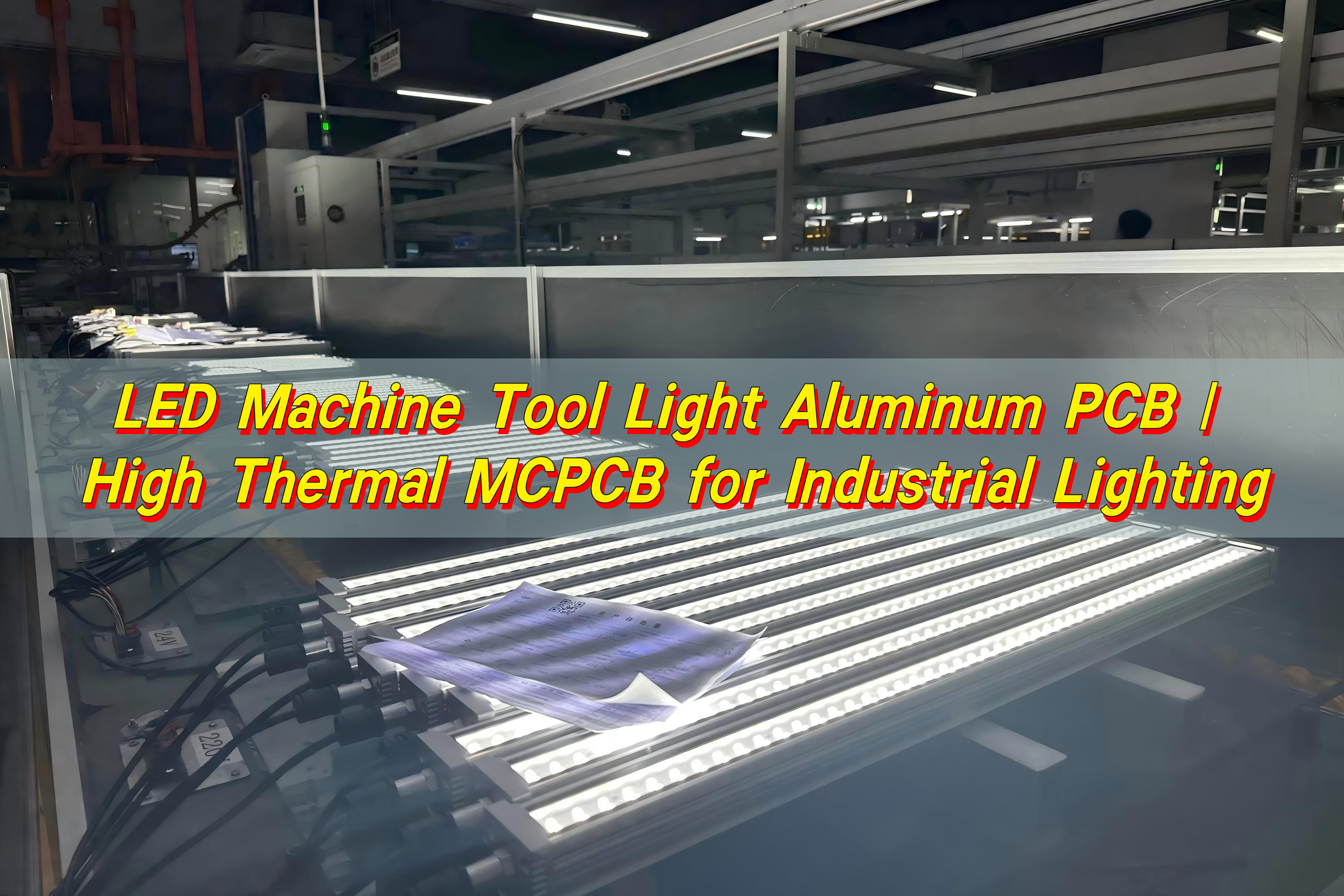
LED Explosion-Proof Light Aluminum PCB is specialized circuit board designed to provide reliable electrical functionality and superior heat dissipation in hazardous environments where flammable gases, vapors, or dust may be present. This article delves into the critical role of these high-thermal-performance Aluminum PCBs, explores common design and manufacturing challenges, and outlines the comprehensive solutions offered by a professional manufacturer.
Are you struggling to balance thermal management, reliability, and performance in hazardous area lighting design?
- Rapid LED Failure: High operating temperatures shorten LED life and accelerate lumen decay.
- Poor Reliability in Harsh Environments: Vibration, thermal cycling, and corrosive conditions can damage solder joints and circuits.
- Signal Integrity Problems: EMI and poor layout can affect driver and control stability.
- High Power Density: Compact fixtures with high-power LEDs create concentrated heat that is difficult to release.
- Complex Supply Chain: Managing PCB fabrication, component sourcing, assembly, and quality across multiple vendors increases risk and delays.
Targeted Solutions
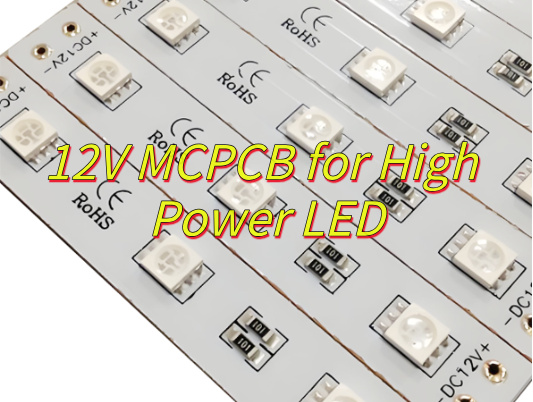
- Better Thermal Management: Aluminum-based MCPCB with high thermal conductivity helps transfer heat away from LEDs quickly.
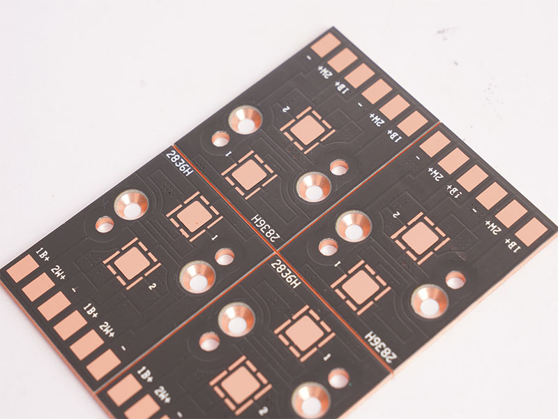
- Stronger Reliability: Heavy copper, precise processing, and durable finishes such as ENIG or ENEPIG improve resistance to heat and corrosion.
- Stable Electrical Performance: Controlled impedance and optimized stack-up reduce noise and support stable circuit operation.
- High-Current Capability: Heavy copper PCBs support power LED current demands without trace overheating.
- One-Stop Manufacturing: Integrated service covering PCB fabrication, parts sourcing, assembly, and testing simplifies the whole project.
At EBest Circuit (Best Technology), we specialize in overcoming these exact challenges. With over 19 years of experience as a full turnkey PCB and PCBA manufacturer, we have the expertise to produce reliable, high-performance Aluminum PCBs for demanding applications like explosion-proof lighting. Our in-house capabilities span design, fabrication of specialized PCBs (including MCPCBs up to 10 layers), precision SMT assembly (handling 01005 components and 0.25mm BGA pitch), and comprehensive testing. We are committed to quality, holding certifications like ISO 9001:2015 and IATF 16949, and guarantee on-time delivery. For your next hazardous area lighting project, pls feel free to contact our experts at sales@bestpcbs.com.
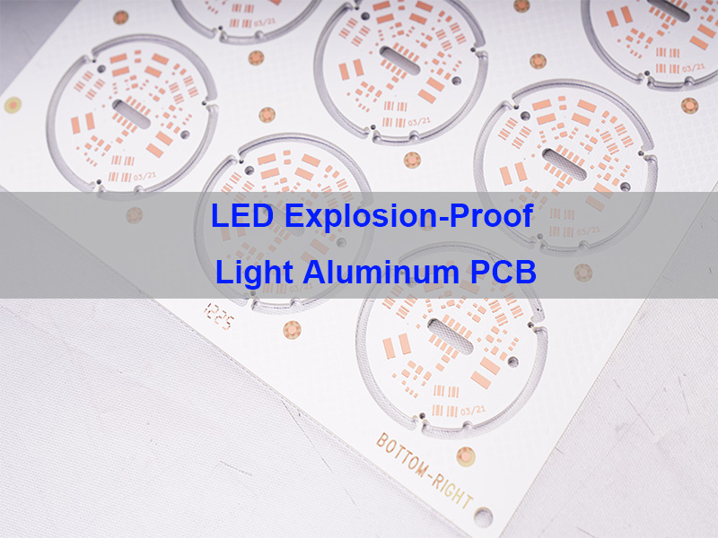
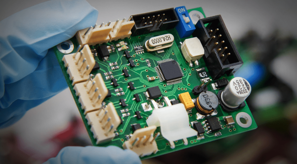
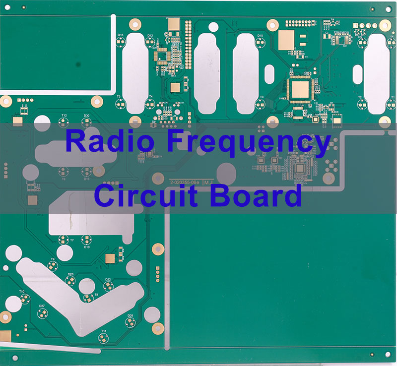
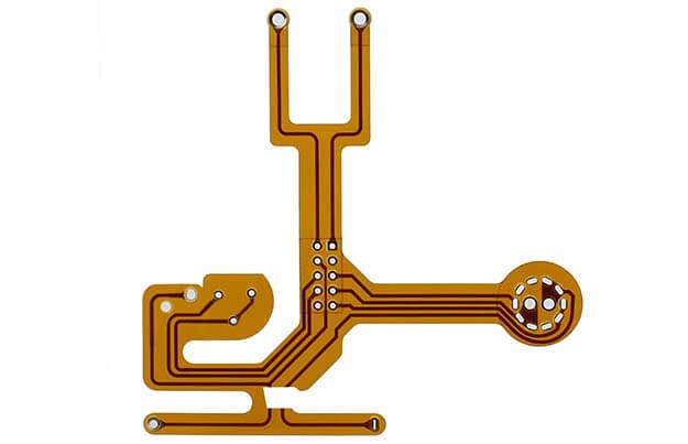
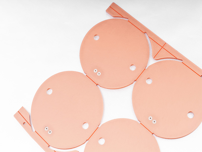
Understanding Aluminum PCB: The Thermal Backbone of LED Explosion-Proof Lights
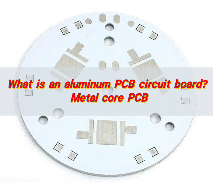
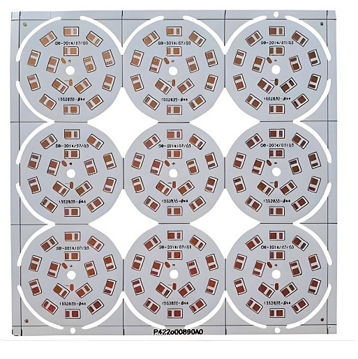
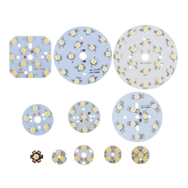
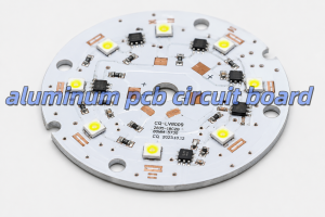
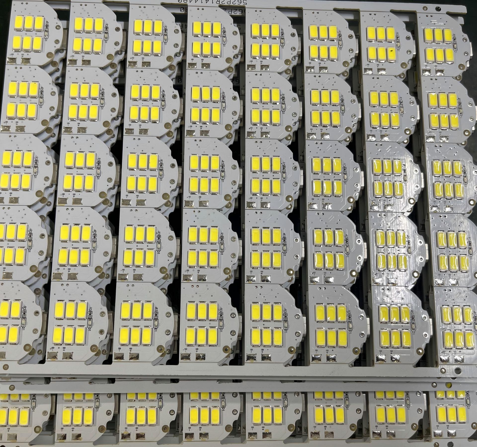
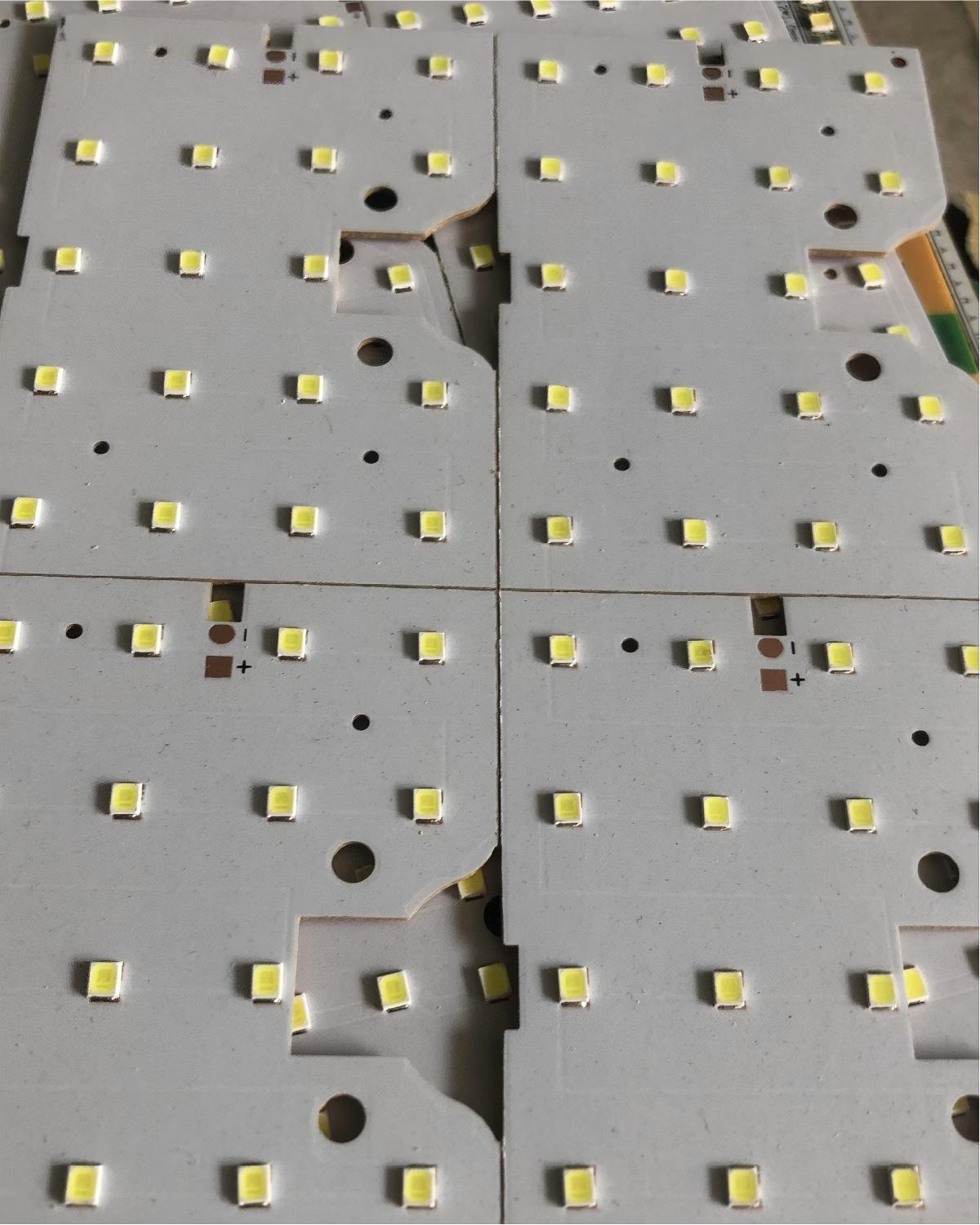
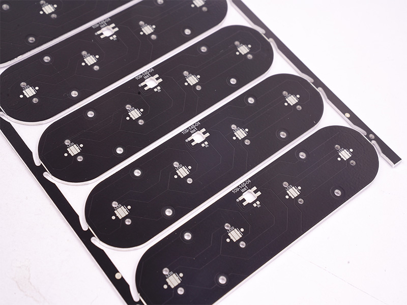
An Aluminum PCB, or Metal Core PCB (MCPCB), is the foundation for managing heat in high-power LED systems. Its unique structure features a dielectric thermally conductive layer bonded to an aluminum substrate, creating an efficient path for heat transfer from the LED chips to the housing and external environment. This is non-negotiable in explosion-proof lights, where maintaining a low junction temperature is critical for LED longevity, color stability, and, most importantly, preventing any surface from exceeding safe temperature limits in a hazardous atmosphere.
Key Advantages of Aluminum PCB for Hazardous Area Lighting:
- Excellent Heat Dissipation: Far superior to standard FR4, it prevents thermal throttling and failure.
- Enhanced Durability: The aluminum base provides mechanical strength and resistance to vibration.
- Space Efficiency: Allows for more compact designs by replacing bulky external heatsinks in some cases.
- Simplified Assembly: Often integrates the mounting surface for LEDs and drivers into a single, robust structure.
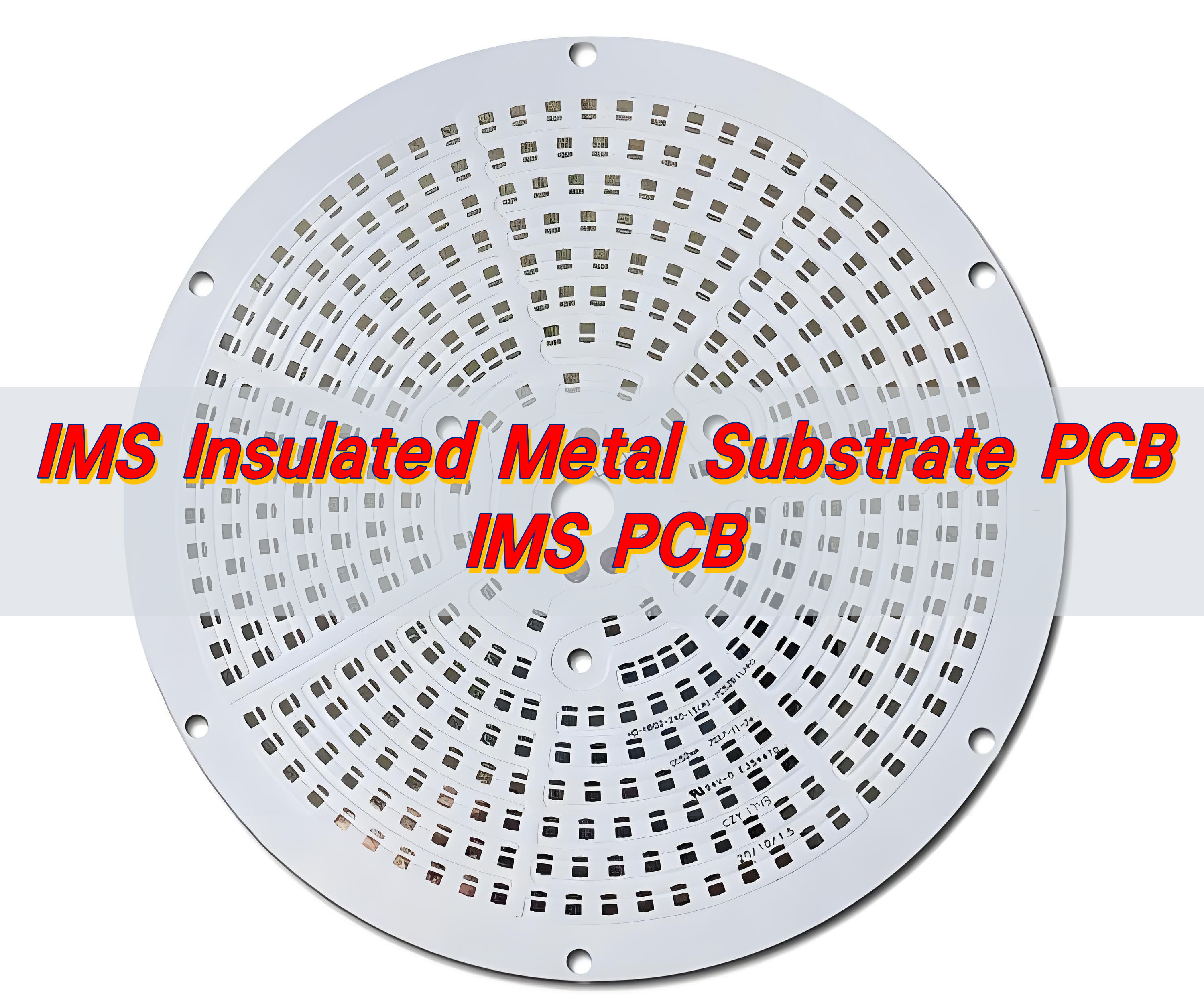
Capability Snapshot for Aluminum PCB (MCPCB):
| Parameter | Capability |
|---|---|
| Max Layers | Up to 10 Layers |
| Base Material | Aluminum, Copper core |
| Max Board Size | 610mm x 1625mm |
| Max Conductor (Copper) Thickness | Up to 10 oz |
| Dielectric Strength | >1.5 KV/mm (L/S>1.5mm) |
| Thermal Conductivity | Standard: 0.8-1.0 W/m·K; High: up to 2.0, 3.0 W/m·K |
In summary, the Aluminum PCB for LED Explosion-Proof Lights is not just a circuit carrier but an active thermal management component. Its ability to efficiently transfer heat is the first line of defense in ensuring the light’s reliability and safety, making the choice of a capable High Thermal Aluminum PCB for Hazardous Areas manufacturer paramount.
Why Aluminum PCBs are Critical for Hazardous Area Compliance?
Explosion-proof certifications (like ATEX, IECEx, UL) mandate strict limits on surface temperatures. The primary role of the Aluminum PCB in Explosion-Proof Lights is to ensure the LED junction temperature, and consequently the exposed surface temperature of the fixture, remains below the auto-ignition point of the specific gas or dust present. Failure to do so can compromise the intrinsic safety of the entire assembly. Therefore, the PCB’s thermal performance is directly tied to certification success and operational safety.
How a High-Performance Aluminum PCB Ensures Compliance:
- Temperature Control: Efficiently moves heat from LEDs to the fixture’s heatsink, maintaining safe surface temps.
- Material Suitability: Uses high-Tg materials and stable dielectrics that can withstand long-term thermal cycling without degradation.
- Reliable Connections: Employs surface finishes like Immersion Gold (ENIG) or ENEPIG, which offer excellent shelf life and solderability for robust, failure-resistant joints.
- Robust Construction: Supports heavy copper designs (e.g., 4-6 oz) for power traces, reducing resistive heating within the board itself.
- Precision Manufacturing: Adheres to tight tolerances (e.g., ±3mil for PTH holes) to ensure consistent electrical and thermal performance across all units.
Ultimately, using a purpose-built Explosion-Proof Light PCB is a critical design decision for compliance. It transforms the design challenge from merely “making it work” to “guaranteeing it works safely under specified conditions,” providing the necessary evidence for certification bodies.
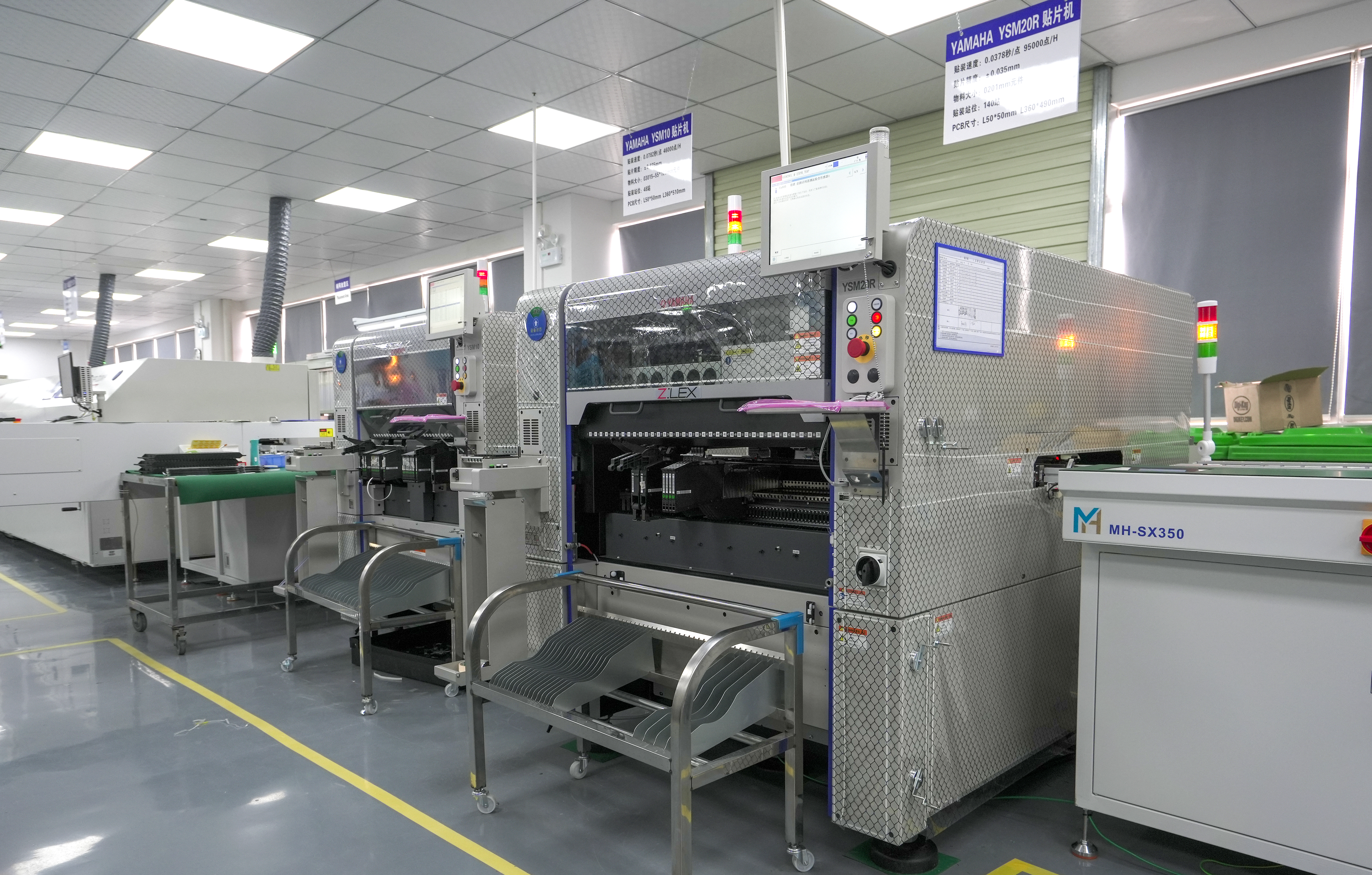
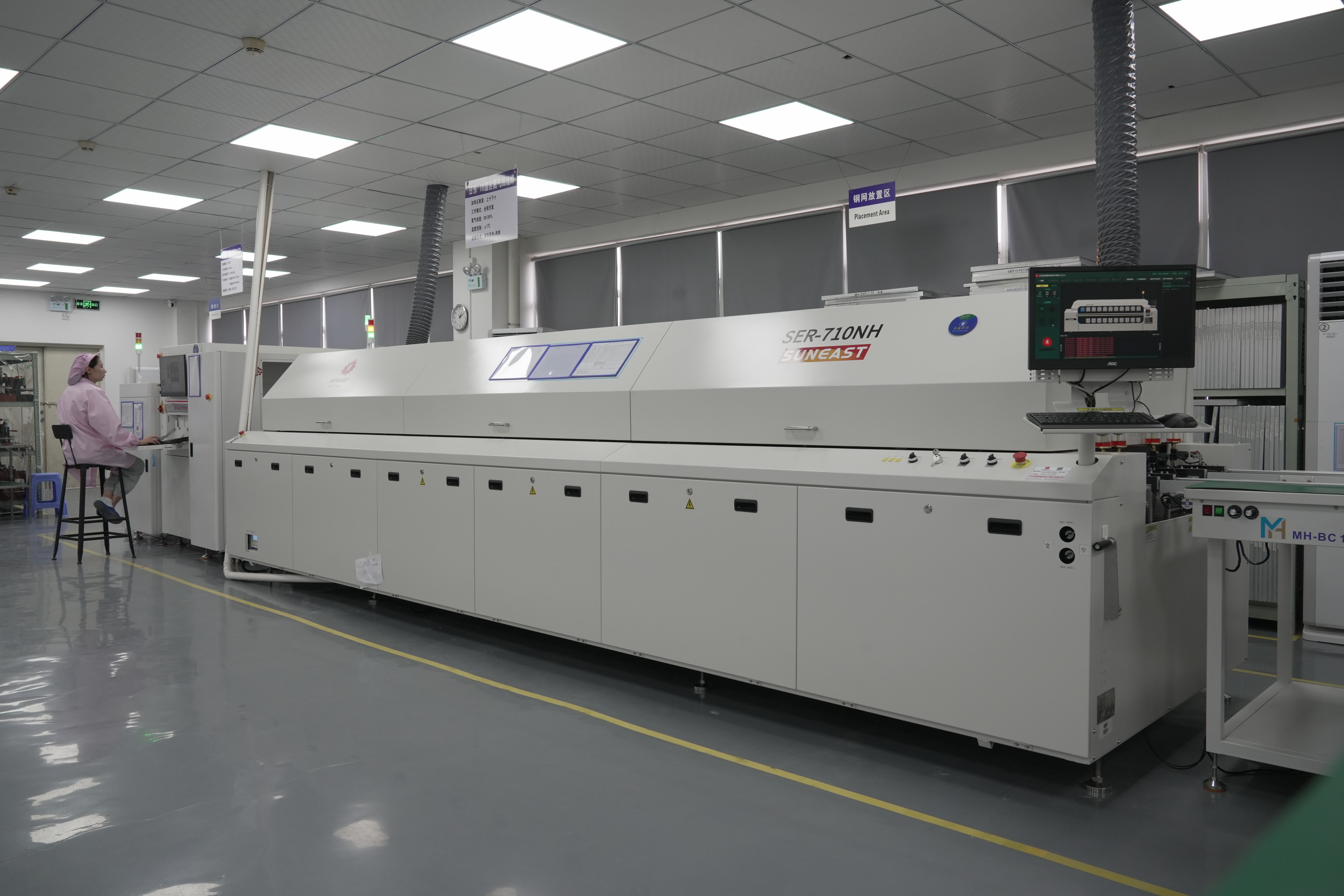
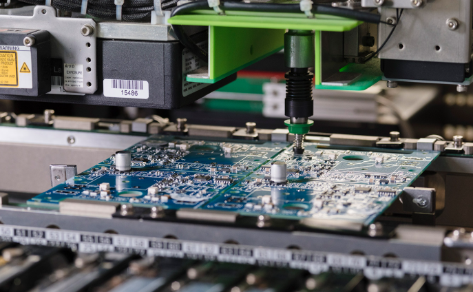
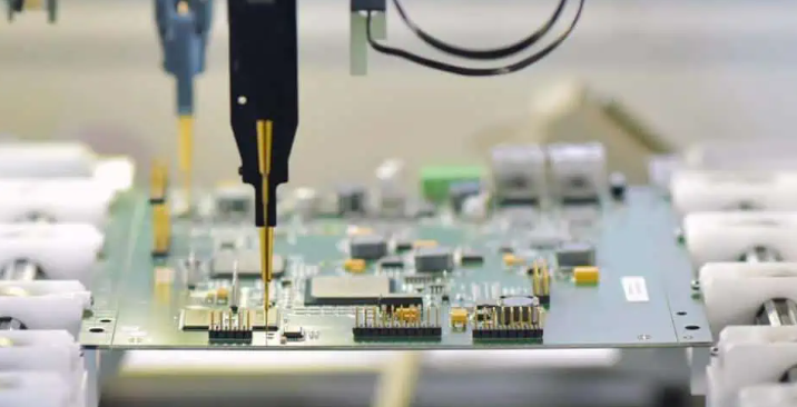
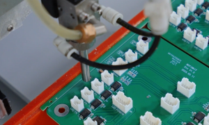
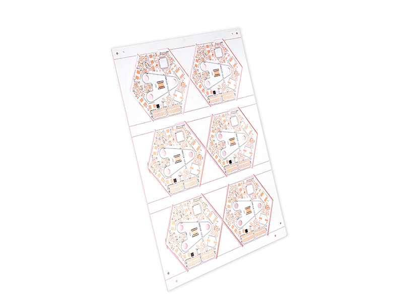
Manufacturing Capabilities for High-Reliability Aluminum PCBs
Producing an Aluminum PCB that meets the stringent demands of hazardous locations requires specialized manufacturing capabilities. It goes beyond standard PCB fabrication to include precise thermal material handling, controlled lamination processes, and rigorous testing. At EBest Circuit, our factory is equipped to handle the entire spectrum, from simple single-layer boards to complex multi-layer Aluminum PCB for High-Power LED designs.
Our Core Manufacturing Capabilities for Your Project:
| Capability Category | Specific Parameters |
|---|---|
| Board Construction | Layers: 1-10L. Types: Standard Aluminum, Copper Core, COB, SinkPAD. |
| Thermal & Electrical | Copper Thickness: 0.5oz – 10oz. Dielectric Strength: >1.5 KV/mm. Min Trace/Space: 6/6 mil. |
| Precision & Reliability | Min Hole Diameter: 12 mil. PTH Wall Thickness: 0.59 mil. Aspect Ratio: Up to 10:1. Surface Finish: HASL, ENIG, OSP, Immersion Silver/Tin. |
| Testing & Inspection | AOI, Flying Probe Test, X-Ray Inspection, Impedance Test, Functional Test. |
We leverage state-of-the-art equipment, such as CNC drill machines, automatic plating lines, and X-Ray copper thickness testers, to ensure every High Thermal Aluminum PCB for Hazardous Areas meets precise specifications. Our expertise in thermal management materials and processes ensures your board will perform reliably, making us a trusted partner for your Explosion-Proof Light Aluminum PCB needs.
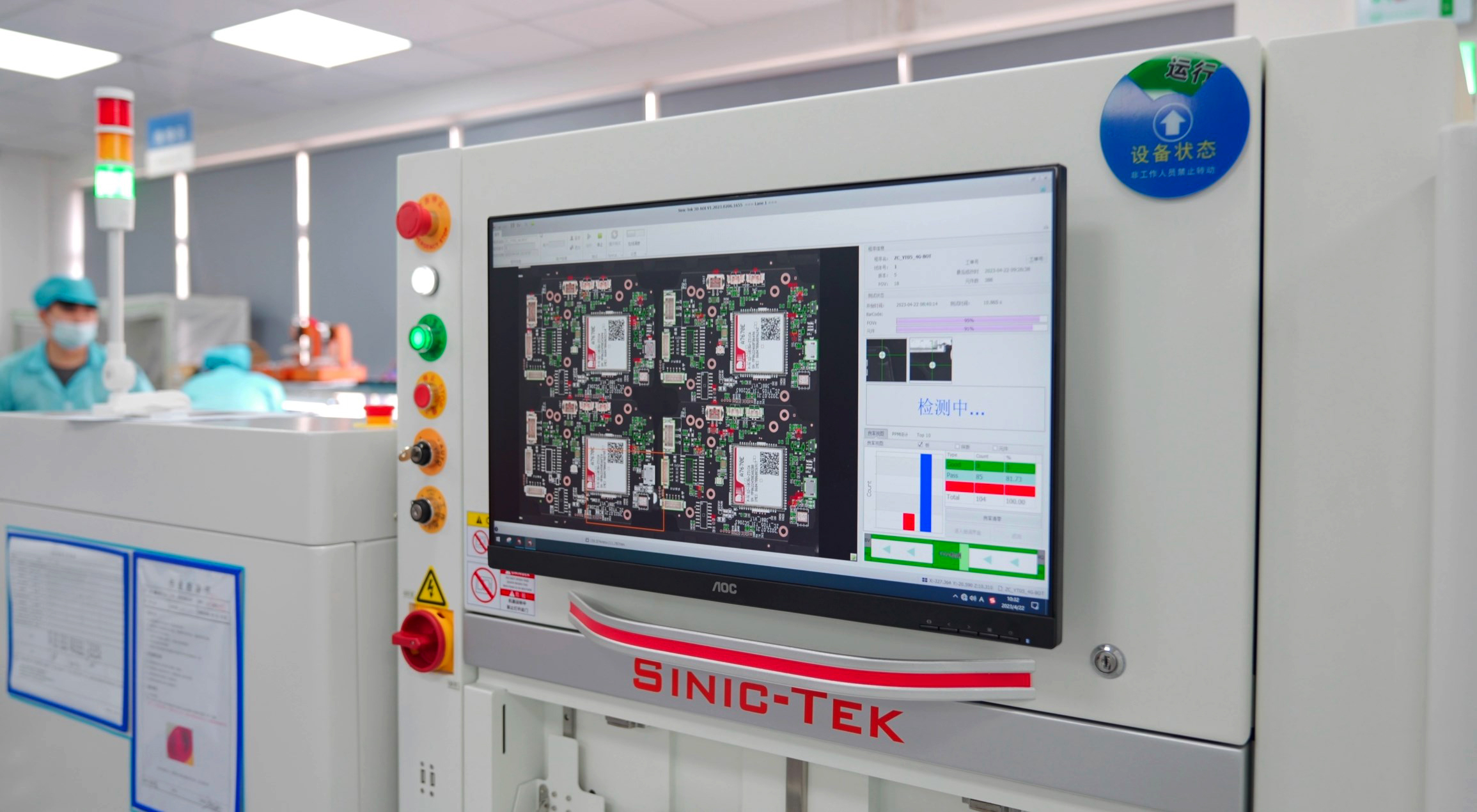
Quality Control and Testing: Ensuring Reliability in Every Board
For explosion-proof applications, quality cannot be an afterthought; it must be built into every stage. Our quality control protocol is designed to catch potential failures before they happen, ensuring that every High Thermal Aluminum PCB shipped is capable of performing in the field. We adhere to IPC standards and employ a multi-step inspection regimen.
Our Multi-Stage Quality Assurance Process:
- Incoming Material Inspection: Verification of aluminum substrate, dielectric layer, and copper foil quality.
- In-Process Control (IPC): Real-time monitoring during drilling, etching, and lamination.
- Electrical Testing: 100% electrical test for opens and shorts using Flying Probe or Universal E-Testers.
- Thermal Reliability Testing: Thermal stress tests (e.g., 3x 10 sec @ 280°C) to simulate soldering and operational cycling.
- Final Audit: Dimensional check, visual inspection under AOI, and verification of surface finish.
This rigorous approach, backed by certifications like ISO 9001:2015 and IATF 16949, guarantees that the Aluminum PCB for LED Explosion-Proof Lights you receive is not just functional, but exceptionally reliable and built to last in demanding environments.
Design Guidelines and Best Practices
A successful Explosion-Proof Light PCB design harmonizes electrical, thermal, and mechanical requirements. Following best practices from the outset can prevent costly redesigns and ensure manufacturability. Collaboration with your PCB manufacturer early in the design phase is highly recommended.
Key Design Considerations for Optimized Aluminum PCBs:
- Thermal Via Arrays: Place a grid of vias under high-power LED pads to enhance heat transfer to the aluminum base. For MCPCBs, this often involves non-plated holes filled with thermal paste.
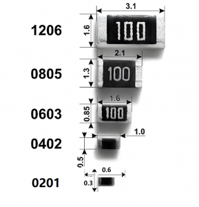
- Copper Weight: Use heavier copper (2oz or more) for high-current traces to reduce resistance and self-heating. We can support up to 10oz copper on Aluminum PCBs.
- Component Placement: Keep thermally sensitive components, like drivers, away from the hottest areas of the board. Consider using the aluminum base as a physical heatsink.
- Solder Mask & Finishes: Specify a thermally stable solder mask. For the best solderability and shelf life in critical applications, choose ENIG or ENEPIG.
- DFM (Design for Manufacturability) Check: Submit your design for a DFM analysis. We can review specifics like trace/space (min 6/6 mil for MCPCB), annular rings, and pad sizes to ensure a smooth production process.
By integrating these guidelines, you create a design that is not only electrically sound but also optimized for thermal performance and reliable manufacturing, resulting in a robust Aluminum PCB for High-Power LED systems.
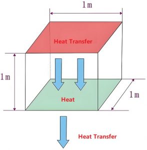
Where Does the Heat Really Go in an Aluminum PCB Structure?
In an explosion-proof LED fixture, heat does not simply “dissipate”—it follows a defined thermal path. Understanding this path is critical to controlling junction temperature and ensuring long-term stability.
The heat generated at the LED junction first transfers into the copper pad, then passes through the dielectric layer, and finally spreads across the aluminum base before being released into the housing and ambient environment.
However, not all layers contribute equally:
- Copper Layer:
Acts as the initial heat spreader. Thicker copper (2oz–4oz) helps distribute localized heat more evenly, reducing hotspots. - Dielectric Layer (Critical Bottleneck):
This is often the weakest link in the thermal chain. Even with aluminum underneath, poor dielectric conductivity can trap heat.
For hazardous lighting, materials with ≥2.0 W/m·K are commonly preferred. - Aluminum Base:
Serves as the main heat sink, rapidly spreading heat laterally. Thickness (typically 1.0–2.0mm) directly affects thermal capacity.
In high-power designs, standard MCPCB may not be sufficient. Direct Thermal Path (DTP / SinkPAD) structures are often introduced to eliminate dielectric resistance under the LED, creating a near-direct heat channel to the aluminum core.
The key takeaway:
Thermal performance is not defined by aluminum alone, but by how efficiently each layer transfers heat in sequence.
What Makes a PCB Truly Reliable in Sealed, Hazardous Enclosures?
Reliability in hazardous environments is not just about material strength—it is about how the PCB behaves under continuous stress inside a sealed system.
Unlike open-air designs, explosion-proof fixtures trap heat, moisture, and pressure variations. This creates compounded stress on both materials and interconnections.
Several factors define true reliability:
- Thermal Cycling Resistance:
Repeated heating and cooling cause expansion mismatch between copper, dielectric, and aluminum.
A well-matched CTE structure reduces solder joint fatigue and layer separation. - Dielectric Stability Over Time:
Low-quality dielectric materials degrade under high temperature, leading to insulation failure.
High Tg and stable thermal conductivity are essential for long service life. - Surface Finish Durability:
Finishes like ENIG or ENEPIG provide better resistance against oxidation and corrosion, especially in humid or chemically aggressive environments. - Mechanical Integrity:
Vibration and installation stress require strong adhesion between layers and robust pad design to prevent cracking or delamination. - Electrical Stability:
Controlled impedance and proper grounding help avoid EMI-related instability, especially in driver circuits within compact enclosures.
In practice, reliability is achieved when thermal, mechanical, and electrical designs are aligned—not treated separately.
To wrap up, LED Explosion-Proof Light Aluminum PCBs are indispensable components that ensure safety, longevity, and performance in volatile environments by mastering the critical challenge of heat dissipation. This article has explored their vital role, addressed key design and manufacturing pain points, and presented targeted solutions.
When your project demands uncompromising quality and reliability, partnering with an experienced manufacturer is essential. EBest Circuit (Best Technology) offers a full turnkey solution—from design support and advanced Aluminum PCB in Explosion-Proof Lights fabrication to component sourcing, precise assembly, and rigorous testing. We combine two decades of expertise with a commitment to competitive pricing and on-time delivery. Pls feel free to contact us anytime at sales@bestpcbs.com for a quote or consultation.
FAQs About LED Explosion-Proof Light Aluminum PCB
1. Why are aluminum PCBs preferred in explosion-proof LED lighting?
They provide efficient heat dissipation, which is essential in sealed enclosures where heat cannot escape easily. This helps maintain LED performance and prevents thermal-related failures.
2. What thermal conductivity should the dielectric layer have?
For most hazardous lighting applications, 1.5–3.0 W/m·K is typical, with higher values recommended for high-power or dense LED layouts.
3. Is standard MCPCB enough for high-power explosion-proof lights?
Not always. For higher power densities, DTP (Direct Thermal Path) designs are often required to reduce thermal resistance and improve heat transfer efficiency.
4. How thick should the aluminum base be?
Common thickness ranges from 1.0mm to 2.0mm, depending on mechanical strength and thermal requirements. Thicker bases improve heat spreading but increase weight.
5. What surface finish is best for harsh environments?
ENIG and ENEPIG are widely used due to their corrosion resistance and stable solderability over time.
6. Can aluminum PCBs handle high current?
Yes, especially when combined with heavy copper (2oz–4oz or more). Proper trace design is still required to avoid overheating.