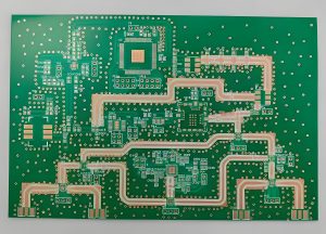
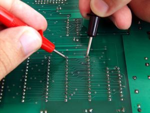
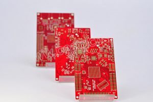
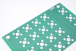
AOI, or Automated Optical Inspection, is a process in PCB manufacturing that utilizes advanced imaging technology to inspect PCBs for potential defects. During the inspection, cameras capture detailed images of the PCB at different stages, comparing them against predefined standards to ensure every component is correctly placed and connected. AOI serves as a crucial step, helping detect manufacturing flaws that could lead to functional issues.
What is an AOI Machine in PCB?
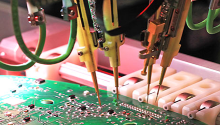
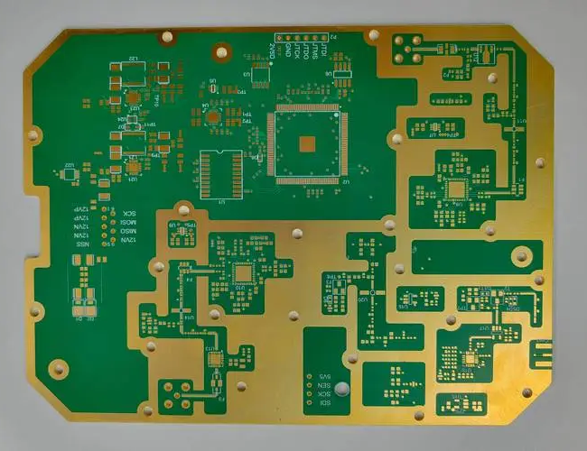
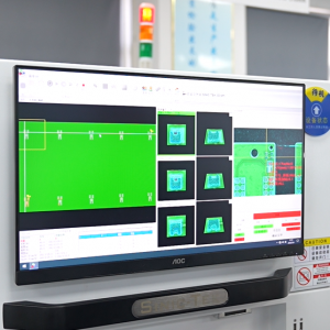
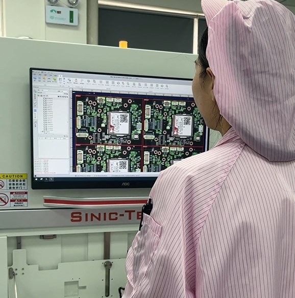
AOI machine is a kind of inspection equipment based on optical principle, mainly used to detect various defects on a PCB board. The AOI device automatically scans the PCB through a high-definition CCD camera, acquires images, and compares the tested solder joints with qualified parameters in the database. After image processing, the defects on the PCB are checked, and the defects are displayed through the display or automatic signs for repair personnel to correct.
AOI detection is mainly composed of light source and its control subsystem, digital imaging and its control subsystem (including CCD/CMOS camera, image acquisition), image scanning motion mechanism and its control subsystem, image processing and optimization subsystem, image feature recognition and defect recognition subsystem, HMI and main control subsystem. These subsystems work together to scan the PCB and obtain the PCB image by controlling the light source, digital imaging, scanning and other subsystems, and then register the processed PCB image with the PCB standard image, extract features and compare and analyze the processed PCB image to determine whether the PCB has defects and the type of defects, and identify the location of defects.
What is the Basic Principle of AOI?
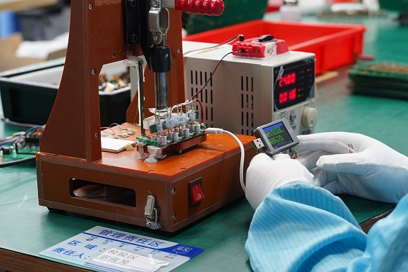
The principle behind AOI is quite straightforward: it illuminates the PCB through the light source, uses the optical lens to collect the reflected light of the PCB into the computer, and analyzes the color difference or gray ratio of the PCB information through the computer software, so as to judge the solder paste printing on the PCB, component placement, solder joint welding quality and so on. The AOI system can also analyze and count the defects to provide a basis for adjusting the process parameters of the manufacturing process.
In another word, it relies on optical imaging and pattern recognition to detect defects. AOI machines are programmed with reference images of a perfect PCB layout. They then scan each PCB, capturing images and comparing them pixel-by-pixel to the reference model. Variations between the scanned image and the reference indicate potential defects, prompting the machine to flag these areas for further review.
What are the Benefits of an AOI Machine?
1. Accuracy in Detection
AOI machines can identify defects that might be overlooked by manual inspection. The precision with which they analyze each PCB ensures high-quality output, reducing errors in the final product.
2. Speed and Efficiency
Automated inspection greatly speeds up the inspection process, especially valuable in large-scale manufacturing. With AOI, hundreds of PCBs can be checked in a fraction of the time required for manual inspection.
3. Cost Reduction
Early detection of defects prevents costly rework or scrap, saving both time and resources. By addressing issues during the early stages, AOI contributes to a smoother production process.
4. Consistency and Reliability
Unlike human inspection, which can vary, AOI provides consistent results every time. It applies the same criteria to every PCB, ensuring uniformity and quality across all batches.
5. Enhanced Quality Control
In a competitive market, high-quality products build trust with clients. AOI enables manufacturers to deliver high-standard PCBs, maintaining quality and reducing potential returns.
What Kinds of Defects Can Be Checked During AOI?
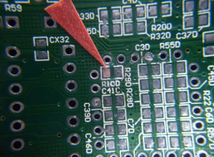
1. Soldering Issues
AOI machines are highly effective in identifying soldering defects, such as insufficient solder, excess solder, or bridging, which can interfere with connectivity.
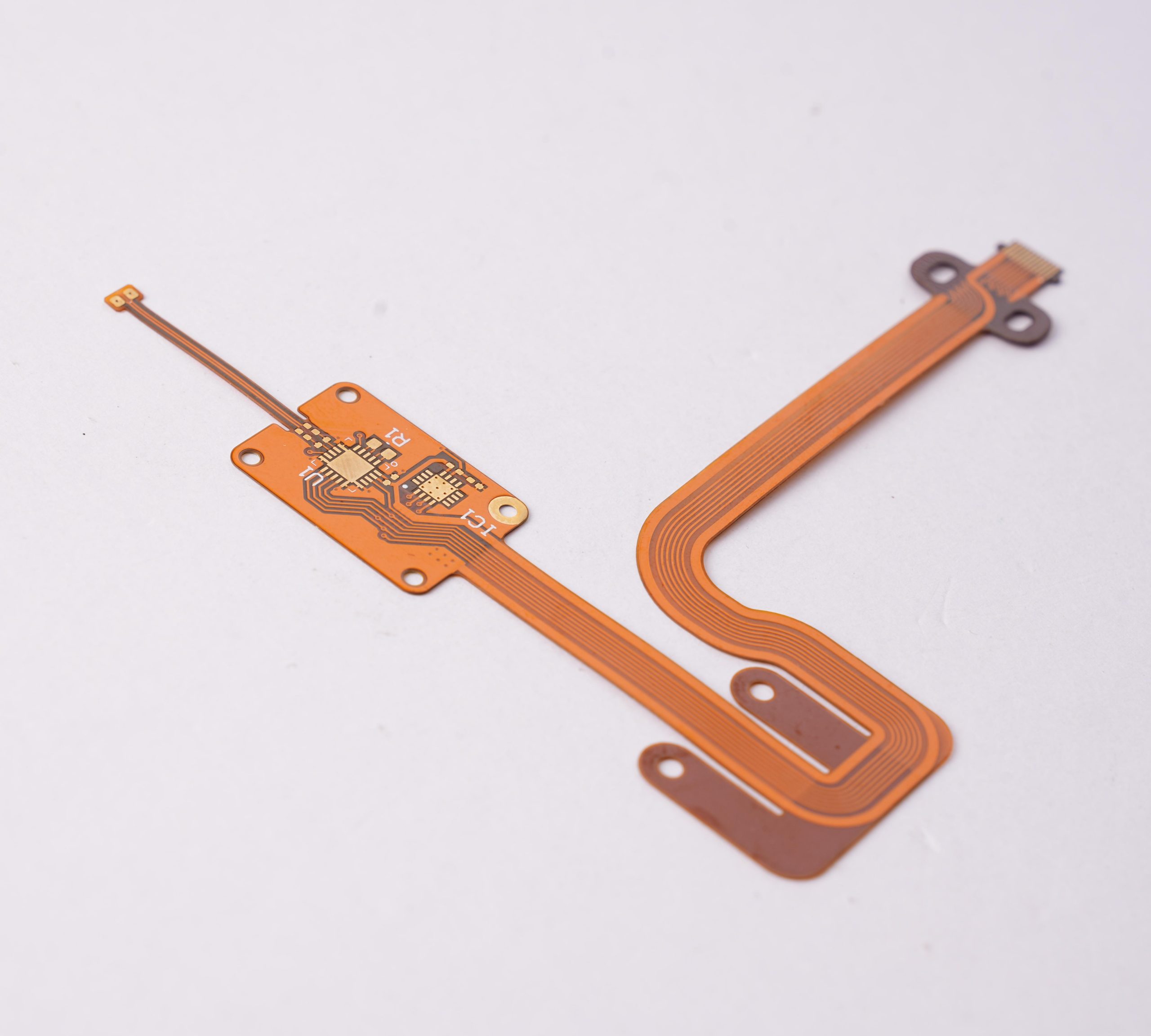
2. Misalignment of Components
AOI can detect misaligned components or misplaced parts, which might cause issues in functionality or even physical interference on the PCB.
3. Component Presence and Orientation
The machine checks if all components are present and correctly oriented. Missing or rotated parts can lead to non-functioning circuits.
4. Short Circuits and Opens
AOI identifies unwanted connections (shorts) and incomplete circuits (opens), ensuring each connection is accurate and functional.
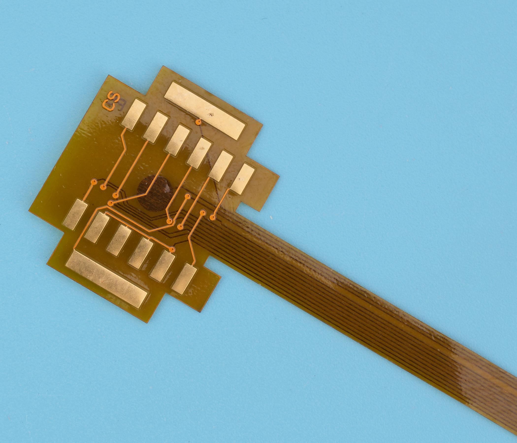
5. Surface Defects
Surface issues, including scratches, contamination, or other irregularities, are also detectable through AOI, contributing to the visual quality of the board.
6. Polarity and Value Verification
Some AOI systems can check component polarity and values, confirming that each component matches the required specifications for the PCB design.
AOI Applications
1. Consumer Electronics Manufacturing
Given the high volume of consumer electronics, AOI’s speed and accuracy are essential for maintaining efficiency without sacrificing quality. It is used for inspecting products like smartphones, laptops, and household appliances.
2. Automotive Industry
In automotive electronics, reliability is critical. AOI helps ensure that safety and performance-related components are defect-free, such as sensors, control units, and in-car entertainment systems.
3. Medical Devices
Medical equipment relies on precision and reliability. AOI in PCB inspection for medical devices ensures that these life-saving tools meet strict standards, minimizing risks in critical applications.
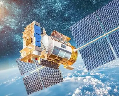
4. Aerospace and Defense
For aerospace and defense, where reliability and durability are paramount, AOI supports quality assurance in sensitive equipment, such as navigation systems and communication devices.
5. Telecommunications
In telecommunications, AOI assists in inspecting high-frequency PCBs, ensuring that communication devices remain operational and effective over long periods.
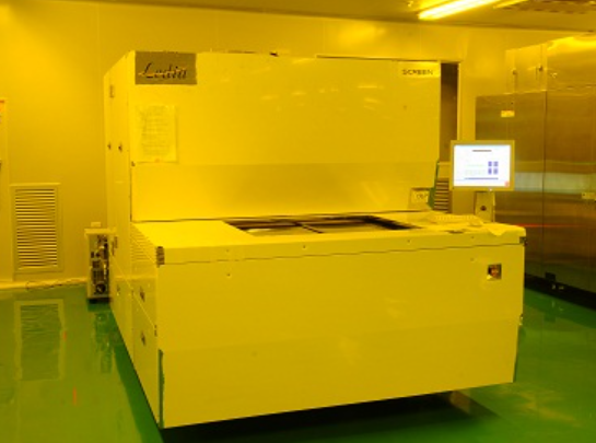
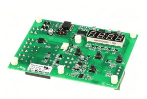
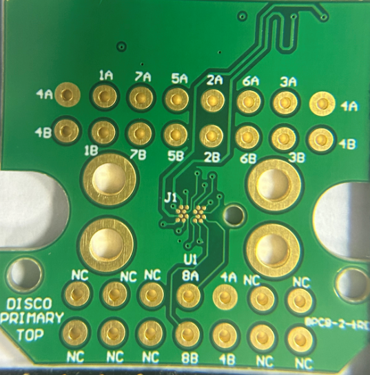
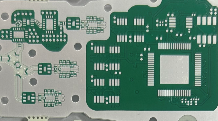
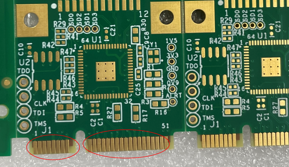
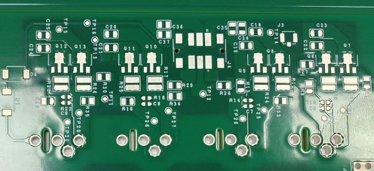
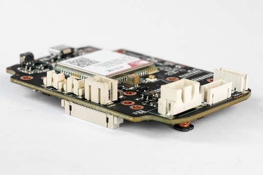
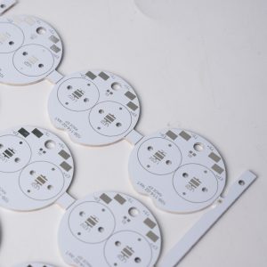
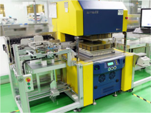
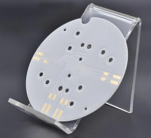
To ensure high quality of PCBA, EBest Circuit (Best Technology) equipped with 3D online AOI to detect PCB defectives from all aspects. Contact us if you have any questions.