PCB manufacturing PCB manufacturing
Home > Blog

IMS PCB Material Selection & Design Guideline

July 22nd, 2025

Are you worried about how to choose IMS PCB material for your project? Let’s explore its definition, properties, datasheet, types, IMS PCB material selection and design guidelines through this blog.

  • Wrong choice of substrate material leads to too high thermal resistance?
  • Is the dielectric layer easy to delaminate during multi-layer IMS design?
  • Is the dielectric loss too large under high-frequency application?

EBest Circuit (Best Technology) Can Provide:

  • Provide 5 standardized thermal conductivity levels (1.5~8W/mK); Free sample matching tool, generate selection report in 30 minutes.
  • Patented resin system, peel strength>1.8N/mm; Support 3-layer lamination process, provide design specification manual.
  • Df value as low as 0.002 (@10GHz); Equipped with HFSS simulation model library, plug-and-play.

Welcome to contact us if you have any request for IMS PCB or MCPCB: sales@bestpcbs.com.

What Is IMS Material?

IMS material, known as insulated metal substrate, consists of a metal core, typically aluminum or copper, coated with a dielectric insulation layer and a conductive copper layer for circuit traces. This structure delivers outstanding thermal management, with aluminum-based versions achieving thermal conductivity of 1-3 W/(mĀ·K), while copper-based variants exceed 400 W/(mĀ·K) for accelerated heat dissipation.

It serves effectively in high-power applications like LED lighting systems and automotive electronics, where efficient cooling maintains device stability and extends operational lifespan under thermal stress.

What Is IMS Material?

IMS PCB Material Properties

  • Thermal Conductivity – Metal base (aluminum/copper) transfers heat 5-10x faster than FR4, keeping components cooler.
  • Electrical Insulation– Dielectric layer provides high voltage isolation (1-10kV) while allowing heat flow.
  • Mechanical Strength – Metal core resists bending/warping, ideal for heavy components or high-vibration environments.
  • Thermal Expansion – Low CTE (Coefficient of Thermal Expansion) matches components, reducing solder joint stress.
  • Temperature Resistance – Withstands 150-250ā„ƒ operating temperatures without degradation.
  • Weight Efficiency – Aluminum bases offer lightweight heat dissipation, crucial for automotive/aerospace.
  • Surface Flatness – Metal substrates ensure precise component mounting, critical for fine-pitch devices.

IMS PCB Board Material Datasheet

PropertyAluminum-Based IMSCopper-Based IMSMeasurement Standard
Thermal Conductivity1-3 W/(mĀ·K)>400 W/(mĀ·K)ASTM E1461
Dielectric Strength≄4 kV/mm≄4 kV/mmIPC-TM-650 2.5.6
CTE (Z-axis)12-15 ppm/°C16-18 ppm/°CIPC-TM-650 2.4.24
Tg (Glass Transition)130-150°C150-170°CIPC-TM-650 2.4.25
Td (Decomposition)300-320°C350-380°CIPC-TM-650 2.3.40
Volume Resistivity≄10¹² Ω·cm≄10¹² Ω·cmIPC-TM-650 2.5.17
Flexural Strength100-150 MPa200-250 MPaIPC-TM-650 2.4.4

What Are Types of IMS PCB Material?

Aluminum-Based IMS

  • Thermal Conductivity: 1-2.5W/mĀ·K.
  • Application: LED lighting, consumer power supplies, and automotive controls where cost efficiency and moderate heat dissipation are prioritized.

Copper-Based IMS

  • Thermal Conductivity: 3-4W/mĀ·K.
  • Application: High-power industrial drives, automotive powertrains, and aerospace components requiring extreme thermal performance.

Stainless Steel-Based IMS

  • Thermal Conductivity: 0.2-0.5W/mĀ·K.
  • Application: Corrosive environments (e.g., marine, chemical processing) where mechanical durability outweighs thermal needs.
Composite Metal Core IMS

  • Structure: Aluminum/copper layer bonded to a thin copper circuit layer.
  • Application: Compact devices like mobile chargers and RF amplifiers needing both heat spreading and fine-pitch circuitry.
What Are Types of IMS PCB Material?

How to Choose IMS PCB Material?

IMC PCB Material Selection Guideline:

1. Assess Power Density Requirements

  • High-Power Applications (e.g., industrial drives, automotive power modules):
  • Choose copper-based IMS (thermal conductivity 3-4W/mĀ·K) for power densities exceeding 5W/cm².
  • Standard Applications (e.g., LED lighting, consumer electronics):
  • Prioritize aluminum-based IMS (1-2.5W/mĀ·K) for power densities below 5W/cm².

2. Align with Budget Constraints

  • Aluminum-based IMS costs 20-30% less than copper, making it suitable for cost-driven projects like household appliances.
  • Reserve copper-based IMS for premium sectors (aerospace, medical devices) where long-term reliability outweighs upfront costs.

3. Match Environmental Conditions

  • Corrosive Environments (marine, chemical processing): Select stainless steel-based IMS for corrosion resistance, despite lower thermal efficiency.
  • High-Temperature Zones (engine compartments, RF amplifiers): Use copper-based IMS with polyimide insulation (withstanding temperatures >200°C).

4. Account for Spatial Limitations

  • Compact Devices (mobile chargers, wearables): Choose aluminum composite IMS (0.8mm thickness) to balance heat dissipation and space efficiency.
  • Multi-Layer Designs: Prioritize copper-based IMS for structural rigidity, preventing warping in complex PCB stacks.

5. Validate Compliance with Standards

  • Critical Systems (automotive ECU, aerospace): Demand IPC-6013-certified copper-based IMS with documented thermal cycling test results.
  • Consumer Products (TVs, monitors): Aluminum-based IMS meets 85°C operational requirements for typical use cases.

6. Decision-Making Framework

  • Start with power density thresholds to narrow material options.
  • Cross-reference with budget allocation and environmental exposure.
  • Finalize with space constraints and certification needs.
7. Application Examples

  • Industrial Motor Control: Copper-based IMS for sustained 100A+ current handling.
  • Outdoor LED Displays: Aluminum-based IMS with conformal coating for humidity resistance.
  • Automotive Powertrain: Copper-based IMS + high-temperature dielectric for under-hood reliability.

8. Critical Precautions

  • Request third-party thermal resistance reports to verify supplier claims.
  • Avoid materials with unspecified dielectric breakdown voltage in high-voltage applications.
  • Test prototypes under real-world thermal stress before mass production.

How to Design IMS PCB Board?

IMS PCB Design Guideline:

1. Define Design Objectives

  • Clarify power density (W/cm²), operating environment (temperature/humidity), space limits, and budget. Example: Automotive ECU board needing 50A current handling in 100°C engine bay.

2. Material Selection Recap

  • High-Power (>5W/cm²): Copper-based IMS (3-4W/mĀ·K).
  • Cost-Sensitive: Aluminum-based IMS (1-2.5W/mĀ·K).
  • Corrosive Environments: Stainless steel-based IMS.

3. Layer Stackup Design

  • Place metal base directly below high-power components.
  • Keep dielectric layer thickness ≤100µm for optimal thermal performance.
  • Example: 2-layer IMS (copper base + 35µm circuit layer).

4. Thermal Management Strategies

  • Thermal Vias: Use 0.5mm diameter filled vias under hot components, spaced 1mm apart.
  • Reserved Cooling Zones: Allocate 30-50% of board area as unpopulated metal regions.
  • Component Placement: Center power devices (MOSFETs/IGBTs) over the metal core; keep ≄2mm spacing between high-power parts.

5. Electrical Layout Optimization

  • Trace Width: Use 3oz (105µm) copper for traces carrying >50A. Widen traces by 2x near heat sources.
  • Avoid Sharp Bends: Maintain ≄3x trace width for bend radii to reduce resistance.
  • Impedance Control: For RF/high-speed signals, keep dielectric thickness consistent (±10µm tolerance).

6. Manufacturing Compatibility

  • Design Rules: Minimum trace width/spacing ≄0.2mm for aluminum IMS; ≄0.15mm for copper IMS.
  • Solder Mask: Remove mask in thermal zones to maximize metal exposure.
  • Panelization: Add 2mm border around boards for handling during assembly.

7. Validation & Testing

  • Thermal Imaging: Test under max load to identify hotspots. Junction temp should stay ≤85°C.
  • Electrical Testing: Verify current capacity and signal integrity (e.g., <5% voltage drop).
  • Reliability Testing: Conduct thermal cycling (-40°C to +125°C, 100 cycles) and vibration tests (2G RMS).
How to Design IMS PCB Board?

IMS PCB Board Design Considerations

Thermal Managementā€Œ

  • Base Material Selectionā€Œ: Aluminum (1-3 W/mK) suits cost-sensitive, moderate-heat applications like LED lighting. Copper (>400 W/mK) is ideal for high-power modules requiring rapid heat dissipation.
  • Dielectric Thicknessā€Œ: Thinner layers (50-100μm) improve heat transfer but reduce voltage isolation. Match thickness to operational voltage (e.g., 100μm for <1kV).
  • Component Placementā€Œ: Position high-heat components (e.g., power ICs, LEDs) directly over the metal core to maximize thermal path efficiency.

Electrical Performanceā€Œ

  • Trace Width/Spacingā€Œ: Wider traces reduce resistance for high-current paths. Maintain ≄0.3mm spacing for 1kV isolation in standard designs.
  • Via Usageā€Œ: Avoid thermal vias in the dielectric layer, they disrupt heat flow. Route signals through peripheral non-metal zones.
  • High-Frequency Limitsā€Œ: IMS materials exhibit higher dielectric loss than FR-4. Limit use in RF circuits (>500MHz).

Mechanical Designā€Œ

  • Board Thicknessā€Œ: Standard metal cores (1.0-3.0mm) prevent flexing but increase weight. For lightweight needs, consider 1.0mm aluminum.
  • Mounting Hardwareā€Œ: Use insulated standoffs to prevent short circuits with the metal base. Account for CTE mismatch, aluminum expands 23ppm/°C versus 17ppm/°C for copper.
  • Cutouts & Edgesā€Œ: Smooth, rounded edges minimize stress concentrations. Internal cutouts require laser processing to avoid burrs.

Manufacturing & Costā€Œ

  • Fabrication Toleranceā€Œ: IMS requires specialized drilling (carbide bits) due to metal hardness. Allow ±0.1mm for hole positioning.
  • Panel Utilizationā€Œ: Standard panel sizes (18″Ɨ24″) optimize cost. Odd shapes increase waste.
  • Finish Optionsā€Œ: HASL is cost-effective but limits thermal performance. ENIG (Ni/Au) enhances solderability for fine-pitch components.

Application-Specific Tipsā€Œ

  • LED Arraysā€Œ: Use 1.5mm aluminum cores with 80μm dielectric to balance cost and heat dissipation (Ī”T<15°C at 5W/cm²).
  • Automotive Invertersā€Œ: Copper cores with 150μm dielectric handle 10-15A/mm² current density and 125°C ambient temperatures.
  • Aerospaceā€Œ: Stainless steel bases provide vibration resistance but require thermal interface materials (TIMs) to offset lower conductivity.
IMS PCB Board Design Considerations

How to Select A Reliable IMS PCB Manufacturer?

Tips for selecting a reliable IMS PCB manufacturer:

  • Confirm Thermal Management Expertiseā€Œ: Verify experience with aluminum/copper cores and UL-certified dielectric materials for effective heat dissipation in high-power applicationsā€Œ.
  • Demand Precision Manufacturing Capabilitiesā€Œ: Ensure ≤50μm laser drilling accuracy for microvias and tight tolerances (±25μm) critical for thermal performanceā€Œ.
  • Require Relevant Quality Certificationsā€Œ: Prioritize IATF 16949 (automotive) or ISO 13485 (medical) certified suppliers with documented thermal cycling tests (-40°C to +150°C)ā€Œ.
  • Evaluate True Production Speedā€Œ: Compare realistic lead times. Proven manufacturers deliver prototypes in 7 days, 30% faster than industry norms without compromising qualityā€Œ.
  • Insist on Transparent Costingā€Œ: Avoid hidden fees. Competitive suppliers offer fixed pricing with 5-15% savings through efficient material utilizationā€Œ.
  • Check Scalability from Prototype to Volumeā€Œ: Choose partners handling orders from 5 panels to mass production seamlessly within their facilitiesā€Œ.
  • Prioritize Technical Partnershipā€Œ: Select manufacturers providing free 24-hour DFM feedback and thermal simulation support to optimize your designā€Œ.
  • Experience the EBest Circuit (Best Technology) Advantageā€Œ: Get a rapid quote for your IMS PCB project today. We combine certified quality, 7-day prototype turnaround, and cost-competitive pricing—ensuring your thermal management solution excels. Request your quote now.

Ready to start your project?ā€Œ Contact ā€ŒEBest Circuit (Best Technology)ā€Œ today for competitive pricing, guaranteed fast delivery, and certified quality. Let’s optimize your thermal management solution together: sales@bestpcbs.com.

You may also like

IMS PCB Definition: 3 Key Focus & 80% Better Thermal

July 22nd, 2025

IMS PCB definitionĀ refers to a printed circuit board built on an Insulated Metal Substrate, primarily designed for excellent heat dissipation. This structure supports high-power components and keeps temperatures under control. While many boards rely on FR4, IMS stands out where thermal stress is high.

EBest Circuit (Best Technology) is a top-tier IMS PCB manufacturerĀ and PCBA service provider in China. Since 2006, we have gained great first-hand experience in dealing with thermal management challenges in customers’ compact designs and providing full solutions to customers for their inadequate heat dissipation in high-power applications. Our factory has passed certifications like ISO 9001, ISO 13485, IATF 16949, AS9100D. Our factory has the full qualification to manufacture reliable IMS PCBs and PCBA to the market.

IMS PCBs stand out through their metal-core structure, thermal dielectric layer, and suitability for high-power applications—delivering up to 80% better heat dissipation than FR4. If you have any doubts about the IMS PCB definition or you require more advice from us, please make a call to +86-755-2909-1601 or send your Gerber file and special requirement details to us at sales@bestpcbs.com.

IMS PCB Definition: 3 Key Focus & 80% Better Thermal

What is IMS PCB Definition?

To understand the IMS PCB Definition, we need to break it down into three main aspects:

  1. Metal-core construction: IMS PCBs use a metal base such as aluminum or copper. This helps draw heat away from components faster than FR4 materials.
  2. Thermal dielectric layer: Between the copper circuitry and the metal base lies a special dielectric layer, usually 0.05–0.20mm thick. This layer balances electrical insulation and thermal conductivity.
  3. High-power applications: IMS PCBs are built for products that produce significant heat like LEDs, power modules, and automotive electronics. Their construction makes them dependable even under high thermal load.

When these three focus areas are optimized, the thermal performance of IMS PCB can reach up toĀ 80% better than FR4 PCBs. This is due to the metal base’s superior conductivity and the efficient stack-up structure. In short, IMS PCB is engineered for reliability in thermally demanding environments.

What is IMS PCB?

What Are the Types of IMS PCB?

There are mainly two types based on the base metal: Aluminum-based IMS PCB and Copper-based IMS PCB. IMS PCBs (Insulated Metal Substrate PCBs) come in several types depending on their structure and application needs. Each type offers unique benefits to match specific electrical, thermal, and mechanical demands. Here are the most common ones:

1. Flexible Aluminum IMS PCB
This type uses a flexible dielectric layer combined with aluminum alloys such as 5754. It can bend and conform to curved surfaces without cracking, making it ideal for wearable devices, foldable modules, or curved LED lighting. The flexibility doesn’t sacrifice thermal performance, which makes it suitable for tight and dynamic installation spaces.

2. Hybrid Aluminum IMS PCB
Hybrid types combine traditional FR4 multilayer cores (like 2-layer or 4-layer boards) with an aluminum base using thermally conductive adhesives. This structure lowers cost while still improving heat dissipation over standard FR4. It’s commonly used in RF applications or areas that need better EMI shielding along with moderate thermal control.

3. Multilayer Aluminum IMS PCB
Designed for high complexity systems, this type stacks multiple dielectric layers and may include blind vias or thermal vias. It supports dense circuit routing, power management, and thermal paths within the same board. Applications include industrial power supplies and advanced motor controls where both thermal and signal integrity are critical.

4. Through-Hole Aluminum IMS PCB
Here, the aluminum base acts as a mechanical and thermal ā€œcoreā€ for multilayer construction. Plated through holes enable either full electrical connection or insulation, depending on design. This type is well-suited for high-current modules, including automotive charging systems or power converters, where mechanical strength and efficient heat transfer are equally important.

5. Copper-Based IMS PCB
Instead of aluminum, this version uses copper (like C1100) as the metal core, offering much higher thermal conductivity—around 400 W/mĀ·K. Though more expensive, copper IMS PCBs are unmatched in heat management and are often used in extreme environments, such as high-frequency power electronics, laser systems, or high-intensity LED drivers.

What Are the Common Thicknesses of Copper Substrate IMS PCB?

Copper thickness matters in heat spreading and current capacity. Common thicknesses are:

  • 1 oz (35μm) – standard, used in most designs
  • 2 oz (70μm) – better for power and thermal needs
  • 3 oz to 6 oz – for heavy-duty applications

Choosing the right copper thickness balances cost, weight, and performance. It depends on the device’s power level and thermal load.

What is a FR4 PCB in Electrical Terms?

FR4 PCB uses a glass-reinforced epoxy laminate as the core. It is widely used due to its low cost and electrical stability. But it is not built for heat-heavy conditions. FR4 struggles when components generate high thermal energy. Let’s take a closer look at its detailed features.

1. Material and Structure
FR4 stands for ā€œFlame Retardant level 4,ā€ a UL94 V-0 rated material that self-extinguishes when ignited, enhancing electrical safety. The board is constructed by laminating layers of glass fiber for mechanical strength and epoxy resin for electrical insulation. This results in a durable, uniform substrate that supports multi-layer circuit builds.

2. Electrical Properties
One of the main reasons FR4 remains a popular choice is its reliable electrical insulation. It provides an insulation resistance between 10¹² to 10¹⁵Ω, effectively separating circuit paths.
Key dielectric characteristics include:

  • Dielectric constant (Dk) between 4.0 to 4.7 – this affects how fast signals move through the PCB.
  • Dissipation factor (Df) between 0.01 to 0.03 – indicating low signal loss, suitable for medium to high-frequency applications.
    These properties help maintain signal clarity, especially in digital and RF circuits.

3. Thermal and Mechanical Performance
FR4 PCBs generally operate within a temperature range of 130°C to 180°C, which covers most consumer and industrial electronics.
They also exhibit excellent mechanical stability, showing minimal warping under humidity or temperature fluctuations. This consistency makes FR4 a solid choice for high-precision multilayer PCB manufacturing.

4. Manufacturing and Application Benefits

  • Cost-Effective: FR4 is one of the most affordable and widely available materials. Its mature production process supports mass production with consistent results.
  • Good Workability: It can be easily cut, drilled, and etched to fit complex layouts, which speeds up prototyping and full-scale fabrication.
  • Versatile Applications: It’s used in everything from mobile phones and computers to control boards, sensors, and consumer electronics.

However, when the circuit involves high power or heat—such as in LED drivers, automotive modules, or power converters—FR4 may fall short in thermal performance. In those cases, materials like IMS offer better thermal conductivity and system reliability. IMS PCB transfers heat 80% faster than FR4 in many setups.

MaterialThermal Conductivity (W/mK)vs. FR4
FR40.1–0.5Baseline
IMS Dielectric1.0–12.08–12Ɨ higher
Aluminum Core~200400–1000Ɨ higher
Copper Core~400800–1600Ɨ higher

Why is IMS Needed?

Electronics are smaller, faster, and more powerful. This generates more heat in tighter spaces. FR4 boards can’t always manage that heat. When parts overheat, performance drops or fails entirely. IMS provides a way out. It pulls heat away from hot spots and extends product life. It keeps temperatures low and improves reliability.

Also, IMS helps reduce the size of heatsinks or external cooling. This saves space and weight, especially in automotive and lighting systems.

What Factors Affect the Quality of Thermal Separation IMS PCB?

Several key elements decide how well IMS handles heat:

  • Dielectric Layer Quality: The thinner and more thermally conductive the layer, the better the heat transfer.
  • Copper Thickness: More copper helps move heat faster.
  • Metal Base Type: Copper performs better but costs more.
  • Bonding Strength: A strong bond between layers ensures stable performance and durability.

At EBest Circuit (Best Technology), we keep strict control over each of these steps. We use advanced testing tools like TDR and thermal shock tests to validate heat performance and bonding quality.

Why Choose EBest Circuit (Best Technology) as Your Major IMS PCB Manufacturer?

Customers face real concerns when sourcing IMS PCBs. Some suppliers deliver inconsistent quality. Others delay shipments or use low-grade raw materials. These issues cost time and damage trust.

EBest Circuit (Best Technology) solves these headaches:

  1. Traceability: Every board’s raw material can be traced through our MES system. This avoids counterfeit risks.
  2. Certifications:Ā We hold ISO 9001, ISO 13485 for medical, IATF 16949 for automotive, and AS9100D for aerospace. This proves our strict quality control.
  3. Stable Lead Time: We stick to schedules, even in tight demand cycles. Our in-house capacity and vendor network help achieve this.
  4. Engineering Support:Ā From DFM checks to prototype validation, our team gives solid advice and practical solutions.
  5. Full Solutions:Ā We support a rich product line, such as IMS PCB, MCPCB, rigid, flex, rigid-flex, ceramic PCBs, and PCBA. Whatever substrate you need, such as FR-4, high Tg FR-4, halogen-free FR-4, metal core, copper core, ceramic, Low Dk/Df (ISOLA/ Rogers), our engineers have extensive experience to suggest viable PCBs for your projects.

We also offer fast prototype runs for new designs and flexible batch sizes for scale-up plans. That gives you agility in product launch and market testing.

Why Choose EBest Circuit (Best Technology) as Your Major IMS PCB Manufacturer?

In a nutshell, IMS PCB definition covers more than just structure—it’s about thermal efficiency, product lifespan, and system safety. With up to 80% better heat transfer than FR4, IMS PCBs have become the backbone of high-power, compact electronics. Choosing the right thickness, base metal, and supplier could increase your company’s competitive edge in the marketplace.

Partnering with EBest Circuit (Best Technology) means fewer delays, better quality, and a team that knows what you need. We understand the real challenges you face, and we deliver real solutions. For any quotes, please contact us at sales@bestpcbs.com or call +86-755-2909-1601.

You may also like

Thermal Substrates MCPCB, Thermal Solution Supplier

July 22nd, 2025

What is thermal substrates MCPCB? This guide explores its thermal properties, specifications, benefits, applications, material selection, design strategies, and supplier criteria for optimized thermal management.

Why do traditional PCBs always overheat and fail in high-power scenarios?
ā€ŒHow to balance heat dissipation performance and production costs?
ā€ŒHow to avoid thermal stress tearing in multi-layer complex designs?

EBest Circuit (Best Technology) Can Provide:

  • ā€ŒPrecise thermal conductivity designā€Œ – Customized metal stacking (copper/aluminum hybrid substrate) + high thermal conductivity insulation layer (8W/mĀ·K), reducing temperature difference by 40%.
  • ā€ŒCost-optimized architectureā€Œ – Partitioned heat dissipation solution: copper in critical areas and aluminum in non-critical areas, saving 30%+ in costs.
  • ā€ŒStress-resistant processā€Œ – Nano-ceramic filling + CTE matching technology, passed 1,000 -40°C~125°C cycle tests, zero delamination.

Feel free to contact EBest Circuit (Best Technology) if you have any request for MCPCB: sales@bestpcbs.com.

What Is Thermal Substrates MCPCB?

Thermal Substrate MCPCB, short for Metal Core Printed Circuit Board, is a specialized type of printed circuit board designed primarily to enhance heat dissipation in electronic systems by integrating a thermally conductive metal base, such as aluminum or copper, which efficiently transfers heat away from mounted components to prevent overheating and ensure stability.

Its layered construction typically comprises a copper circuit layer for electrical routing, an insulating dielectric layer made from polymer materials filled with ceramics to balance electrical isolation and thermal conductivity, and the metal core that acts as a heat spreader, facilitating faster thermal transfer than standard alternatives.

What Is Thermal Substrates MCPCB?

Thermal Substrates MCPCB Specifications

Parameter Categoryā€ŒTypical Specification RangeTechnical Notes
ā€ŒMetal Base MaterialAluminum (Al) / Copper (Cu)Al base: 1.3-2.2 W/mĀ·K thermal conductivity; Cu base: ~400 W/mĀ·K (higher cost)
Insulating Layer MaterialCeramic-filled epoxy resin/PolyimideThermal conductivity: 1.3-8 W/mĀ·K; Operating range: -40°C~140°Cā€Œ
Copper Foil Thickness1oz~3oz (35~105μm)3oz thick copper for high-current applications; Requires CTE matchingā€Œ
Thermal Resistance (Īø)0.5~5.0°CĀ·cm²/W1mm Aluminum substrate: ~1.5°CĀ·cm²/W (increases with insulating layer thickness)ā€Œ
ā€ŒMax Operating Temperature105°C~140°CSustained exposure >105°C accelerates insulating layer aging
Dielectric Strength2kV~4kV (AC)1mm insulation thickness withstands 2.5kV ACā€Œ
ā€ŒSurface FinishHASL/ENIG/OSPENIG recommended for high-frequency applications (reduced signal loss)ā€Œ
ā€ŒMachining Tolerance±0.1mm (contour)/±0.05mm (drilling)Laser cutting: ±0.02mm precision (increases cost by ~50%)ā€Œ
ā€ŒRoHS ComplianceIEC 62321 StandardLead content <1000ppm; Cadmium <100ppm

Thermal Substrates MCPCB Stackup

Typical Stackup Configuration (Bottom to Top):

1. Metal Base Layer (Heat Dissipation Backbone)

  • Material: Aluminum (1-2.5W/mĀ·K) or Copper (3-4W/mĀ·K)
  • Role: Directly transfers heat from components to external heat sinks, reducing junction temperature by 30-50% vs. FR4.

2. Thermal Dielectric Layer (Critical Heat Path)

  • Material: Ceramic-filled epoxy (0.8-3W/mĀ·K)
  • Role: Bridges electrical insulation and thermal conductivity, overcoming traditional 0.3W/mĀ·K limits. Thickness typically 50-150μm.

3. Circuit Layer (Functional & Thermal Optimization)

  • Copper Thickness: 1oz (35μm) for low power; ≄2oz (70μm+) for high current
  • Role: Thick copper reduces I²R losses, minimizing self-heating in traces.

What Are Advantages of Thermal Substrates PCB?

  • High-Efficiency Cooling – Metal base conducts heat 5-10x faster than standard PCBs, keeping components 30-50% cooler.
  • Enhanced Reliability – Reduces thermal stress, doubling or tripling the lifespan of LEDs, power semiconductors, and high-current devices.
  • Space-Saving Design – Built-in metal heatsink eliminates bulky external cooling systems, ideal for compact electronics like automotive modules.
  • High Current Handling – Supports thick copper traces (2oz+) to safely manage currents over 100A without overheating.
  • Dimensional Stability – Low thermal expansion minimizes warping, ensuring reliability in multi-layer or high-temperature environments.
What Are Advantages of Thermal Substrates PCB?

What Are Applications of Thermal Substrates PCB?

  • High-Power LED Lighting – Ensures stable operation of COB/LED modules by dissipating heat directly through metal cores, preventing lumen depreciation.
  • Automotive Electronics – Critical for powertrains, ECUs, and battery management systems operating in high-temperature environments without active cooling.
  • Industrial Power Modules – Supports VFDs, motor drives, and inverters requiring efficient heat removal from IGBTs/MOSFETs under heavy loads.
  • Telecom Infrastructure – Enables compact RF amplifiers and base station components to handle high frequencies without thermal throttling.
  • Consumer Electronics – Used in gaming consoles, laptop chargers, and high-end audio amplifiers where space is limited but heat generation is high.
What Are Applications of Thermal Substrates PCB?

How to Choose the Material of Thermal Substrate MCPCB?

Thermal Substrate MCPCB Material Selection Guide

Power Density

  • High Power (>5W/cm²): Choose copper base (3-4W/mĀ·K) for superior heat spreading.
  • Moderate Power: Aluminum base (1-2.5W/mĀ·K) balances cost and performance.

Cost Sensitivity

  • Budget-Critical: Aluminum substrates cost 20-30% less than copper.
  • Performance-Priority: Copper justifies premium for extreme thermal demands.

Environmental Conditions

  • High Humidity/Corrosion Risk: Anodized aluminum or nickel-plated copper.
  • Extreme Heat (≄150ā„ƒ): Copper with high-temp dielectric (e.g., polyimide).

Space Constraints

  • Ultra-Thin Designs: Aluminum (0.8mm) enables compact heat dissipation.
  • Multi-Layer Needs: Copper’s rigidity supports complex stackups without warping.

Reliability Requirements

  • Automotive/Aerospace: Copper with low-CTE dielectric minimizes thermal cycling stress.
  • Consumer Electronics: Aluminum meets standard lifespan needs at lower cost.

Quick Decision Methods

  • Cost > Performance: Aluminum + standard dielectric.
  • Performance > Cost: Copper + ceramic-filled dielectric.
  • Harsh Environments: Copper + high-temp insulation (polyimide/benzocyclobutene).

How to Design Thermal Substrate MCPCB for High Power Applications?

High-Power MCPCB Thermal Design Guide

1. Base Material Selection

  • Use copper substrate (3-4W/mĀ·K) for power densities >5W/cm². Aluminum (1-2.5W/mĀ·K) suits moderate loads.

2. Layer Stackup Priority

  • Place metal base layer directly below high-power components to form a vertical heat path. Keep dielectric layer thickness ≤100μm.

3. Copper Trace Optimization

  • Use 3oz (105μm) copper for all high-current traces (>50A). Widen traces by 2x near MOSFETs/IGBTs.
  • Avoid sharp bends in power traces to reduce resistance.

4. Thermal Via Strategy

  • Fill 0.5mm diameter vias under hot components with copper. Space vias 1mm apart in a grid pattern.
  • Connect vias directly to the metal base layer.

5. Component Layout Rules

  • Center power devices over the metal core. Maintain ≄2mm spacing between high-power components.
  • Orient heat-sensitive parts (e.g., capacitors) away from thermal zones.

6. Reserved Cooling Space

  • Allocate 40% of board area as unpopulated “thermal zones” directly above the metal base.
  • Use solder mask removal in these zones to maximize metal exposure.

7. Validation Protocol

  • Perform thermal imaging at 120% rated load to identify hotspots.
  • Measure component junction temperatures – must stay ≤85ā„ƒ for reliable operation.
How to Design Thermal Substrate MCPCB for High Power Applications?

How to Select A MCPCB Thermal Solution Supplier?

Methods about how to select a MCPCB thermal solution supplier:

  • Technical Expertise: Verify experience in high-power applications (e.g., LED, automotive, industrial). Ask for case studies showing thermal performance data.
  • Material & Process Control: Ensure suppliers use certified materials (e.g., ISO 9001 for dielectric layers) and have in-house thermal conductivity testing.
  • Prototyping Capability: Prioritize suppliers offering free/low-cost prototypes with thermal imaging reports to validate design feasibility.
  • Thermal Simulation Support: Choose suppliers providing CFD (Computational Fluid Dynamics) analysis to predict heat distribution before production.
  • Quality Assurance: Check for IPC-6012/6013 compliance and ask for third-party test reports (e.g., thermal resistance, dielectric breakdown).
  • Lead Time & Scalability: Confirm standard lead times (ideally ≤2 weeks for prototypes) and capacity to scale to 10K+ units monthly.
  • Cost Transparency: Request itemized quotes separating material, fabrication, and testing costs. Avoid suppliers with hidden tooling fees.
  • Post-Production Support: Ensure suppliers offer failure analysis and warranty coverage (minimum 1 year for thermal performance defects).

Welcome to contact EBest Circuit (Best Technology) if you have any request for MCPCB thermal solution: sales@bestpcbs.com.

You may also like

Copper Plating PCB Manufacturer, 24 Hours Rapid Prototyping

July 22nd, 2025

What Is copper plating PCB? Let’s discover its meaning, benefits, application, plating methods and process through this blog.

Are you worried about these issues?

  • How to solve the problem of uniformity of thick copper plate coating?
  • How to control the plating defects in the copper deposition process?
  • Can the plating cycle of high-layer boards be shortened?

EBest Circuit (Best Technology) Can Provide:

  • Use pulse plating + intelligent temperature control system to achieve ≄95% plating uniformity.
  • Patented chemical solution formula, plating rate is less than 0.5ppm.
  • Vertical continuous plating production line, delivery time shortened by 30%.

Welcome to contact us if you have any request for PCB: sales@bestpcbs.com.

What Is Copper Plating PCB?

Copper plating in PCB manufacturing creates conductive pathways by electrochemically depositing copper onto substrate surfaces. The process uses acid-copper sulfate solutions where direct current reduces copper ions into metallic form, building layers typically 0.5-3 mils thick for reliable current conduction.

Modern techniques employ pulse-reverse current to achieve uniform deposition, especially in high-aspect-ratio vias, preventing defects while maintaining consistent thickness. The plating bath contains organic additives that refine copper grain structure to 0.2-0.8μm, improving conductivity and mechanical durability. Process parameters like current density (15-35 ASF), temperature (20-28°C), and copper concentration (40-60 g/L) are tightly controlled to meet industry standards for signal integrity and thermal reliability.

What Is Copper Plating PCB?

Advantages of Copper Plating PCB

  • Enhanced Conductivity: Copper purity exceeds 99.9%, reducing impedance by 15% compared to rolled copper foils for high-frequency signals (>10 GHz).
  • Structural Coverage Capability: Pulse plating achieves uniform ≄1μm coatings in through-holes, eliminating copper void defects.
  • Cost Efficiency: Enables ultra-thin 3-5μm conductive layers, cutting raw material costs by 20% versus foil lamination.
  • Thermal Management: Peel strength >1.5 N/mm with 30% improved CTE matching minimizes delamination at high temperatures.
  • Design Flexibility: Supports 50μm fine-line circuitry, increasing routing density by 40% over traditional etching.
  • Environmental Compliance: Cyanide-free process meets RoHS 3.0 standards, reducing wastewater treatment costs by 35%.
  • Repairability: Re-plating capability cuts repair expenses to 1/5 of foil replacement costs.
Advantages of Copper Plating PCB

Applications of Copper Plating PCB Board

  • High-Frequency Circuits – Enables stable signal transmission up to 40GHz for 5G/WiFi-6E applications due to ultra-smooth surface finish (Ra<0.3μm).
  • Power Electronics – Supports 20A/mm² current density in automotive/industrial PCBs through customizable thickness (30-300μm).
  • Miniaturized Devices – Allows 0.1mm micro-via filling for wearables/medical implants using bottom-up electroplating technology.
  • Thermal-Critical Systems – Provides 3D heat dissipation paths in LED/CPU substrates with 95% via-filling rate.
  • Flexible Electronics – Maintains conductivity after 100,000 bending cycles (r=3mm) for foldable displays.
  • High-Reliability Products – Eliminates CAF (conductive anodic filament) failure in aerospace/military PCBs through void-free plating.
  • Cost-Sensitive Applications – Reduces gold usage by 70% in edge connectors via selective copper-nickel-gold stacking.
  • High-Density Interconnects – Enables 15μm line/space in chip packaging substrates with additive plating process.
  • Harsh Environment Use – Withstands 1000hrs salt spray testing for marine/outdoor equipment applications.
  • RF Shielding – Creates seamless EMI cages around components through conformal cavity plating.

PCB Copper Plating Methods

Below are methods about PCB copper plating:

  • Pulse Plating – Enables 10:1 aspect ratio via filling with ±1μm thickness uniformity, reducing blind via void risk by 50%.
  • Direct Metallization – Eliminates electroless copper step, cutting process time 40% and wastewater treatment costs 60%.
  • Horizontal Plating – Processes ultra-thin 18μm substrates with ±0.3μm thickness tolerance, compatible with roll-to-roll production.
  • Selective Plating – Achieves localized 100μm thickness, reducing gold usage 70% for high-wear connectors.
  • Via Filling Plating – Ensures 100% void-free filling, improving thermal cycling performance 3x (MIL-STD-202G).
  • Electroless Copper – Covers 3D irregular structures at 8μm/h deposition rate, adhesion >1.2kN/m.
  • Pattern Plating – Forms 15μm fine traces with <5μm undercut, increasing routing density 30%.
  • Through-Hole Plating – Maintains ≄25μm copper thickness in 10:1 aspect ratio holes (IPC-6012 Class 3 compliant).
  • Masked Plating – Controls regional thickness variation within ±5%, reducing etchant consumption 35%.
  • High-Speed Plating – Operates at 10μm/min deposition rate, boosting productivity 5x for mass production.
PCB Copper Plating Methods

PCB Copper Plating Process

1. Surface Preparationā€Œ

  • Microetchingā€Œ: Creates 1-3μm roughness for optimal adhesion (180° peel strength >8N/cm)
  • Degreasingā€Œ: Removes organic contaminants with <0.1mg/cm² residue

2. Catalyst Applicationā€Œ

  • Palladium Activationā€Œ: Deposits 0.02-0.05μm catalytic layer for uniform initiation

3. Electroless Copper Depositionā€Œ

  • Autocatalytic Processā€Œ: Builds 0.3-1μm seed layer at 15-25°C (deposition rate 4-6μm/hr)

4. Electrolytic Platingā€Œ

  • DC Platingā€Œ: Standard 20-40μm build-up (current density 2-3ASD)
  • Pulse Platingā€Œ: For HDI boards (aspect ratio >8:1, thickness deviation ±5%)

5. Via Filling Technologyā€Œ

  • Reverse Pulseā€Œ: Achieves void-free filling in ≤100μm microvias (fill time <60min)

6. Post-Treatmentā€Œ

  • Anti-Tarnishā€Œ: Organic coating prevents oxidation (salt spray resistance >96hrs)
  • Annealingā€Œ: 180°C heat treatment improves ductility (elongation >15%)

7. Quality Controlā€Œ

  • Cross-Section Analysisā€Œ: Measures thickness uniformity (IPC-6012 Class 3 compliant)
  • Pull Testingā€Œ: Verifies >1kN via barrel strength

8. Waste Managementā€Œ

  • Closed-Loop Systemā€Œ: Recovers >95% copper from drag-out solutions
  • Each step includes measurable parameters directly impacting yield, reliability, and cost-efficiency.

Why Choose EBest Circuit (Best Technology) as Copper Plating PCB Manufacturer?

Reasons why choose EBest Circuit (Best Technology) as copper plating PCB manufacturer:

  • Various Surface Finishes: Support mixed finishes (like ENIG+OSP on one board) to reduce cost by 15-40%
  • 24-hour rapid prototyping: shorten the R&D cycle by 50% and accelerate product launch
  • 1 Piece MOQ: zero inventory risk, trial production cost reduced by 90%
  • Competitive & Transparent Pricing – No hidden costs, offering the best value without compromising quality.
  • Turnkey Solutions – Full-service PCB manufacturing from design to delivery, accelerating your product’s time-to-market.
  • ISO 14001/ISO 13485 certification: medical/automotive customers are exempt from secondary testing, and compliance costs are reduced by 30%
  • Free DFM (Design for Manufacturability) Analysis: Optimizes PCB layouts to reduce material waste, lower production costs, and avoid late-stage design revisions.
Why Choose EBest Circuit (Best Technology) as Copper Plating PCB Manufacturer?

Our Available Surface Treatment Types

Hot Air Solder Leveling (HASL)ā€Œ

  • Typesā€Œ: Lead-free (environmentally friendly), Lead-containing (traditional).
  • Featuresā€Œ: Low cost, excellent solderability, suitable for PCBs with wide component spacing.
  • Limitationsā€Œ: Poor surface flatness, not suitable for high-density fine-pitch components.

Organic Solderability Preservative (OSP)ā€Œ

  • Principleā€Œ: Forms an organic protective film on copper surfaces to prevent oxidation; environmentally friendly.
  • Advantagesā€Œ: Simple process, low cost, high surface flatness.
  • Applicationsā€Œ: High-frequency signal transmission and lead-free soldering scenarios.

Electroless Nickel Immersion Gold (ENIG)ā€Œ

  • Structureā€Œ: Nickel layer (3-6μm) + Gold layer (0.05-0.15μm).
  • Advantagesā€Œ: Excellent flatness, strong corrosion resistance, ideal for high-end products (e.g., BGAs, smartphone motherboards).
  • Risksā€Œ: Potential “black pad” phenomenon (nickel layer corrosion) requiring process control.

Immersion Silverā€Œ

  • Characteristicsā€Œ: Surface roughness <0.12μm, suitable for high-frequency signals (5G/mmWave).
  • Advantagesā€Œ: Excellent conductivity, fast processing, cost-effective.
  • Noteā€Œ: Requires sulfurization prevention and storage environment control.

Immersion Tinā€Œ

  • Advantagesā€Œ: Wide soldering compatibility, lead-free, flat surface.
  • Limitationsā€Œ: Short storage life (typically ≤6 months), tin whisker control needed.

Hard Gold Platingā€Œ

  • Applicationsā€Œ: High-wear scenarios (e.g., gold fingers, connectors).
  • Propertiesā€Œ: Gold thickness ≄0.3μm, withstands >10,000 insertion cycles.
  • Processā€Œ: Requires nickel underplating to prevent diffusion.

Electroless Nickel Electroless Palladium Immersion Gold (ENEPIG)ā€Œ

  • Structureā€Œ: Nickel + Palladium + Gold triple layer, eliminates ENIG black pad defects.
  • Advantagesā€Œ: Strong thermal stability, suitable for multiple reflows and chip packaging.

How to Get A Quote for Your PCB Project?

PCB Specification Requirements

1. Base Material Details

  • Board type (FR-4, high-frequency, flexible, etc.)
  • Thickness requirements (standard 1.6mm or specific)
  • Copper weight (e.g., 1oz, 2oz)

2. Design Parameters

  • Quantity requirements (prototype/bulk)
  • Board dimensions (max/min size)
  • Layer count (single/double/multi-layer)
  • Minimum trace/space width
  • Hole specifications (plated/non-plated, sizes)

3. Surface Treatment Selection (Reference our available options)

  • Preferred finish type
  • Special requirements (e.g., ENIG with >5μm nickel)
  • Edge connector treatment if applicable

4. Special Processes

  • Impedance control requirements
  • Via treatment (tented, plugged, etc.)
  • Silkscreen/legend color
  • Solder mask color and type

5. Testing & Certification

  • Electrical testing needs (flying probe, AOI)
  • IPC Class requirements
  • Special certifications (UL, RoHS, etc.)

6. Delivery Requirements

  • Target delivery date
  • Packaging specifications
  • Shipping destination

7. Additional Documentation (Attach if available)

  • Gerber files (RS-274X preferred)
  • Drill files
  • Stack-up diagram
  • Special instructions document

Welcome to contact EBest Circuit (Best Technology) to get a free quote for your PCB project: sales@bestpcbs.com.

You may also like

How Important is OSP Surface Finish for HDI PCBs?

July 21st, 2025

OSP surface finishĀ is critical for HDI PCBs, especially when working with fine-pitch components and limited budget. It offers a flat, lead-free layer that keeps copper pads clean and solderable. That’s why many designers choose it for high-density layouts.

EBest Circuit (Best Technology) is a China PCB factory, offering a variety of true quality PCBs, such as HDI PCBs, high Tg PCBs, high speed PCBs, extra thin PCBs, etc. With certifications like ISO 9001, IATF 16949, ISO 13485, and AS9100D, we have a major competitive edge for strict quality control. If you require any PCB or PCB assembly, just contact us via call at +86-755-2909-1601 or via email at sales@bestpcbs.com. Our team is on call at any moment.

How Important is OSP Surface Finish for HDI PCBs?

What is the OSP Surface Finish?

OSP stands for Organic Solderability Preservative. It’s a water-based organic layer applied over bare copper. This coating keeps copper from oxidizing before soldering. During assembly, the OSP dissolves, allowing solder to form a clean joint. It’s simple, safe, and perfect for mass production.

What is the OSP Surface Finish?

What Are the Different PCB Surface Finish Types?

There are several surface finish options in PCB manufacturing:

  • OSP:Ā Flat and affordable, ideal for HDI designs.
  • HASL:Ā Economical, but uneven for fine-pitch parts.
  • ENIG:Ā Smooth and reliable, but higher in cost.
  • Immersion Silver:Ā Great for signal integrity and RF use.
  • ENEPIG: Durable and wire-bondable, suitable for high-reliability and gold wire applications.

Each has its purpose. OSP shines where planarity and cost-saving matter most.

What is the Relationship: OSP Surface Finish vs PCB?

TheĀ OSP surface finish vs PCBĀ relationship lies in solderability and flatness. HDI PCBs have tight space and small pads. OSP helps keep those copper pads flat and clean. That’s key for 0.3mm BGAs or 01005 parts. Plus, it’s lead-free and RoHS compliant.

What is the Difference: HASL ENIG OSP Surface Finishing?

Here’s a comparison:

  • HASL:Ā Tin-based, uneven finish. Not good for HDI.
  • ENIG:Ā Gold over nickel. Smooth, long-lasting, but costly.
  • OSP:Ā Organic layer. Flat, low-cost, but sensitive to heat and moisture.

OSP is great when used right. For multi-reflow or harsh environments, ENIG may be better.

Here’s a quick look:

FinishFlatnessDurabilityCostBest For
HASLLowMediumLowGeneral-purpose
ENIGHighHighHighFine-pitch, critical zones
OSPHighMedium-LowLowHDI, low-cycle reflow

What is the OSP PCB Shelf Life?

Normally,Ā OSP PCB shelf lifeĀ is 3 to 6 months. After that, oxidation may start. To avoid this, EBest Circuit (Best Technology) uses vacuum-sealed bags with desiccants. Our storage process keeps boards clean and dry for up to 9 months. We also recommend using them within 90 days for the best results.

What is the OSP Surface Finish Process?

The OSP surface finish process involves several precise steps:

  • Cleaning the copper pad: The surface must be free of oxidation, fingerprints, and oil. A thorough de-oiling step ensures uniform coating formation.
  • Micro-etching: Copper is etched by 1.0–1.5 μm to create a slightly rough surface, which improves coating adhesion.
  • Applying the organic coating: After etching, an organic layer is applied. The PCB is then rinsed with DI water, with pH strictly controlled between 4.0–7.0 to prevent damage to the coating.
  • Drying and curing: The board is dried at 60–90 °C for about 30 seconds. The exact time and temperature depend on the OSP chemistry used.
  • Solderability: The OSP layer thermally decomposes above 150 °C during soldering, exposing clean copper for reliable joint formation.

This detailed process results in a flat, solderable surface that supports high-density assembly without additional complexity or cost.

What is the OSP Surface Finish Process?

How Thick is OSP Surface Finish?

The typical thickness of OSP surface finish ranges from 0.2 to 0.5 μm, depending on the chemistry and application method. While 0.25 to 0.35 μm is a common range, it’s not the only standard. If the coating is too thin (below 0.2 μm), it may not offer adequate protection and can oxidize quickly. If it’s too thick (over 0.5 μm), it could hinder solder wetting. At EBest Circuit (Best Technology), we maintain strict control over the OSP thickness to ensure consistent solderability and long-term protection.

What Are the Applications for PCB Surface Finish OSP?

OSP is widely used in cost-sensitive and high-density designs, where flatness and affordability are key. Common applications include:

  • Consumer electronics: Remote controls, home appliances, and other high-volume, cost-driven products often use OSP for its affordability.
  • Wearables: Devices requiring lightweight, compact PCBs benefit from OSP, although it’s less ideal for assemblies requiring multiple reflows.
  • Tablets and smartphones: OSP supports the flat pad requirements of HDI boards, commonly found in mobile devices.
  • High-density boards: In PCBs with fine-pitch components or narrow spacing, OSP avoids bridging issues caused by thicker finishes like HASL.
  • General SMT assemblies: Any design where smooth, flat pads are needed to ensure reliable solder joints at a lower cost.

However, OSP is not ideal for high-frequency signal boards (due to potential impedance variation) or assemblies requiring multiple reflow cycles, as the coating can degrade.

Why Choose OSP for HDI PCBs?

OSP is perfect for HDI. It’s flat, cheap, and lead-free. That’s a win for small components. But it does need care. At EBest Circuit (Best Technology), we’ve solved the main problems:

  • Thermal issues?Ā We use high-temp OSP that resists up to 3 reflows.
  • Short shelf life?Ā Our sealed packs extend life up to 9 months.
  • Scratches or oxidation?Ā Our handling uses trays and gloves only.
  • Visual checks?Ā We combine OSP for pads and ENIG for test points.

With the right practices, OSP works beautifully—even for 01005s. We guide clients on reflow profiles, alloy choices, and pad design to get the best result every time.

Why Choose OSP for HDI PCBs?

All in all, OSP surface finishĀ is the right call for many HDI builds. It keeps costs down while giving solid results. But you need a partner who understands how to use it. That’s where EBest Circuit (Best Technology) leads. Our OSP+ solutions allow for better thermal handling and longer shelf life. Plus, with careful design and packaging, you avoid common issues before they happen.

For designs with ≤3 reflows, OSP is a top choice. For mixed assemblies, hybrid OSP/ENIG works even better. A warm welcome to make a call to us at +86-755-2909-1601 to discuss more of your project details or email the Gerber files and your special requirements to us at sales@bestpcbs.com.

You may also like

How to Choose PCB Copper Thickness?

July 21st, 2025

Are you worried about how to choose PCB copper thickness? Let’s master PCB copper thickness selection to optimize circuit performance, current handling, and thermal reliability with this comprehensive guide.

Are you troubled by these problems?

  • Uneven copper thickness leads to impedance loss? How to ensure high-frequency signal integrity?
  • Copper foil bubbles and falls off in high current scenarios? How to achieve both heat dissipation and reliability?
  • Copper thickness deviation exceeds 5% after lamination of multilayer boards? How to control mass production consistency?

The Solution EBest Circuit (Best Technology) Can Provide:

  • Laser thickness measurement + dynamic compensation system – real-time control of etching parameters, copper thickness tolerance ±1.5μm.
  • Patented browning process – copper surface bonding strength increased by 60%, passed 3Ɨ288 hours salt spray test.
  • Full process thickness traceability – 20 parameters are recorded independently for each layer of board, and CPK value is stable ≄1.67.

Welcome to contact us if you have any request for PCB design, manufacturing or assembly service: sales@bestpcbs.com.

What Is PCB Copper Thickness?

PCB copper thickness refers to the physical dimension of the conductive copper layer applied to a substrate in printed circuit boards. This thickness is typically measured in ounces per square foot (oz), where 1 oz represents approximately 35 micrometers of pure copper deposited uniformly over one square foot area.

It impacts current-carrying capability, heat dissipation, and mechanical resilience of the circuit. Common standardized thicknesses include 0.5 oz for high-frequency signals due to reduced losses, 1 oz for general digital circuits, and 2 oz or higher for power-intensive applications like automotive systems or industrial equipment, where enhanced current handling and thermal management are needed.

What Is PCB Copper Thickness?

PCB Copper Thickness Chart

Copper Weight (oz)Thickness (μm)Max Current (10°C Rise)ApplicationsDesign Tips
0.5 oz17.50.6A/mm widthHDI, RF, wearablesUse with 0.2-0.3mm traces for signal integrity
1/3 oz (~0.33 oz)11.70.4A/mm widthUltra-thin flex PCBsAvoid >0.5A continuous current
1 oz351A/mm widthStandard boardsDefault choice for power
2 oz702.3A/mm widthPower suppliesReduces voltage drop by 50% vs 1oz
ā€Œ15 ozā€Œ525ā€Œ15A/mm widthHeavy power busbars, EV chargingRequires ≄3mm trace width & plating support

How to Choose PCB Copper Thickness?

1. Calculate Current Capacity First

  • Use the IPC-2221 formula: Ī”T = (I² * R * t) / (k * A); Where Ī”T = temp rise, I = current, R = resistivity, t = trace thickness, k = thermal conductivity, A = cross-sectional area.
  • Why: Avoid over-engineering. 1oz (35μm) suits most digital circuits (≤3A), while 2oz+ (70μm+) is required for power traces (>5A).

2. Match Signal Frequency to Copper Thickness

  • High-frequency (>1GHz): Use ≤1oz copper to minimize skin effect losses.
  • Low-frequency/Power: Opt for ≄2oz copper to reduce I²R losses.
  • Why: Balances signal integrity and thermal performance.

3. Factor in Manufacturing Constraints

  • Standard PCBs: 0.5oz–4oz (17μm–140μm) is manufacturable.
  • Flex/Rigid-Flex: Use ≤1oz copper to prevent cracking during bending.
  • Why: Avoid costly redesigns by aligning with fab capabilities.

4. Optimize Cost-Performance Ratio

  • 1oz Copper: Cost-effective for 80% of applications (consumer electronics).
  • 2oz–3oz Copper: +15–30% cost premium but critical for automotive/industrial.
  • Why: Saves 20–40% vs. over-specifying heavy copper.

5. Thermal Management Strategy

  • High-Power Zones: Use thick copper (2oz+) or combine with thermal vias.
  • Heat Sinks: Embed heavy copper planes (≄3oz) for direct cooling.
  • Why: Reduces reliance on external cooling components.

6. Impedance Control Requirements

  • Controlled Impedance Traces: Maintain consistent copper thickness (±10% tolerance).
  • Why: Ensures signal accuracy in RF/high-speed designs.
How to Choose PCB Copper Thickness?

    How to Measure Copper Thickness on PCB?

    Five Methods about how to measure copper thickness on PCB:

    Quick Visual Inspection (No Tools)

    • Method: Check PCB surface color/texture.
    • Thin copper (≤1oz/35μm): Shiny, smooth finish (common in consumer electronics).
    • Thick copper (≄2oz/70μm): Matte, rougher texture (visible under angled light).
    • Why: Instantly identify gross mismatches (e.g., supplier claims 2oz but delivers 1oz).

    Conductive Pen + Multimeter (Low-Cost)

    • Tools: Conductive ink pen (20),multimeter(30).
    • Steps:
    1. Draw a 1cm² grid on a scrap PCB section.
    2. Measure resistance (R) across the grid.
    3. Use formula: Thickness (μm) = (Resistivity Ɨ Width Ɨ Length) / (R Ɨ Depth).
    4. (Assume resistivity of copper = 0.01724 Ω·mm²/m).
    5. Accuracy: ±10% (sufficient for basic QC).
    • Why: $50 setup costs, detects 50%+ thickness deviations.

    Cross-Section Sampling (Destructive)

    • Tools: Razor blade, microscope (smartphone macro lens works).
    • Steps:
    1. Cut a small PCB slice near the edge.
    2. Polish the cross-section with sandpaper (600→2000 grit).
    3. Measure copper layer height under microscope.
    4. Accuracy: ±2μm (if done carefully).
    5. Why: Confirms supplier claims using $0.50 in tools.

    Third-Party Lab Testing (Dispute Resolution)

    • Method: Send samples to accredited labs (e.g., SGS, Intertek).
    • Tests:
    1. XRF (50–100/sample) for non-destructive analysis.
    2. SEM/EDS (200–500) for sub-micron precision.
    • Why: Legal-grade evidence for supplier negotiations/lawsuits.

    In-Circuit Current Testing (Functional Validation)

    • Method:
    1. Run PCB at max rated current.
    2. Monitor temperature rise with IR thermometer.
    3. Compare with thermal models (e.g., Ī”T = I²R).
    4. Failure Sign: Localized hotspots indicate insufficient copper thickness.
    • Why: Validates real performance without measuring tools.
    How to Measure Copper Thickness on PCB?

      Conversion of PCB Copper Weight to Thickness

      1. Core Conversion Formula

      • Standard Rule: 1 oz/ft² = 1.37 mil (34.79 μm)

      2. Adjustments

      Post-Etching Thickness Loss:

        • Inner layers lose ~10% due to lamination (e.g., 2oz → ~62μm).
        • Outer layers lose ~5% after plating/etching.

        Surface Finish Impact:

        • ENIG adds 0.1–0.15 mil (2.5–3.8 μm) → Compensate in impedance calculations.

        3. Advanced Calculation Methods

        For Custom Weights:

        • Thickness (μm) = Weight (oz/ft²) Ɨ 34.79 Ɨ (1 – Etching Loss %)
        • Example: 3oz with 12% loss → 91.8 μm (vs. theoretical 104.4 μm).

          Current-Carrying Capacity:

          • Empirical correction for high temps:
          • Effective Thickness (μm) = Nominal Thickness Ɨ (1 – 0.003 Ɨ (T_actual – 25°C))

          4. Manufacturing Tolerance Alerts

            • IPC-4562 Class B Tolerance: ±10% (e.g., 1oz could be 31.3–38.3 μm).
            • Critical Design Tip: Always specify minimum thickness in fab notes (e.g., “2oz, min 60μm post-etch”).

            5. Cost vs. Performance Tradeoffs

              • Thicker Copper = Higher cost (+40% for 2oz, +120% for 3oz) but enables:
              • 2Ɨ current capacity (vs. 1oz at same temperature rise).
              • 30% lower thermal resistance.

              Relationship Between PCB Copper Thickness vs Current

              Insufficient Copper Thickness Risks Product Reliability

              • Issue: Thin copper layers struggle to handle current, leading to overheating.
              • Example: 1oz (35μm) copper carrying 5A → 45°C temperature rise (exceeds safe 30°C limits).
              • Benefit: Prevents field failures and costly repairs (up to $200+ per unit).

              Over-Specified Copper Wastes Budget

                • Challenge: Unnecessarily thick copper increases costs by 15–40%.
                ApplicationRecommended ThicknessCost vs 1oz (35μm)
                Low-Power (<3A)1ozBase cost
                Industrial (5A)2oz+18%
                High-Power (10A)3oz+35%
                • Benefit: Optimizes cost by matching thickness to actual current needs.
                IPC-2221 Formula: Data-Driven Calculation

                  • Formula:Ā I = k Ɨ (Ī”T)^0.44 Ɨ (A)^0.725
                  • IĀ = Current (A)
                  • kĀ = 0.048 (external traces), 0.024 (internal traces)
                  • Ī”TĀ = Allowable temperature rise (keep ≤30°C)
                  • AĀ = Cross-sectional area (mm²) =Ā Thickness (μm) Ɨ Trace Width (mm) / 1000
                  • Benefit: Quickly calculate minimum copper thickness (e.g., 5A/5mm trace → 2oz required); Avoids under-engineering (risks) or over-engineering (costs).

                  Supplier Accuracy: Verify Thickness Claims

                    • Risk: Some manufacturers use thinner “rolled copper” than advertised.
                    • Solutions: Low-Cost Validation: Use a conductive pen + multimeter (formula:Ā Thickness (μm) = 0.01724 Ɨ Trace Width (mm) / (Resistance Ɨ Trace Length (mm))).
                    • High-Precision Validation: Third-party XRF testing (50–100/sample).
                    • Benefit: Ensures labeled thickness matches reality, avoiding hidden quality issues.

                    Client Action Checklist

                      • Design Phase: Use IPC formula to calculate thickness + 20% safety buffer.
                      • Procurement: Specify tolerance in contracts (e.g., “2oz ±0.2oz”).
                      • Incoming Inspection: Randomly test 1% of batches with conductive pen.
                      • Dispute Resolution: Present third-party reports to enforce warranties.

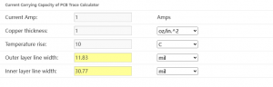
                      PCB Copper Thickness Calculator

                      ToolFeaturesBest For
                      Saturn PCB Toolkit• IPC-2152 compliant
                      • Auto-derating
                      • Impedance modeling
                      Power electronics
                      EEWeb Online Calculator• Temperature rise graphs
                      • Exportable reports
                      • Mobile-friendly
                      Quick field checks
                      Altium Integrated Tool• Real-time DRC
                      • Multi-layer analysis
                      • 3D thermal simulation
                      Altium users

                      Welcome to contact EBest Circuit (Best Technology) if you need to calculate PCB copper thickness: sales@bestpcbs.com.

                      You may also like

                      Polyimide PCB Manufacturer in China, Over 18 Years

                      July 21st, 2025

                      Why choose polyimide PCB?ā€Œ This guide details their critical properties, thickness, thermal conductivity, pros and cons, manufacturing processes and applications.

                      Are you still troubled by these problems?

                      • Complex circuit design leads to low yield?
                      • Traditional materials degrade in humid environment?
                      • Does micro-aperture processing affect circuit accuracy?

                      EBest Circuit (Best Technology) äøØPolyimide PCB Manufacturer in China Over 18 years:

                      • High-precision graphic transfer technology: using laser direct imaging (LDI) process, line width/line spacing up to 25μm, yield increased by 30%.
                      • Ultra-low water absorption material: 0.2% water absorption formula, insulation resistance retention rate in humid environment> 95%.
                      • Precision micro-hole processing: CO2 laser + UV laser combined drilling, aperture accuracy ±15μm, hole wall roughness <10μm.

                      Welcome to contact us if you have any request for polyimide PCB: sales@bestpcbs.com.

                      What Is Polyimide PCB?

                      A polyimide PCB is a flexible printed circuit board utilizing polyimide as its dielectric substrate, providing remarkable flexibility for repeated bending, folding, or twisting without mechanical damage. This polymer offers exceptional thermal stability, handling temperatures up to 400°C, a low dielectric constant near 3.5, and high tensile strength, making it suitable for electronics requiring dynamic movement or intricate three-dimensional packaging.

                      Commonly applied in neural implants and wearable devices, these PCBs enable reliable electrical connections in space-constrained environments while maintaining performance under stress. Fabrication involves microelectronics-compatible techniques, supporting mass production for high-density interconnects across medical and consumer applications.

                      What Is Polyimide PCB?

                      How Thick Is a Polyimide PCB?

                      Core Material Thickness

                      • Base Polyimide Filmā€Œ: Typically ā€Œ12.5 μm to 100 μm (0.0005–0.004 inches)ā€Œ, with ā€Œ25 μm (0.001 inch)ā€Œ and ā€Œ50 μm (0.002 inches)ā€Œ being industry standards.
                      Total Stackup Thickness

                      • Single-Layer Flexible PCBā€Œ: ā€Œ50–125 μm (0.002–0.005 inches)ā€Œ when combined with copper foil (9–18 μm).
                      • ā€ŒMulti-Layer Designsā€Œ: Ranges ā€Œup to 0.3 mm (0.012 inches)ā€Œ for 4–6 layer configurations using adhesive bonding.

                      Influencing Factors

                      • Copper Foilā€Œ: Ultra-thin ā€Œ9–18 μmā€Œ electrodeposited copper reduces bulk.
                      • ā€ŒAdhesive Layersā€Œ: Bonding films add ā€Œ10–25 μmā€Œ per layer; adhesive-less laminates reduce total thickness to ā€Œ30 μmā€Œ.
                      • ā€ŒStiffenersā€Œ: Localized PI or steel reinforcements (ā€Œ0.1–0.3 mmā€Œ) enhance connector zones.
                      Polyimide PCB Material Data Sheet & Properties

                      Property CategoryTest ParameterTest StandardValue with UnitCharacteristics
                      Physical PropertiesDensityASTM D7921.43 g/cm³Lightweight design advantage
                      Water AbsorptionASTM D5700.3%Low moisture absorption for high-frequency stability
                      Flammability RatingUL94Non-flammableComplies with aerospace safety requirements
                      Mechanical PropertiesTensile StrengthASTM D63890 MPa3Ɨ stronger than FR-4 substrates
                      Elongation at BreakASTM D6386-8%High ductility for dynamic bending applications
                      Flexural StrengthASTM D79098 MPaSupports 5mm bend radius designs
                      Thermal PropertiesHDT @1.82MPaASTM D648360ā„ƒWithstands reflow soldering
                      Continuous Operating Temp.UL746B260ā„ƒSuitable for automotive electronics
                      CTE (Z-axis)ASTM D6961-5Ɨ10⁻⁵ /ā„ƒMatches copper foil expansion (Cu: 17Ɨ10⁻⁶/ā„ƒ)
                      Electrical PropertiesDk @1MHzIEC 602503.4 Low signal loss for high-frequency transmission
                      Volume ResistivityIEC 6009310¹⁷ Ω·cm100Ɨ higher insulation than standard materials
                      Dielectric StrengthIEC 60243110-120 kV/mmSuperior high-voltage breakdown resistance
                      Special PerformanceFlex Life @5mm radiusIPC-6013D>100,000 cyclesValidated in smart wearable devices
                      Peel Strength (Cu foil)IPC-TM-650≄1.0 N/mmEnsures flex circuit reliability
                      Min. Line Width/SpacingIPC-222330/30 μmUltra-high-density routing capability

                      What Is the Thermal Conductivity of Polyimide Flex PCB?

                      Material TypeThermal ConductivityEnhancement Mechanism
                      Pure Polyimide (PI)0.18 W/(mĀ·K)N/A (base material)
                      PI/CNNS Nanocomposite2.04 W/(mĀ·K) (+1033%)CNNS in-plane self-orientation
                      Graphene-PI CompositeUp to 739.56 W/(mĀ·K)Layered graphene thermal networks

                      What Are the Pros and Cons of Polyimide Circuit Board?

                      Pros (Advantages)ā€Œ

                      • High wiring density and miniaturizationā€Œ: Enables compact designs for space-constrained applications like mobile devices or wearables.
                      • Lightweight and thin profileā€Œ: Reduces overall weight and thickness of electronic products, ideal for portable electronics.
                      • Excellent flexibility and durabilityā€Œ: Can withstand millions of dynamic bends without wire breakage, supporting complex 3D assemblies.
                      • Versatility in spatial layoutā€Œ: Allows arbitrary scaling and movement in three-dimensional space for integrated component connections.
                      • Broad applicabilityā€Œ: Suitable for high-reliability fields such as aerospace, military, and digital cameras due to robust insulating properties.

                      Cons (Disadvantages)ā€Œ

                      • High initial costā€Œ: Design, routing, and photographic processes are expensive due to specialized manufacturing requirements.
                      • Limited use for general applicationsā€Œ: Typically justified only for specific needs, not cost-effective for standard PCBs.
                      • Maintenance challengesā€Œ: Repair and rework, such as soldering, require trained personnel to avoid damage.
                      What Are the Pros and Cons of Polyimide Circuit Board?

                      What Are Applications of Flexible Polyimide PCB?

                      Applications of Flexible Polyimide PCB

                      • Consumer Electronics – Foldable displays (smartphones/tablets).
                      • Aerospace – High-temperature wiring in satellites/spacecraft.
                      • Medical Devices – Wearable sensors (ECG patches/implantable modules).
                      • Automotive – Battery management systems (EVs) & autonomous vehicle sensors.
                      • Industrial Automation – Flexible joints in robotic arms/motion control systems.
                      • Energy – Solar panel interconnections (flexible photovoltaic modules).
                      • Telecommunications – High-frequency signal routing in 5G/mmWave devices.
                      What Are Applications of Flexible Polyimide PCB?

                      How Are Polyimide PCBs Manufactured?

                      Manufacturing Process of Flexible Polyimide PCBs

                      1. Material Preparation

                      • Base Film: Polyimide (PI) film (12.5–50µm) selected for thermal stability (Tg > 250°C).
                      • Adhesive Coating: Epoxy/acrylic adhesive applied to PI film for copper bonding.

                      2. Copper Cladding

                      • Lamination: Adhesive-coated PI film laminated with electrolytic copper foil (1/3–2 oz) at 180–200°C.
                      • Temporary Carrier: Aluminum/steel carrier attached for ultra-thin FPCs to prevent warping.

                      3. Circuit Patterning

                      • Dry Film Application: Photosensitive dry film laminated onto copper.
                      • Exposure & Development: UV light exposes circuit pattern; unexposed areas washed away.
                      • Etching: Ferric chloride/alkaline etching removes unprotected copper (line width/spacing ≄25µm).

                      4. Coverlay Application

                      • PI Coverlay: Second PI film with adhesive laminated over circuits for protection.
                      • Laser Ablation: COā‚‚ laser drills precision holes (via/pad openings).

                      5. Plating & Surface Finish

                      • ENIG Plating: Electroless nickel/immersion gold applied to pads for solderability.
                      • Stiffener Bonding: FR4/PI stiffeners attached to connector zones via thermal bonding.

                      6. Testing & Inspection

                      • AOI: Automated optical inspection for defects (open/short circuits).
                      • Electrical Testing: Flying probe/bed-of-nails tests verify continuity/impedance.

                      7. Cutting & Forming

                      • Laser Cutting: Precision shaping of FPC outlines.
                      • Bending Test: Flexibility validation (1,000+ bend cycles at 180°).

                      8. Final Cleaning & Drying

                      • Ultrasonic Cleaning: Removes residual particles from etching/plating.
                      • Baking: FPCs dried in 80–100°C oven to eliminate moisture.

                      9. Packaging

                      • Anti-Static Protection: FPCs placed in anti-static bags with desiccant packs.
                      • Cushioning: Foam inserts or vacuum-formed trays used to prevent movement.
                      • Labeling: Barcode/QR code labels include product ID, batch number, and RoHS compliance.

                      10. Quality Final Check

                      • Visual Inspection: Confirm no scratches, folds, or contamination.
                      • Electrical Recheck: Sample testing for critical parameters (e.g., impedance).
                      How Are Polyimide PCBs Manufactured?

                      Polyimide PCB Manufacturer in China – EBest Circuit (Best Technology)

                      Reasons why choose us as polyimide PCB manufacturer:

                      • 24-hour rapid prototyping: shorten the R&D cycle by 50% and accelerate product launch.
                      • 1 Piece MOQ: zero inventory risk, trial production cost reduced by 90%.
                      • Competitive & Transparent Pricing – No hidden costs, offering the best value without compromising quality.
                      • Turnkey Solutions – Full-service PCB manufacturing from design to delivery, accelerating your product’s time-to-market.
                      • ISO 14001/ISO 13485 certification: medical/automotive customers are exempt from secondary testing, and compliance costs are reduced by 30%
                      • 0.075mm ultra-thin substrate processing: folding screen FPC thickness is reduced by 40%, and the bending life reaches 200,000 times.
                      • Mature blind and buried via technology: circuit density increased by 40%, adapting to the needs of 5G modules/medical implants.
                      • Free DFM (Design for Manufacturability) Analysis: Optimizes PCB layouts to reduce material waste, lower production costs, and avoid late-stage design revisions.

                      Please feel free to contact EBest Circuit (Best Technology) if you have any inquiry for polyimide PCB: sales@bestpcbs.com. Looking forward to hearing from you soon!

                      You may also like

                      Superb Quality PCB Contract Manufacturing for High-mix Needs

                      July 21st, 2025

                      PCB contract manufacturing plays a key role in today’s electronics industry, especially during prototyping. It bridges the gap between design and actual production, helping teams launch new hardware faster and with fewer mistakes. If you’re struggling with design flaws, delays, or inconsistent quality, you’re not alone. Many companies face the same issues—and that’s where a reliable PCB partner becomes a game-changer.

                      At EBest Circuit (Best Technology), our prospects and regular customers get superb quality PCB contract manufacturing from Prototypes to PCBA. Providing superb quality, high mix, fast delivery, and no MOQ turnkey PCB assembly to an increasingly competitive market is our market positioning. You can enjoy our technical capability for customizing a variety of PCBs, such as single-sided PCBs, multilayer PCBs, HDI PCBs, extra-thin PCBs, high-speed PCBs, and so on. If you have any inquiries regarding PCB fabrication services or PCBA contract manufacturing, just shoot us an email at sales@bestpcbs.com.

                      What is PCB Contracting?

                      PCB contracting refers to a collaborative business model where a company outsources the production and assembly of printed circuit boards to a professional third-party under a contractual framework. It typically encompasses both PCB contract manufacturing—focused on fabrication and assembly execution—and engineering collaboration, such as DFM (Design for Manufacturability) optimization and material selection consulting. While the terms are often used interchangeably, PCB contracting emphasizes the strategic partnership aspect, whereas contract manufacturing focuses on process delivery.

                      In a typical setup, the client submits finalized design files—like Gerber, BOM, and ODB++—and the contractor takes over fabrication, component sourcing, assembly (including SMT, through-hole, or hybrid), functional testing, and even certification compliance (such as RoHS, REACH, or UL).

                      This model is increasingly adopted across high-demand sectors such as automotive electronics, aerospace systems, 5G communication infrastructure, AI computing platforms, and industrial automation. The reason is simple: it reduces internal overhead, enhances speed-to-market, and provides immediate access to advanced capabilities without investing in in-house facilities.

                      With the right PCB contract partner, companies benefit from much more than just manufacturing—they gain co-engineering insight, proactive design validation, and a scalable supply chain that accelerates product launch while minimizing risk.

                      What is PCB Contracting?

                      Does PCB Assembler Provide Services from Prototype to PCBA?

                      Yes. A capable PCB assembler usually provides support from prototyping to full PCBA. EBest Circuit (Best Technology), for example, offers design reviews, prototyping, component sourcing, fabrication, PCBA, and testing, streamlining every step. Our early collaboration tools and strict DFM reduce common prototype failures like thermal blind spots and impedance errors.

                      What Does PCB Fabrication Services Include?

                      PCB fabrication services cover everything needed to produce bare boards. This includes material selection, layer stack-up planning, copper etching, drilling vias, solder mask application, and surface finishing. Quality fabricators like EBest Circuit (Best Technology) go further by offering impedance control, zero-void microvias, and warpage control to avoid delamination and BGA defects in prototypes.

                      How to Ensure Quality During PCBA Contract Manufacturing?

                      Ensuring quality during PCBA contract manufacturing requires a combination of advanced inspection tools, robust process control, and traceable component sourcing. At EBest Circuit (Best Technology), we integrate a multi-stage quality management protocol aligned with industry best practices:

                      1. Incoming Inspection
                        Our quality process begins at the gate. In addition to XRF spectroscopy for verifying metal content in surface finishes (such as ENIG or immersion silver), we conduct visual inspections, dimensional checks, and dielectric resistance validation on laminate materials. This ensures compliance with IPC-4101 and IPC-6012 standards before production even starts.
                      2. In-Process Control
                        During SMT and through-hole assembly, we utilize 3D AOI (Automated Optical Inspection) paired with cutting-edge defect recognition software. While our internal defect detection rate is over 99.7%, we still apply manual review stations at critical checkpoints. This hybrid approach helps catch subtle issues such as tombstoning, skewed components, and incomplete solder joints, which automated systems alone may miss.
                      3. Final Testing & Validation
                        Before delivery, every board undergoes comprehensive testing based on its design class. These include:
                        • TDR (Time Domain Reflectometry): For impedance validation in high-speed circuits.
                        • Thermal Shock Testing: Simulates environmental stress across -40°C to +125°C cycles.
                        • ICT (In-Circuit Test): Detects shorts, opens, and passive value deviations.
                        • FCT (Functional Circuit Test): Verifies logic performance and power integrity under load.
                      4. Component Integrity & Traceability
                        To counter component substitution—especially during global shortages—we implement a dual-layer approach:
                        • Vendor Qualification: We source only from authorized distributors with RoHS/REACH-compliant declarations.
                        • Blockchain-Linked BOM Tracking: A secure digital ledger ties each part to its supplier, batch number, and inspection record. This safeguards against counterfeit components and ensures end-to-end traceability.

                      Our closed-loop SPC (Statistical Process Control) system continuously monitors process deviations and initiates AI-driven corrections in real-time. Through this ecosystem, we’ve reduced prototype-related defects by up to 78%, helping customers meet tight timelines without sacrificing reliability.

                      Is Turnkey PCB Assembly Difficult?

                      Not with the right partner. Turnkey PCB assembly means the contractor handles fabrication, sourcing, assembly, and testing. It may sound complex, but EBest Circuit (Best Technology) simplifies it using integrated systems. Their Component Bank Network provides common stocked items, reducing sourcing delays. We also use a three-shift production model for faster delivery—most prototypes ship in 5 days.

                      Is Turnkey PCB Assembly Difficult?

                      Why Might a Company Choose PCB Contract Manufacturing?

                      There are many reasons companies prefer contract manufacturing:

                      • Cost Efficiency: Avoids large capital investment in manufacturing facilities.
                      • Speed: Speeds up prototype iterations and reduces launch delays.
                      • Expertise: Gains access to experienced engineers and technicians.
                      • Risk Reduction: Minimizes design-induced and process-based errors.

                      Ultimately, outsourcing enables companies to focus on design innovation while specialists like EBest Circuit (Best Technology) take care of the rest.

                      Why Choose EBest Circuit (Best Technology) for PCB Contract Manufacturing?

                      EBest Circuit (Best Technology) goes far beyond just assembling boards. Our strengths are rooted in solving the most common and costly customer needs during prototyping. Here’s how they lead the market:

                      • Design-Manufacturability Support: Our advanced DFM tools and early collaboration portal catch thermal gaps, impedance issues, and unclear markings before production.
                      • Advanced Manufacturing: From 20-layer HDI with tight impedance control to surface prep, we support even complex builds.
                      • High-mix PCB lines: Our PCB portfolio includes FR4, semi rigid-flex PCB, FPC, MCPCB, ceramic PCB. All PCBs support the full service from PCB prototypes to SMT PCBA.
                      • End-to-End Traceability: MES integration gives full transparency and trust.
                      • Speed: With 3-shift lines and additive hybrid processes, lead times drop by up to 85%.
                      • Certifications: AS9100D, ISO 13485, and IATF 16949 ensure compliance across critical sectors.
                      Why Choose EBest Circuit (Best Technology) for PCB Contract Manufacturing?

                      Prototyping is not just about quick builds—it’s about building it right the first time. PCB contract manufacturing can either simplify or complicate your workflow depending on the partner you choose. EBest Circuit (Best Technology) helps eliminate 78% of common prototype issues by combining engineering collaboration, certified manufacturing, and lightning-fast production. From 1-layer boards to aerospace-grade 20-layer stacks, we’re more than just a supplier—we’re a co-engineering partner. If you have any questions or need any help, please contact us via email at sales@bestpcbs.com.

                      You may also like

                      Better Quality Aluminium PCB Manufacturer for Prototype

                      July 18th, 2025

                      Aluminium PCB manufacturerĀ plays a critical role in delivering high-performance prototypes for power-dense applications like LED lighting, automotive electronics, and industrial controls. When speed and reliability matter, choosing the right partner makes all the difference.

                      EBest Circuit (Best Technology) is an aluminium PCB manufacturer in China, supplying better quality aluminium PCB from prototypes to mass manufacturing services in a rapidly growing market. Our factory is fully compatible with ISO 9001, ISO 13485, IATF 16949, AS9100D, UL, REACH, and RoHS. No matter whether you need aluminum PCB board, copper PCB board, China IMS PCB, or custom MCPCB, we have a full product line for your selection. PleaseĀ emailĀ us with your Gerber files or any suggestions at sales@bestpcbs.com. We would be delighted to give you our quote and the viable solutions.

                      Better Quality Aluminium PCB Manufacturer for Prototype

                      What is the Difference Between Aluminum PCB and FR-4?

                      Aluminum PCB vs FR4 is one of the most common decisions in circuit design—especially when thermal performance matters. FR-4 is a standard fiberglass-reinforced epoxy material with good electrical insulation and mechanical strength. It’s affordable, easy to process, and ideal for most general-purpose electronics. However, its thermal conductivity is quite low, typically around 0.3 W/mK.

                      In contrast, aluminum PCBs use a metal base—usually 5052 or 6061 aluminum alloy—paired with a thermally conductive dielectric. Their thermal conductivity ranges from 5 to 10 W/mK, allowing them to transfer heat much faster than FR-4. This makes aluminum PCBs the better choice for high-power LED lighting, power converters, automotive modules, and motor drivers where heat buildup can affect performance or cause failure.

                      • When to Use Aluminum PCBs?

                      Use aluminum when your design includes high-current components, dense LED arrays, or thermal hotspots that demand effective heat dissipation. They’re also beneficial in compact enclosures where airflow is limited.

                      • When to Use FR-4?

                      Choose FR-4 for cost-sensitive designs, lower power circuits, or consumer electronics that don’t produce much heat. It’s more flexible in terms of stackup and supports multi-layer routing better.

                      • Why Choose Aluminum Over FR-4?

                      Aluminum PCBs protect temperature-sensitive components by lowering the junction temperature. This improves reliability, reduces thermal stress, and extends the product’s lifespan. So, when thermal performance is a key concern, aluminum is a smarter choice than FR-4.

                      What is the Difference Between Aluminum PCB and FR-4?

                      Who Are the Biggest Aluminium PCB Manufacturers in China?

                      China is a major hub for aluminium PCB manufacturing. Here are three top companies you should know:

                      1. EBest Circuit (Best Technology): Known for quality and precision, EBest Circuit (Best Technology) provides aluminium PCBs with tight tolerances and fast delivery.
                      2. Suntak Technology: A large volume manufacturer offering mass production services and affordable pricing for general applications.
                      3. JLCPCB: Popular for online orders and low-cost prototyping. While fast, the tradeoff may be limited customization.

                      In conclusion, if you’re seeking a balance between quality and speed, EBest Circuit (Best Technology) offers advanced control for rapid prototyping while ensuring fewer errors.

                      Who is the Largest PCB Aluminium LED Manufacturer in North America?

                      North America has several key players in LED aluminium PCB production. Here are three leading manufacturers:

                      1. Advanced Circuits: Based in Colorado, they specialize in prototype-to-volume PCB builds with quick turnaround and LED capabilities.
                      2. Sunstone Circuits: Offers aluminium core solutions for LED applications with a focus on customer support and design assistance.
                      3. Rush PCB Inc.: Known for fast lead times and complex stackups for high-brightness LED products.

                      These manufacturers cater to diverse industry needs, from commercial lighting to automotive and industrial applications, leveraging aluminum PCBs’ superior thermal management properties. Their services typically include design validation, rapid prototyping, and volume production with certifications like UL and ISO compliance.

                      Who Are Aluminium PCB Manufacturers in India?

                      India’s aluminium PCB market is growing steadily. Below are three reliable manufacturers:

                      1. Shogini Technoarts: Based in Pune, they provide both single and double-sided aluminium PCBs with thermal vias.
                      2. Circuit Systems India: Located in Gandhinagar, offering advanced prototyping and quick delivery.
                      3. Fine-Line Circuits Ltd.: Mumbai-based, experienced in export and specialized PCBs for lighting and industrial sectors.

                      Overall, Indian suppliers offer affordable solutions, though delivery timelines can be longer. Choose based on your volume and lead time needs.

                      Who Are Aluminium PCB Manufacturers in India?

                      What is the Aluminium PCB Manufacturing Process?

                      1. Raw Material Preparation:Ā Selection of aluminium base material and defining the copper foil thickness depending on the design’s power needs.
                      2. Aluminium Surface Treatment:Ā The aluminium base undergoes chemical oxidation or passivation to improve bonding strength with the dielectric layer.
                      3. Lamination:Ā High-pressure and high-temperature lamination process bonds the copper foil, dielectric layer, and aluminium base firmly. This stage is critical, as poor bonding causes delamination.
                      4. Image Transfer:Ā Circuit pattern is created using dry film photoresist, UV exposure, and development to define the copper traces.
                      5. Etching:Ā Unwanted copper is removed using etchants such as ferric chloride or cupric chloride to form the circuit pattern.
                      6. Drilling:Ā Special carbide or diamond-coated tools are used to drill through high-hardness aluminium with high precision.
                      7. Plating:Ā Via holes are electroplated with copper or nickel to improve conductivity and ensure strong interconnection.
                      8. Solder Mask:Ā Applied via screen printing or spray, then exposed and developed to protect copper traces. Most aluminium PCBs use white solder mask with black silkscreen for better LED light reflection. Black solder mask with white silkscreen is used for decorative or display lighting, offering better contrast.
                      9. Surface Finish:Ā OSP, HASL, or ENIG is applied depending on component requirements. OSP suits flat pads for SMT. HASL is common for through-hole assembly. ENIG is ideal for fine-pitch ICs.
                      10. Profiling:Ā CNC or V-cut machines shape the board. CNC depth control is especially critical for cavity designs in LED arrays.
                      11. Inspection:Ā AOI and X-ray machines are used to verify solder quality and detect internal defects like voids or bridging.

                      Some challenging stages include lamination (risk of delamination), surface treatment (poor bonding), and CNC profiling (cavity depth tolerance within ±0.01mm). EBest Circuit (Best Technology) optimizes these with real-time thermal simulation, high-speed CNC, and MES-based quality tracking for better consistency.

                      Why Use Aluminium PCB Board for LED?

                      LEDs generate significant heat during operation. Aluminium PCBs help dissipate this heat efficiently, protecting both the light output and the lifespan of the LEDs. Compared to standard FR-4 boards, an aluminium PCB board for LED can typically reduce the junction temperature by around 15°C to 30°C, depending on factors like copper thickness, thermal structure, and ambient conditions. This enhanced thermal performance improves the long-term reliability of LEDs, especially in demanding applications like automotive lighting and streetlamps.

                      What is the Most Costliest PCB?

                      The most costly PCBs are those that combine high layer counts with advanced fabrication processes. Multi-layer boards with 16 layers or more—especially up to 32 layers—are at the top end due to their complex lamination, precise drilling, and intricate interconnections. These boards often require multiple press cycles and tight registration, significantly increasing production time and cost.

                      HDI PCBs (High-Density Interconnect) also fall into the premium category, especially Type III HDI structures. These use laser-drilled microvias, stacked vias, and via-in-pad designs. The fabrication complexity and yield challenges can push their cost 180% to 200% higher than standard multilayer boards.

                      Aluminum core PCBs, though cost-effective in handling heat for power applications, are inherently more expensive than traditional FR-4 boards due to the metal substrate. When designers add thermal vias, copper coin inserts, or heat-sink cavities, the manufacturing process becomes more demanding—further raising costs.

                      Another major cost driver is embedded component technology, where passive or active elements are integrated directly into the board. This technique requires special materials like ABF (Ajinomoto Build-up Film) and precision layering. The result is a thinner and more compact product, but with a substantial cost increase.

                      In Summary, while aluminum boards with advanced thermal designs can be expensive, 32-layer multilayer PCBs and advanced HDI PCBs represent the highest cost segment due to their demanding processing and tight tolerances. Embedded component PCBs also contribute to the top-tier pricing because of the material and manufacturing complexity involved.

                      How to Choose Aluminium PCB Manufacturers in China?

                      Look for the following when selecting a partner:

                      1. Certifications (IPC, RoHS, UL, IATF16949).
                      2. Experience with aluminium substrates and thermal design.
                      3. In-house testing: AOI, thermal cycling, X-ray.
                      4. Fast lead times without sacrificing quality.
                      5. MES system for traceability and defect tracking.

                      EBest Circuit (Best Technology) ticks all the above boxes and goes beyond with engineering support to solve failure-prone designs.

                      Why Choose EBest Circuit (Best Technology) as Your Trustworthy Aluminium PCB Manufacturer?

                      EBest Circuit (Best Technology) stands out as a dependable aluminium PCB manufacturer by addressing customers’ needs directly:

                      1. Reducing Technical Failures:Ā AOI and X-ray inspections stop solder bridging. Low-CTE dielectrics prevent warpage. Optimized lamination cuts delamination risk.
                      2. Better Thermal Management:Ā Plugged copper vias and aluminium substrates dissipate heat fast. ANSYS-based thermal simulation avoids hotspots.
                      3. Certified Assurance:Ā IPC Class III, ISO 9001, ISO 13485, IATF 16949, and AS9100D ensure lower field failures. Every board meets RoHS and UL standards.
                      4. Rapid Lead Time: 48-hour precision machining with ±0.01mm tolerance and sequential lamination means no trade-off between speed and complexity.
                      5. One-stop manufacturing service: Our factory provides services from prototype to assembly. Whether you need 1 PCS prototype or 1,000,000 PCS MCPCB SMT PCBA, we can support you fully with rapid lead time.

                      Unlike other aluminium PCB board manufacturers, EBest Circuit (Best Technology) offers solutions, not excuses. We help customers avoid costly rework by controlling each detail from design to delivery. This makes our aluminium PCB SMT manufacturing trusted by global brands in lighting, automotive, and industrial sectors.

                      Why Choose EBest Circuit (Best Technology) as Your Trustworthy Aluminium PCB Manufacturer?

                      So, if you are tired of sourcing from unreliable aluminium PCB manufacturers in China or facing repeated failures in your LED boards, it’s time to consider EBest Circuit (Best Technology)—where speed, reliability, and care meet in every prototype we deliver. Please feel free to email us at sales@bestpcbs.com if you have any questions or would like a quote.

                      You may also like

                      Electronic Component Failure Analysis: Why it occurs?

                      July 18th, 2025

                      What Is Electronic Component Failure?

                      When any part inside an electronic system stops working as expected, it’s called an electronic component failure. This could mean a capacitor no longer holds charge, a resistor burns out, or an integrated circuit malfunctions. Even one small faulty component can lead to major issues in the final product.

                      To find out why a component failed, engineers use a process called electronic component failure analysis. This process involves inspecting the part visually and electrically, identifying how and why the fault happened, and using that information to avoid similar problems in the future. It’s essential for quality assurance, product reliability, and cost control in any electronics-related business.

                      Electronic Component Failure Analysis

                      Types of Electronic Component Failure

                      Electronic components can fail in different ways depending on the stress they endure. Below are the four most common types:

                      1. Mechanical Failure

                      Mechanical failure happens when there is a physical breakdown of the component’s structure. Some failures are often caused by vibration, improper handling, or dropping a device. In mobile or automotive electronics, this type of failure is especially common due to frequent movement. Common typical failures are including:

                      • Cracked solder joints
                      • Broken leads or pins
                      • Fractured PCB substrates
                      • Loose connectors due to vibration

                      You might notice components that are no longer connected properly to the board or parts that move when touched. Visual inspection often reveals cracks or loosened parts caused by physical force.

                      2. Thermal Failure

                      All electronic parts generate some heat when they operate. However, if the heat is not controlled properly, components can overheat and become damaged. This is known as thermal failure.

                      For example, semiconductors like transistors and integrated circuits are sensitive to high temperatures. When they get too hot, their internal structure may break down, leading to permanent damage.

                      3. Aging Failure

                      Components have a natural lifespan. Over time, materials degrade, and the component can no longer perform its function correctly. This is called aging failure.

                      Electrolytic capacitors are well-known for this issue—they tend to dry out after years of use, causing them to lose their ability to hold charge. Similarly, solder joints can crack after repeated heating and cooling cycles (called thermal cycling), leading to poor connections.  In addition to this, typical aging failures also including:

                      • Metal fatigue in solder joints
                      • Battery capacity reduction
                      • Deteriorated dielectric layers

                      4. Packaging Failure

                      Electronic components are enclosed in packaging to protect the inner materials. If the packaging is flawed or gets damaged during use, it may expose the component to moisture, dust, or chemicals.

                      For instance, water vapor may seep through a cracked chip case and cause corrosion inside. This is especially risky in humid or corrosive environments. Packaging failure is often seen as cracking, blistering, or delamination of the part’s outer shell.

                      Types of Electronic Component Failure

                      Causes of Electronic Component Failure

                      To solve problems effectively, it’s important to understand the root causes behind failures. Below are the most common causes engineers encounter during electronic component failure analysis:

                      1. Overvoltage and Overcurrent

                      Every electronic component has a maximum voltage and current rating. Exceeding these limits can damage the internal structure, often leading to immediate failure. For example, sending too much current through a resistor can cause it to overheat and burn. Applying excessive voltage to a capacitor can cause it to explode or leak.

                      2. Poor Soldering or Manufacturing Defects

                      Faulty assembly techniques can lead to short circuits, intermittent connections, or component movement. Cold solder joints—where the solder didn’t melt completely—can crack over time.

                      If a component is misaligned or not soldered properly to all its pads, it may not function or may fail under mechanical stress. These defects are usually caught through visual inspection or X-ray analysis.

                      3. Electrostatic Discharge (ESD)

                      Static electricity may not hurt humans, but it can destroy sensitive components like MOSFETs and ICs instantly. Even a small ESD event can damage internal junctions, creating invisible faults that show up later during use.

                      4. Environmental Stress

                      Moisture, dust, salt, or chemicals in the air can corrode metal parts, especially in outdoor or industrial environments. Extreme temperatures or frequent thermal cycling can stress materials, causing them to crack or delaminate.

                      5. Inadequate Design or Component Selection

                      Using the wrong part for the job—such as a low-voltage capacitor in a high-voltage section—can lead to early failure. Similarly, ignoring derating rules (operating parts near their limit) can reduce lifespan dramatically.

                      How to Check Faulty Electronic Components?

                      When a device isn’t working, checking the components one by one is a logical step. Here’s how to do that effectively:

                      1. Visual Inspection

                      The first step is always to look carefully. Use a magnifying glass or microscope if needed. There are some signs can be checked directly if components get failure. Look for:

                      • Burn marks or discoloration
                      • Cracks or broken legs
                      • Bulging or leaking capacitors
                      • Lifted or cracked solder joints
                      • Warping or melting

                      2. Smell

                      Burnt electronic parts release a strong smell. If a section of the board smells like burnt plastic or metal, you’re probably close to the damaged part.

                      3. Touch Test (with Caution)

                      Once the power is OFF and the board is safe to handle, you can gently feel components. If one feels much hotter than the rest, it may be failing. Never touch live circuits, and use caution even when power is removed—capacitors may still hold a charge.

                      4. Comparison Method

                      If you have an identical working device, compare it with the faulty one. Swapping parts one by one can help isolate which component isn’t working.

                      5. Multimeter Testing

                      A digital multimeter is your best tool. You can test for open circuits, shorts, or measure resistance, voltage, and continuity. We’ll explain this in the next section in detail.

                      How to Prevent Electronic Component Failures?

                      While you can’t prevent all failures, many of them can be avoided with good design, handling, and maintenance practices.

                      • Always source your components from reputable suppliers. Cheap or counterfeit parts are far more likely to fail.
                      • Avoid pushing components near their max voltage, current, or temperature limits.
                      • Add surge protection (like TVS diodes or fuses) where needed.
                      • Use appropriate PCB layout techniques for signal integrity and thermal control.
                      • Use anti-static wrist straps and mats when handling sensitive parts.
                      • Store components in anti-static bags or boxes.
                      • Avoid touching component pins directly.
                      • Good soldering practices and correct part orientation go a long way. Automated optical inspection (AOI) and in-circuit testing (ICT) help ensure quality during production.
                      • For circuits exposed to moisture or dust, apply conformal coating or potting material to prevent corrosion and shorts. Use enclosures with proper IP ratings if the device will be outdoors.
                      • Use heatsinks, thermal vias, fans, or thermal pads to keep parts cool. High temperatures shorten component life more than almost any other factor.

                      How to Test Electronic Components with a Multimeter?

                      A multimeter is one of the most useful tools for checking components, it can be tested various parts, here is how to test:

                      How to Test Electronic Components with a Multimeter?

                      1. Testing Capacitors

                      • Discharge the capacitor before testing.
                      • Set the multimeter to capacitance mode (if available).
                      • Connect probes to the leads.

                      A large difference between the reading and rated value suggests aging or failure.

                      Note: If your multimeter lacks capacitance mode, you can test for short or open conditions using resistance mode.

                      2. Testing Diodes and LEDs

                      • Set the meter to diode test mode.
                      • Connect the red probe to the anode and the black to the cathode.
                      • A good diode should show a forward voltage drop (~0.6–0.7V).
                      • Reversing the probes should show no reading.

                      LEDs can also be tested this way, and a faint light may even flash when tested in forward bias.

                      3. Testing Transistors

                      Bipolar junction transistors (BJTs) can be tested by checking base-emitter and base-collector junctions like diodes.

                      • Use diode mode.
                      • Test base-to-emitter and base-to-collector—each should show ~0.6V in forward bias.
                      • Reversed probes or collector-to-emitter should show no conduction.
                      • If you get readings in all directions, the transistor may be shorted.

                      4. Testing ICs

                      Integrated circuits are difficult to test with just a multimeter. You usually need to power the board and check input/output signals or use dedicated IC testers.

                      FAQs

                      1. What is the first sign of electronic component failure?

                      Burn marks, strange smells, or malfunctioning behavior are common early signs of component issues.

                      2. How do you test an electronic component without removing it from the circuit?

                      You can test many components in-circuit using a multimeter, but readings may be affected by parallel components.

                      3. How often should electronics be inspected for aging components?

                      Critical systems should be checked annually, while consumer devices may only need service after several years.

                      4. What is the role of derating in preventing failures?

                      Derating means operating components below their maximum limits to reduce stress and increase reliability.

                      5. Can failure analysis improve future product design?

                      Yes, analyzing failed parts helps engineers refine design, choose better materials, and improve overall durability.

                      If you’re working on a repair or want to improve your product’s reliability, proper electronic component failure analysis is a valuable step. Want help with failure diagnostics or reliable PCB assembly? Reach out to EBest Circuit (Best Technology) — your trusted partner for high-quality, certified PCB and PCBA solutions.

                      We follow strict quality control with quality control systems, and offer full traceability for manufacturing, report, datasheet… If you want to do PCB assembly or components sourcing, welcome to reach us at sales@bestpcbs.com.

                      You may also like