For a USB 2.0 High-Speed port, start with a low-capacitance ESD diode close to the connector. Route D+ and D− past the protection pads without long branches, and give the diode a short return into the intended reference. Verify both USB signal quality and system ESD behavior: a board can enumerate and still reset during a discharge, or survive a strike and still fail the High-Speed eye test.
usb 2.0 esd protection
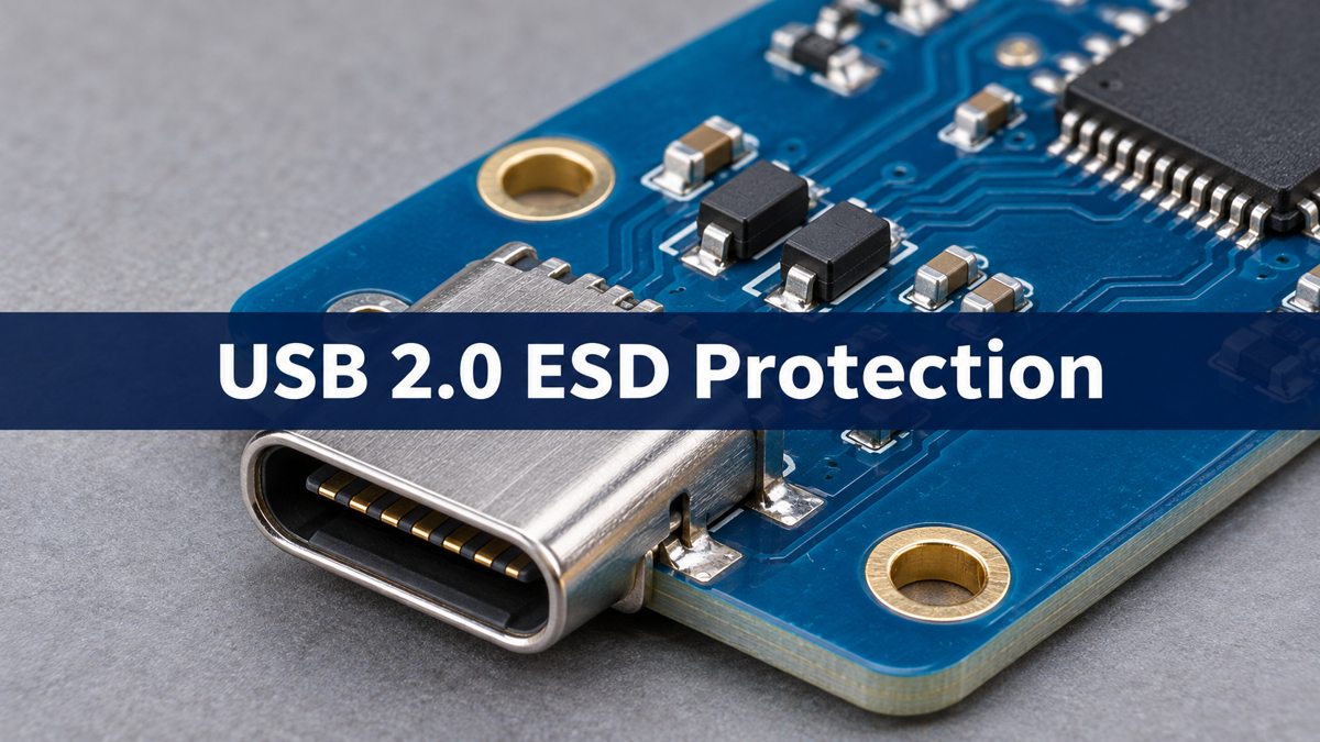
Protect the path from the exposed connector to the USB transceiver. When a transient exceeds the diode’s operating region, the diode conducts current into its return path instead of allowing all of the pulse to continue toward the transceiver. During normal signaling the device should remain off, but its capacitance still loads the pair. The goal is to minimize both the discharge loop and the disturbance seen by the data signals.
usb esd protection circuit
Draw two paths before choosing the footprint: the D+/D− signal path from the connector to the PHY, and the transient current path from each exposed data line through its protector into the designated return. The reference circuit for the selected part determines which pin is the return and whether the device uses a rail reference. A D+/D− protector does not establish protection for VBUS, CC or SuperSpeed pairs. For the rest of the interface, see the USB-C PCB design guide.
usb 2.0 esd protection diode
Choose a device against the PHY and connector requirements, not the largest advertised discharge rating. For example, TI’s USB application note lists ESD122 as a dual-channel D+/D− option with a 3.6 V reverse working voltage and 0.2 pF listed capacitance. Those figures belong to that device; use its current datasheet for test conditions and limits, then check actual layout and system behavior.
| Parameter | Decision check |
| Working voltage, V | Check against normal line voltage |
| Line capacitance, pF | Use stated test conditions and PHY budget |
| Clamping voltage, V | Compare only at matching pulse conditions |
| Channel and package | Confirm pin map and a routable return |
| Discharge rating, kV | Check method; verify on the complete product |
esd diode placement
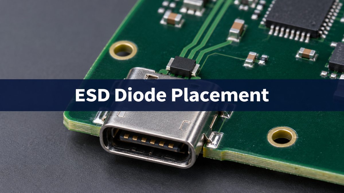
Put the protector at the first practical point after the connector and keep both the connection to the data pads and the discharge return short. A component can look close in the placement view while its ground trace makes a long trip around a cutout. Check the copper layers and return vias, not just the component outline. Do not route the unprotected connector segment alongside sensitive circuitry if it can be avoided.
usb esd protection layout
Prefer flow-through routing when the part and footprint allow the data traces to pass directly through the protection-pad area. The diode remains a shunt element; the name describes the routing, not a series electrical connection. A short branch can be an alternative if the pinout forces it and the implemented design passes both signal and system ESD tests.
| Routing option | Use and trade-off |
| Flow-through | First choice when pad map and return align |
| Very short branch | Possible when constrained; measure the result |
| Long branch or remote clamp | Revise: extra stub and transient loop |
usb differential pair routing
Keep the two data paths physically similar through the connector, protector and first layer transition. Review reference continuity and avoid adding a long test stub to only one member of the pair. In a hypothetical compact service-port board that resets during cable-side testing, first inspect the discharge route and nearby reset or power circuits. If the same board also shows poor High-Speed signaling, check the diode capacitance, pad discontinuities and pair asymmetry before choosing a different clamp rating.
usb 2.0 differential impedance
The usual High-Speed differential routing target is 90 Ω nominal; confirm the tolerance and stackup requirements for the design. A calculated trace width covers the uniform section, not the pad and via transitions. Review those transitions separately, and include the protection device’s capacitance. The relevant data rate is 480 Mbit/s in High-Speed mode, but edge behavior is not determined by the bit rate alone.
usb 2.0 eye diagram
After a layout revision, verify the applicable High-Speed electrical test separately from the system ESD test. Use the specified USB test mode and fixture for the electrical test; for ESD, record the strike point, polarity, operating mode and allowed recovery behavior under the product test plan. Monitor real data traffic, resets and re-enumeration. Release only when the electrical result meets its applicable limits and the product meets its own ESD performance criterion. Successful charging or idle enumeration is not a substitute for either check.
FAQ
Can one array cover VBUS and the two data lines?
Some products can, but check the channel specifications and routing. VBUS operating voltage and exposure may differ from the data lines.
Is a larger TVS diode always a safer upgrade?
No. A larger part may add capacitance or create a worse return path. Check clamp behavior under comparable pulse conditions as well as link quality.
Can I place the protector on the bottom side?
Sometimes. Compare the complete path including signal vias, return vias and loop geometry. Verify the actual implementation rather than judging it by distance in a top view.
Should the common-mode choke go before the diode?
In TI’s TUSB121x example it follows the ESD protection. Confirm the sequence in the PHY and protector references and qualify it on the actual board.
Does a connector shield replace the data-line protector?
No. Shield bonding and signal-line protection address different paths. Follow the intended chassis and board grounding architecture rather than assuming they are interchangeable.
Why might the port restart even though no diode failed?
A transient can disturb the supply, reset path or reference. Capture the symptom and investigate the current route and nearby sensitive circuits before replacing the diode. The PCB ground bounce guide explains how a changing local reference can show up in a measurement.
Is a device-level rating proof of system compliance?
No. The assembled product adds connector, enclosure, layout and grounding variables. Verify it with the applicable system test and performance criteria.
Does this placement apply unchanged to USB SuperSpeed?
No. Check the separate transmit and receive paths, channel budget and AC coupling architecture. This guide addresses USB 2.0 D+ and D−.
Sources
Texas Instruments: ESD and Surge Protection for USB Interfaces; Texas Instruments: TUSB121x board guidelines; Nexperia: ESD protection for USB 2.0 interfaces.
Project Review
For a PCB fabrication discussion, send Best Technology the proposed stackup, pair geometry and connector-to-protector region at sales@bestpcbs.com.
You may also like

Tags: Differential Routing, esd protection, Signal Integrity, USB 2.0