Add a USB 2.0 common mode choke only if the evidence points to noise on the data pair and the part improves emissions without consuming too much High-Speed signal margin. Compare a populated choke and a qualified bypass under the same test conditions. If emissions improve but the eye fails, the choke is not ready for production.
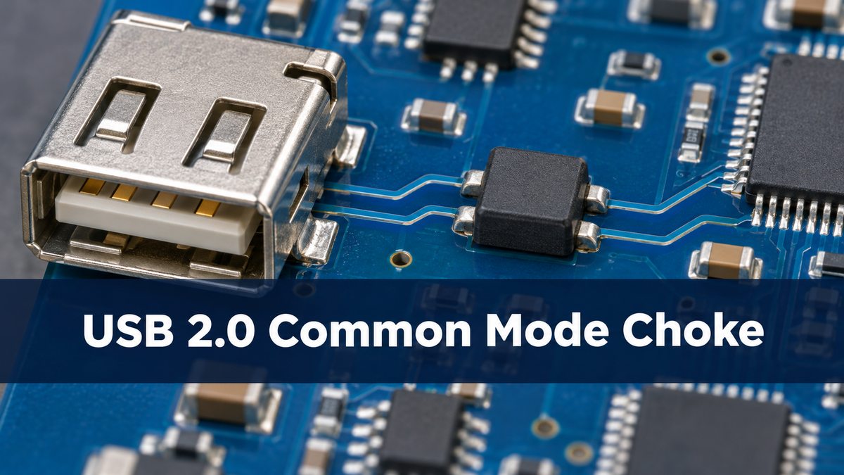
usb 2.0 common mode choke
A two-line choke uses coupled windings in series with D+ and D−. Ideally, signals flowing in opposite directions see little added impedance, while noise flowing in the same direction on both lines sees more. Real devices also have parasitics and differential loss. The part does not replace ESD protection, nor does it establish the pair’s PCB impedance.
usb common mode noise
First decide which path is carrying the noise. In a hypothetical USB service port, a radiated peak appears only when the cable is attached. That makes the cable a useful clue, not proof that D+ and D− are the source. Compare activity with controlled traffic and examine the shield and power paths. A data-pair choke will not necessarily address noise predominantly carried on VBUS or the shield.
common mode choke impedance
Read common-mode impedance versus frequency, then check the differential transmission and balance data. For example, Murata lists 90 Ω ±25% at 100 MHz for DLW21SN900SQ2 under its specified test conditions. That number is common-mode impedance at one frequency; it is not a differential routing target, bandwidth, or guarantee of attenuation in the product.
| Parameter | What to compare |
| Common-mode impedance, Ω | Curve around the suspect frequency |
| Differential loss, dB | Curve across the relevant signal band |
| DC resistance, Ω | Maximum and balance between lines |
| Package and pinout | Channel mapping and footprint |
usb common mode choke selection
Prefer a device with relevant mixed-mode data and enough signal margin in the implemented layout. A higher catalog impedance at one frequency can still be the wrong choice if loss or imbalance increases. Keep a qualified bypass option where practical, but do not assume a jumper footprint is electrically invisible. Compare the routing geometry and inspect the built boards.
usb common mode choke placement
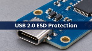
Follow the actual PHY and protection guidance. TI’s TUSB121x example places the choke close to the receptacle, on the PHY side of the ESD devices. That is a named implementation, not a universal placement rule. Preserve the shortest protection path from the connector and review the two parts together. See the USB 2.0 ESD placement guide for the separate transient-path check.
usb differential pair routing
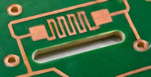
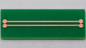
Keep the pair symmetric through the connector, protector, choke pads and layer changes. If you provide bypass footprints, avoid an unused branch hanging from only one line. A common-mode problem can be aggravated by imbalance in the routing, so compare both the footprint and the continuous reference before asking the choke to hide a layout problem.
usb 2.0 radiated emissions
Compare the two builds using the same cable, orientation, equipment arrangement and representative activity. In the example, suppose the suspect peak falls by 4 dB after fitting the choke. That is an illustrative comparison, not a lab result or a compliance claim. Confirm the absolute result against the project’s applicable limit and check repeatability before crediting the component.
| Outcome | Decision |
| Emissions and eye both meet limits | Confirm repeatability before release |
| Emissions improve but eye fails | Reject; revisit part or routing |
| Eye passes but emissions do not improve | Trace the actual noise path |
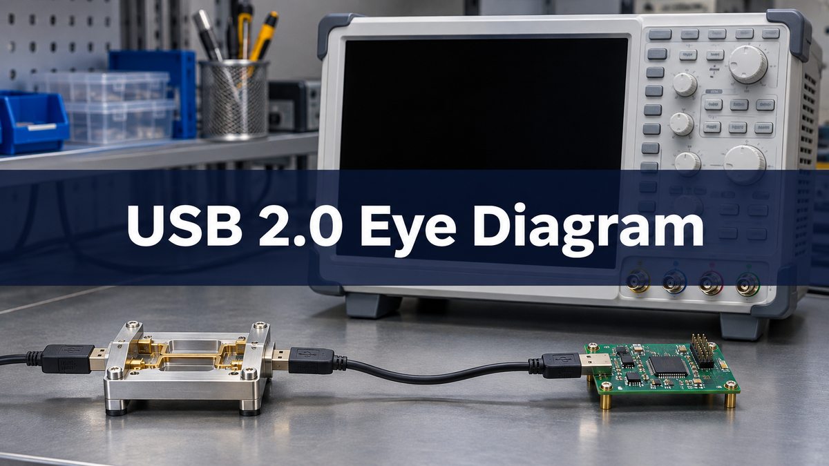
usb 2.0 eye diagram
Verify the 480 Mbit/s High-Speed eye in the applicable test mode and fixture, not just enumeration or a short file transfer. A tight result with one cable is a reason to repeat the approved test under the required conditions, not to declare the change safe. For the controller example, release the choke only after the emissions result and the applicable USB electrical result both meet the agreed criteria.
FAQ
Is the choke needed on every High-Speed port?
No. Use evidence from the intended system and the device guidance. A correctly working port need not add unnecessary loading.
Can I select a choke using only its 100 MHz impedance?
No. Compare frequency-dependent common-mode behavior, differential loss and the actual board measurements.
Can a bypass trial leave the pads empty?
Not if that opens the signal lines. Use the qualified bypass connection for the designed footprint.
Does enumeration show the High-Speed eye passes?
No. Enumeration is a functional observation. Use the applicable electrical test for the eye and signal limits.
Will the choke fix ESD resets?
Not by default. Inspect the discharge path and protection design separately, then verify the system’s ESD behavior.
Should I compare different cables in the first A/B test?
Keep the cable fixed for the first comparison. Test additional required cables separately to verify system robustness.
Can a data-pair choke fix VBUS noise?
Only if the coupling path involves the data pair and the change is shown to help. Inspect the power path if that is the dominant source.
Does a lower measured peak mean the product is compliant?
No. Check the applicable limit, modes and repeatability. A relative improvement and a compliance result are different claims.
Sources
TI TUSB121x board guidelines; TDK: USB 2.0 EMC practice; Murata DLW21SN specifications.
Project Review
For a Best Technology fabrication discussion, send the stackup, D+/D− geometry, connector footprint and choke or bypass options to sales@bestpcbs.com.
You may also like

Tags: Common Mode Choke, EMI Testing, Signal Integrity, USB 2.0