





A high voltage PCB has to do more than carry a higher electrical potential. Its layout, insulation system, laminate, conductor geometry, surface condition, and manufacturing tolerances all influence whether the finished board can operate safely without arcing, surface tracking, insulation breakdown, or premature field failure.
EBest Circuit supports high-voltage PCB fabrication and PCBA projects from prototype through production. For projects involving special insulation spacing, heavy copper, controlled dielectric thickness, isolation slots, or unusual stack-ups, send your Gerber files, stack-up, operating voltage, peak voltage, material requirements, and application information to sales@bestpcbs.com for an engineering review and quotation.
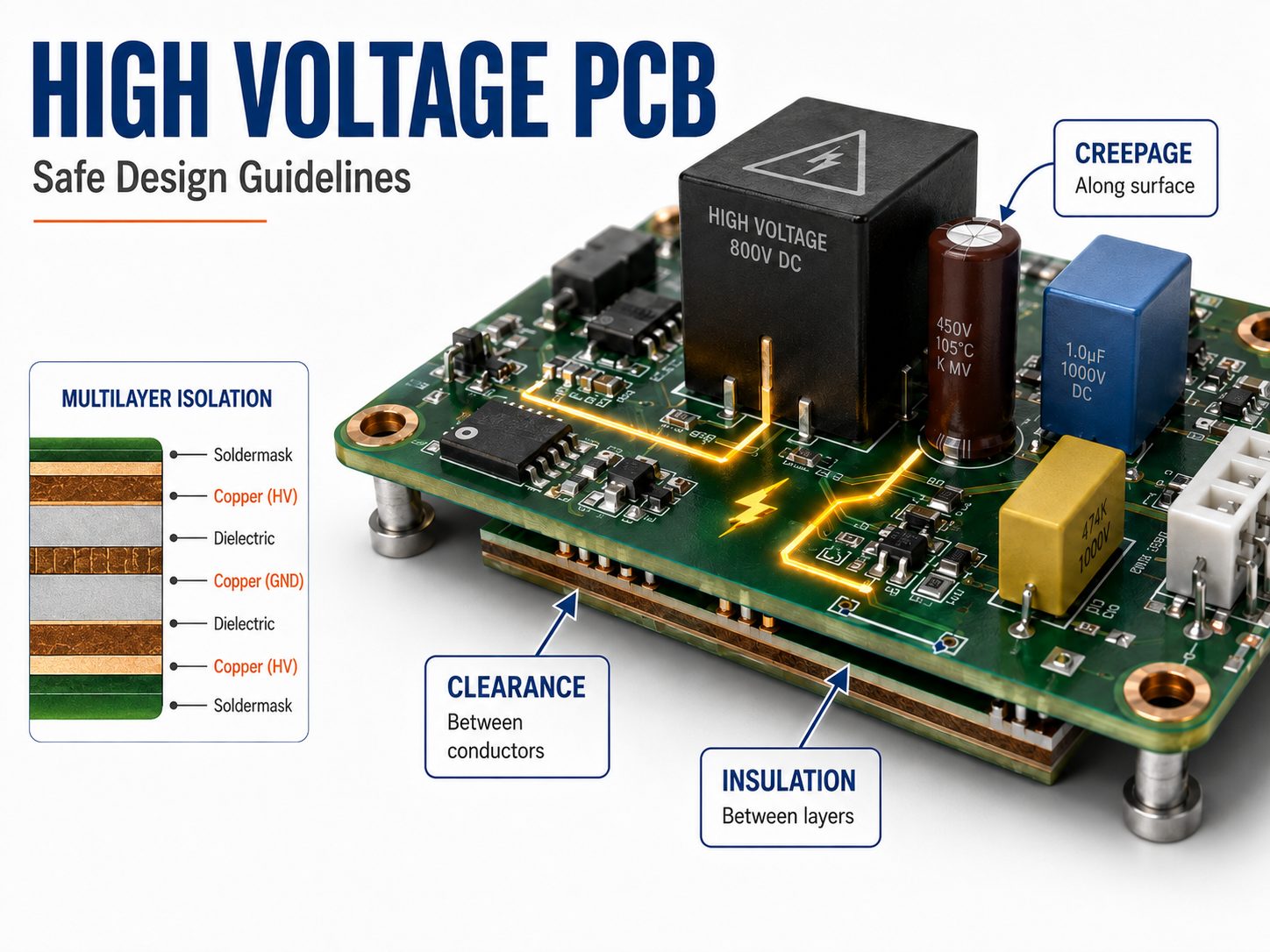
What Is a High Voltage PCB?
A high voltage PCB is a circuit board designed with additional insulation, spacing, material, and layout controls to safely handle elevated voltage differences between conductors.
There is no single PCB-industry voltage threshold above which every circuit automatically becomes a high-voltage PCB. In practical power-electronics work, approximately 300 V to 1,000 V is a useful range where high-voltage spacing and insulation considerations become increasingly important, while properly engineered boards can operate above 1 kV.
Typical applications include:
- EV charging and battery systems
- Industrial power supplies
- Solar inverters
- Motor drives
- High-voltage test equipment
- Medical electronics
- Power conversion equipment
- Energy storage systems
- High-voltage measurement circuits
The key distinction is therefore not simply the number printed beside the voltage rail. A reliable design has to manage insulation coordination across traces, pads, layers, component leads, PCB edges, slots, coatings, and the surrounding environment.
How Much Voltage Can a PCB Handle?
For practical high-voltage PCB design, working voltages around 300–1,000 V are common design territory, while specially engineered PCBs can operate above 1 kV; there is no universal maximum PCB voltage rating.
The actual limit is usually determined by the weakest insulation path rather than by the FR-4 laminate alone.
For example, a laminate may have high dielectric strength while an assembled PCB still fails because two exposed pads are too close, contamination forms a conductive surface path, or an unexpected surge exceeds the designed clearance.
Voltage capability is influenced by:
- Working voltage: continuous or repetitive voltage between conductors
- Peak voltage: maximum DC or AC peak potential difference
- Transient voltage: switching spikes and surge events
- Clearance: shortest air path between conductive parts
- Creepage: shortest surface path between conductive parts
- Dielectric thickness: insulation between PCB layers
- Material CTI: resistance to surface tracking
- Altitude: lower air pressure reduces air insulation capability
- Pollution and moisture: contamination can reduce surface resistance
For design and RFQ purposes, it is therefore more useful to specify working voltage + peak/transient voltage than to state only “1,000 V PCB.”
What Is the Difference Between Creepage and Clearance in High Voltage PCB Design?
Clearance is the shortest distance through air between two conductive parts, while creepage is the shortest distance along an insulating surface.
| Parameter | What It Measures | Main Failure Risk |
| Clearance | Shortest path through air | Arcing / air breakdown |
| Creepage | Shortest path along an insulating surface | Surface tracking |
| Solid insulation | Path through dielectric material | Dielectric breakdown |
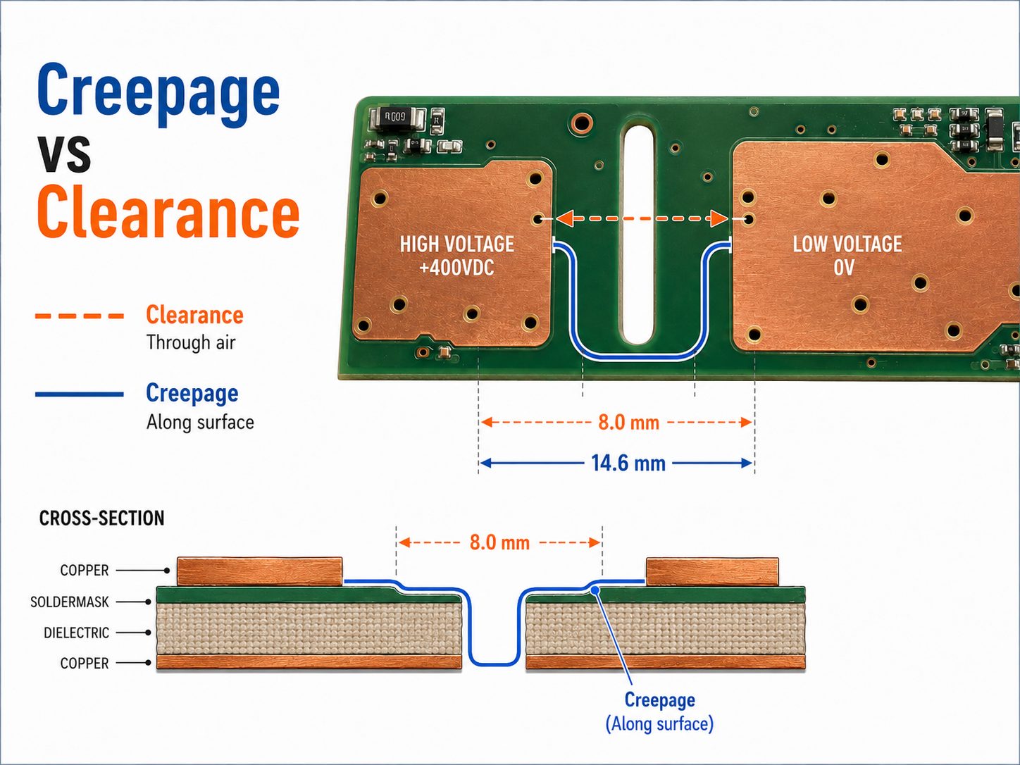
Suppose two high-voltage pads are separated by a routed slot. The slot can substantially lengthen the surface path and therefore increase creepage, but the shortest air path must still be checked separately for clearance.
This distinction matters because the two distances are determined differently. Clearance is strongly influenced by transient voltage and altitude, while creepage depends heavily on working voltage, pollution degree, and the CTI of the insulating material.
How Do You Determine High Voltage PCB Clearance and Creepage?
As a practical example, at 400 V RMS, IEC 60664-1 gives a creepage reference of about 2.0 mm for Pollution Degree 2 and Material Group I, but the requirement increases to about 4.0 mm for Material Group III.
That difference is why voltage alone cannot determine the final spacing.
Typical IEC 60664-1 creepage references for Pollution Degree 2 are:
| Working Voltage | Material Group I | Material Group II | Material Group III |
| 400 V RMS | 2.0 mm | 2.8 mm | 4.0 mm |
| 800 V RMS | 4.0 mm | 5.6 mm | 8.0 mm |
| 1,000 V RMS | 5.0 mm | 7.1 mm | 10.0 mm |
These values illustrate how strongly material tracking performance can affect creepage.
The design sequence should be:
- Determine the actual working voltage.
- Identify the maximum transient or impulse voltage.
- Define whether the insulation is functional, basic, supplementary, or reinforced.
- Determine the pollution degree.
- Check the laminate CTI and material group.
- Account for operating altitude.
- Apply the requirements of the relevant end-product standard.
Clearance follows a different calculation path.
For example, typical IEC 60664-1 basic-insulation clearance values at up to approximately 2,000 m include:
| Required Impulse Voltage | Typical Minimum Clearance |
| 0.5 kV | 0.2 mm |
| 1.5 kV | 0.5 mm |
| 2.5 kV | 1.5 mm |
| 4.0 kV | 3.0 mm |
| 6.0 kV | 5.5 mm |
This demonstrates why a 400 V circuit cannot automatically be assigned “a 400 V clearance.” Its required clearance may instead be controlled by a 2.5 kV, 4 kV, or higher impulse requirement.
What High Voltage PCB Trace Spacing Should You Use?
For external uncoated conductors, a useful PCB design reference is approximately 1.25 mm at 151–300 V peak and 2.5 mm at 301–500 V peak; at 1,000 V, the spacing reaches about 5.0 mm under the familiar IPC external-uncoated conductor rule.
A practical reference table is:
| Voltage Difference, DC or AC Peak | External Uncoated Conductor Spacing |
| 31–150 V | 0.60 mm |
| 151–300 V | 1.25 mm |
| 301–500 V | 2.50 mm |
| 600 V | ≈3.0 mm |
| 800 V | ≈4.0 mm |
| 1,000 V | ≈5.0 mm |
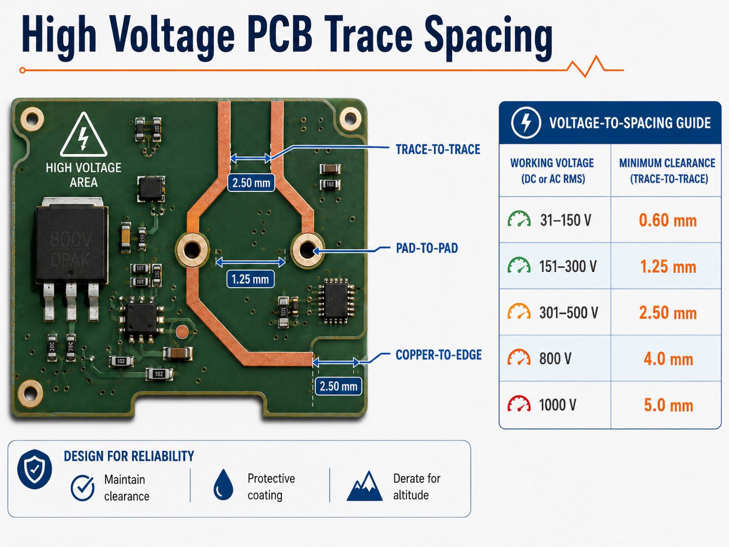
For values above 500 V, the external-uncoated reference increases by approximately 0.005 mm per volt above 500 V.
For example:
1,000 V: 2.5 mm + (500 × 0.005 mm) = 5.0 mm
IPC-2221C is the current IPC-2221 revision. It retains conductor-spacing categories while refining areas such as altitude, vacuum operation, and coating definitions, so the current standard should be checked when establishing released design rules.
These PCB conductor-spacing values should not be treated as the final safety clearance for every product. Medical, mains-powered, industrial, automotive, or reinforced-insulation designs may require greater spacing under their applicable IEC or UL safety standard.
Designers should also check more than trace-to-trace spacing:
- trace to pad
- pad to pad
- copper to board edge
- trace to mounting hole
- trace to chassis
- copper to exposed component lead
- high-voltage to low-voltage plane
- outer-layer to inner-layer conductor
The correct design value is the minimum finished-board distance after manufacturing tolerance, not merely the nominal CAD spacing.
Which Materials Are Best for a High Voltage PCB?
High-CTI FR-4 is suitable for many high-voltage PCBs, while specialized high-voltage laminates become more attractive when surface tracking, humidity, thermal stress, or insulation reliability is more demanding.
The most important properties include:
| Material Property | Why It Matters |
| CTI | Resistance to conductive surface tracking |
| Dielectric strength | Resistance to breakdown through insulation |
| Moisture resistance | Helps preserve insulation in humid environments |
| CAF resistance | Reduces conductive filament reliability risk |
| Tg | Influences thermal dimensional stability |
| Td | Indicates thermal decomposition behavior |
| Resin system | Affects insulation and processing behavior |
| Z-axis stability | Important for multilayer reliability |
CTI is not the same as dielectric strength.
Dielectric strength concerns breakdown through the insulating material.
CTI evaluates resistance to conductive tracking across its surface.
This is why two FR-4 materials with similar dielectric strength can require different creepage distances when their CTI classifications differ.
For demanding designs, specifying only “FR-4” is therefore insufficient. The RFQ should identify either the laminate grade or the required CTI, thermal, flammability, and insulation properties.
How Should You Plan the Stack-Up for a High Voltage PCB?
A high-voltage stack-up should first separate HV and low-voltage domains with controlled dielectric thickness, rather than simply adding layers around an existing layout.
The exact dielectric thickness cannot be reduced to one universal number because it depends on the required solid-insulation voltage withstand, laminate system, insulation class, and applicable product standard.
The stack-up should define:
- dielectric thickness between high-voltage layers
- high-voltage-to-low-voltage layer separation
- copper thickness
- material dielectric properties
- resin content
- finished board thickness
- internal plane clearances
- via structures crossing voltage domains
Internal copper is surrounded by solid dielectric, so its insulation mechanism differs from exposed surface copper.
Avoid placing a low-voltage or grounded plane immediately underneath a high-voltage node unless the vertical insulation path has been intentionally evaluated.
High-current high-voltage designs need another check. Increasing copper weight can reduce conductor resistance, but heavier copper also changes etching capability, conductor spacing, resin fill, dielectric construction, and finished board thickness.
For unusual HV constructions, stack-up review should therefore happen before final routing, not after the Gerber files are complete.
What Are the Key High Voltage PCB Layout Guidelines?
The most effective layout rule is to create clearly separated HV and LV zones and maintain the required isolation distance around the complete boundary on every copper layer.
Useful layout practices include:
- Separate HV and SELV/low-voltage areas.
- Maintain the isolation boundary on every copper layer.
- Avoid sharp copper points in high-electric-field regions.
- Use smooth trace and copper transitions where practical.
- Keep HV copper away from uncontrolled PCB edges.
- Include vias and plated holes when checking spacing.
- Avoid unnecessary test points inside HV areas.
- Keep contamination-sensitive regions accessible for cleaning.
- Check component body and lead spacing.
- Prevent copper pours from entering isolation gaps.
A common design error is creating a large visible clearance on the top layer while an internal copper plane extends underneath the same isolation barrier.
Another occurs around components. The traces may meet the intended rule while transformer pins, connector contacts, heat sinks, screws, or component leads create a shorter path.
A high-voltage layout review should therefore inspect the finished electrical assembly, not only individual traces.
When Should You Use Isolation Slots, Barriers, or Conformal Coating?
Use an isolation slot when PCB area is limited and additional creepage is needed; use barriers when the physical insulation path needs to be extended; use conformal coating mainly when environmental contamination or moisture must be controlled.
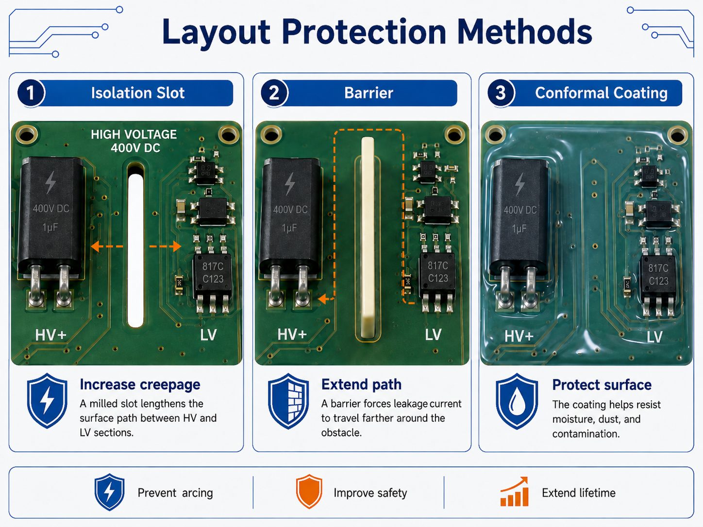
These three methods solve different problems.
Isolation slots interrupt the direct PCB surface path and can significantly increase creepage without requiring the same increase in board width.
Barriers physically extend or separate insulation paths and may also help prevent contamination from bridging conductive regions.
Conformal coating protects the PCB from humidity, dust, chemicals, and surface contamination.
Coating performance depends on:
- coating material
- thickness
- adhesion
- coverage
- cure quality
- pinholes
- component shadowing
- operating environment
- applicable standard
Do not assume that ordinary solder mask or conformal coating automatically allows a safety clearance to be reduced.
If an isolation slot is safety-critical, specify its finished minimum width, position, and tolerance on the manufacturing documentation rather than relying only on nominal CAD geometry.
Which Standards Apply to High Voltage PCB Design?
For general PCB design, IPC-2221C is a key reference; for insulation coordination, IEC 60664-1 is one of the most important standards, while the final equipment standard determines the binding safety requirement.
| Standard | Typical Relevance |
| IPC-2221C | Generic printed board design and conductor spacing |
| IEC 60664-1 | Clearance, creepage, insulation coordination |
| IEC 62368-1 | AV and ICT equipment |
| IEC 60601-1 | Medical electrical equipment |
| UL 796 | Printed wiring boards |
| Product-specific IEC/UL standards | Final equipment safety requirements |
The key point is that an IPC spacing table does not automatically prove product safety compliance.
A medical device, EV charger, industrial controller, mains power supply, or ICT product may require different insulation levels even if their PCB operating voltages appear similar.
What Manufacturing Factors Matter for High Voltage PCBs?
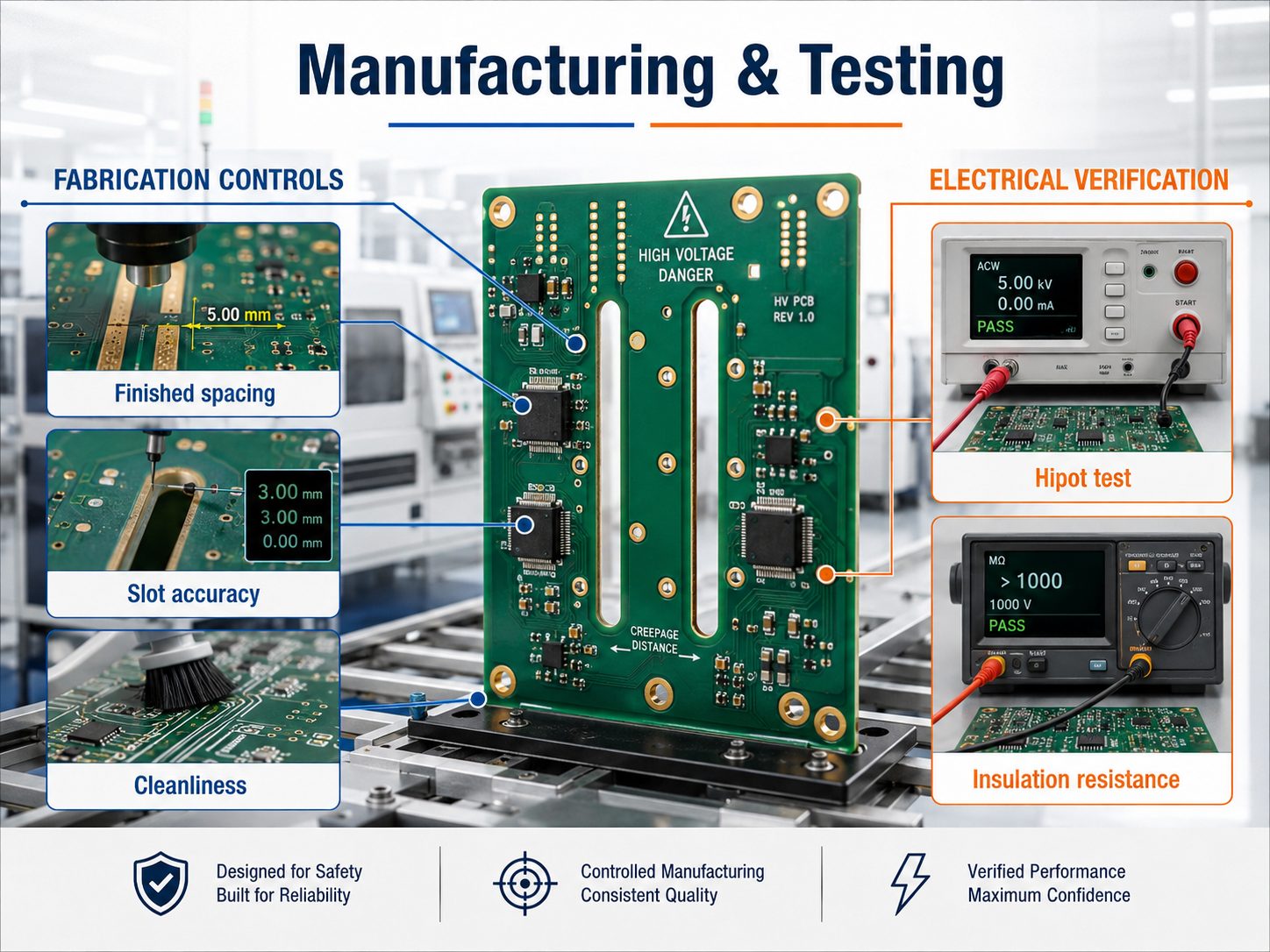
The most critical manufacturing requirement is that the finished PCB must preserve the minimum insulation distances assumed by the designer after etching, drilling, routing, lamination, and registration tolerances are included.
Key controls include:
- Copper geometry: etching must not reduce critical spacing.
- Copper-to-edge distance: routing tolerance must be included.
- Isolation slots: finished dimensions must meet the required minimum.
- Dielectric thickness: critical insulation layers must match the approved stack-up.
- Material control: laminate substitutions require engineering review.
- Surface cleanliness: ionic contamination can weaken surface insulation.
- Solder mask registration: misalignment may expose copper.
- Routing and drilling accuracy: holes and slots can alter creepage paths.
- Lamination quality: voids and delamination are undesirable in stressed dielectric structures.
- Traceability: safety-related products may require controlled material and process records.
For example, if a design requires a 2.50 mm finished minimum conductor spacing, drawing two features exactly 2.50 mm apart in CAD leaves no manufacturing tolerance.
This is why high-voltage fabrication notes should clearly distinguish between the nominal design dimension and the minimum finished-board requirement. That distinction helps ensure normal fabrication tolerances do not reduce critical spacing below the required minimum.
How Should a High Voltage PCB Be Tested?
At minimum, a high-voltage PCB should receive normal open/short electrical testing; projects with safety-related insulation commonly add insulation-resistance and dielectric-withstand, or hipot, testing according to the product specification.
Depending on the application, verification may include:
- open/short electrical test
- insulation resistance test
- dielectric withstand / hipot test
- dimensional inspection of isolation gaps
- isolation-slot inspection
- cleanliness testing
- conformal-coating inspection
- functional testing at operating voltage
- first-article validation
A hipot test applies a specified voltage between isolated regions and checks whether the insulation can withstand that electrical stress without unacceptable leakage or breakdown.
There is no responsible universal rule such as:
“Test every 1,000 V PCB at 2,000 V.”
The correct hipot voltage and duration come from the end-product standard or approved test specification.
The test document should define:
- test voltage
- AC or DC
- duration
- ramp rate
- leakage-current limit
- test points
- pass/fail criteria
For assembled boards, PCB-only testing may not be enough. Connectors, component leads, heat sinks, screws, cables, and other hardware can create shorter insulation paths than the bare board itself.
What High Voltage PCB Design Mistakes Should You Avoid?
The most common high-voltage PCB mistake is choosing spacing from nominal operating voltage alone instead of evaluating peak voltage, creepage, clearance, environment, and manufacturing tolerance together.
Other common problems include:
- Confusing clearance with creepage. Increasing the surface path does not automatically increase the air path.
- Ignoring altitude. Above approximately 2,000 m, IEC insulation calculations may require clearance correction.
- Selecting laminate only by dielectric strength. CTI, moisture resistance, thermal behavior, and contamination also matter.
- Assuming solder mask provides reinforced insulation. This depends on the construction and applicable safety standard.
- Ignoring internal copper. An outer-layer isolation zone can still contain a hidden plane violation.
- Leaving sharp copper features in HV regions. Sharp geometry can increase local electric-field concentration.
- Checking PCB traces but not components. Leads, terminals, heat sinks, connectors, and hardware must also maintain isolation.
- Designing exactly to the minimum spacing. Fabrication tolerances must be added before design release.
A useful high-voltage design review question is therefore:
Does the finished and assembled product maintain the required insulation under its actual voltage, transient, altitude, contamination, manufacturing tolerance, and service conditions?
FAQs About High Voltage PCB
What voltage is considered high voltage on a PCB?
There is no universal PCB threshold, but approximately 300 V and above is a useful practical point at which clearance, creepage, transients, insulation, and environmental conditions deserve explicit review. Designs in the 300–1,000 V range are common high-voltage PCB territory, while boards above 1 kV are feasible with appropriate engineering.
How much clearance does a high voltage PCB need?
For external uncoated PCB conductors, a useful IPC reference is about 1.25 mm for 151–300 V peak and 2.50 mm for 301–500 V peak, increasing to approximately 5.0 mm at 1,000 V under the external-conductor rule. Product-safety requirements can require larger values.
What is the difference between creepage and clearance?
Clearance is the shortest path through air, while creepage is the shortest path along an insulating surface.
Is FR-4 suitable for high voltage PCBs?
Yes. High-CTI FR-4 is suitable for many 300–1,000 V-class PCB applications, provided its CTI, dielectric construction, thermal performance, creepage, clearance, and end-product requirements are appropriate.
Does conformal coating increase voltage isolation?
It can improve environmental protection and surface insulation performance, but it does not automatically justify smaller safety spacing. The coating material, coverage, process qualification, and applicable standard must support the reduction.
How does altitude affect PCB clearance?
Clearance normally increases with altitude because air density decreases. Above approximately 2,000 m, the applicable standard may require an altitude correction factor.
Can isolation slots increase creepage distance?
Yes. A correctly placed slot can substantially increase creepage without requiring the same increase in PCB width, although clearance must still be checked separately.
If you are developing a high-voltage PCB and want the fabrication capability checked before prototype release, send your Gerber files, stack-up, working voltage, peak or surge voltage, copper weight, material requirements, critical isolation dimensions, and applicable standard to sales@bestpcbs.com. EBest Circuit can review stack-up manufacturability, critical spacing, isolation slots, copper geometry, dielectric construction, and other fabrication-sensitive features before quotation and production.
You may also like



Tags: high voltage pcb, high voltage PCB clearance, High Voltage PCB Design, high voltage PCB design guidelines, high voltage PCB trace spacing