PCB manufacturing PCB manufacturing
Home > Blog

ceramic pcb board

Ceramic PCB for Power Devices: Materials, Design, and Procurement Guide
Friday, June 5th, 2026

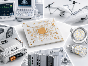
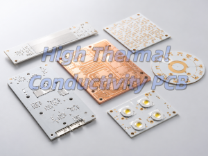
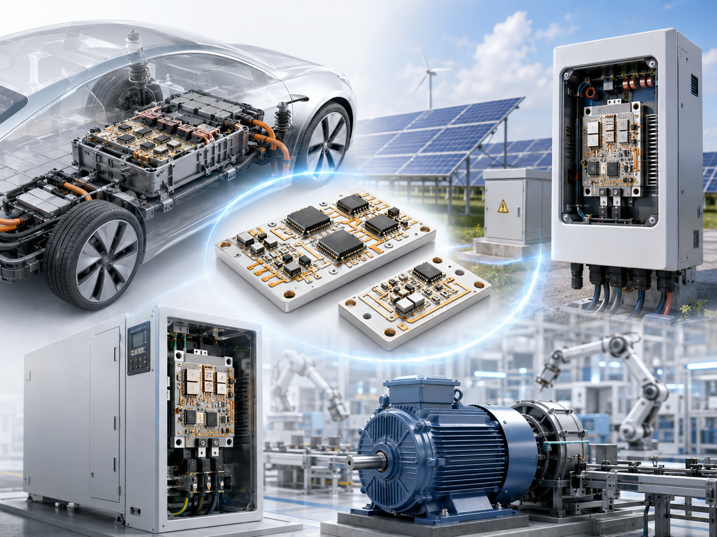
Power devices generate heat, carry high current, and often operate under voltage stress. A standard FR4 PCB can work well in many electronic products, but power modules, SiC devices, GaN devices, IGBT modules, MOSFET packages, rectifiers, high-power LEDs, solar inverters, EV systems, and industrial drives often need stronger thermal paths and better electrical insulation. This is where a ceramic PCB becomes valuable.

Ceramic PCB for Power Devices: Materials, Design, and Procurement Guide

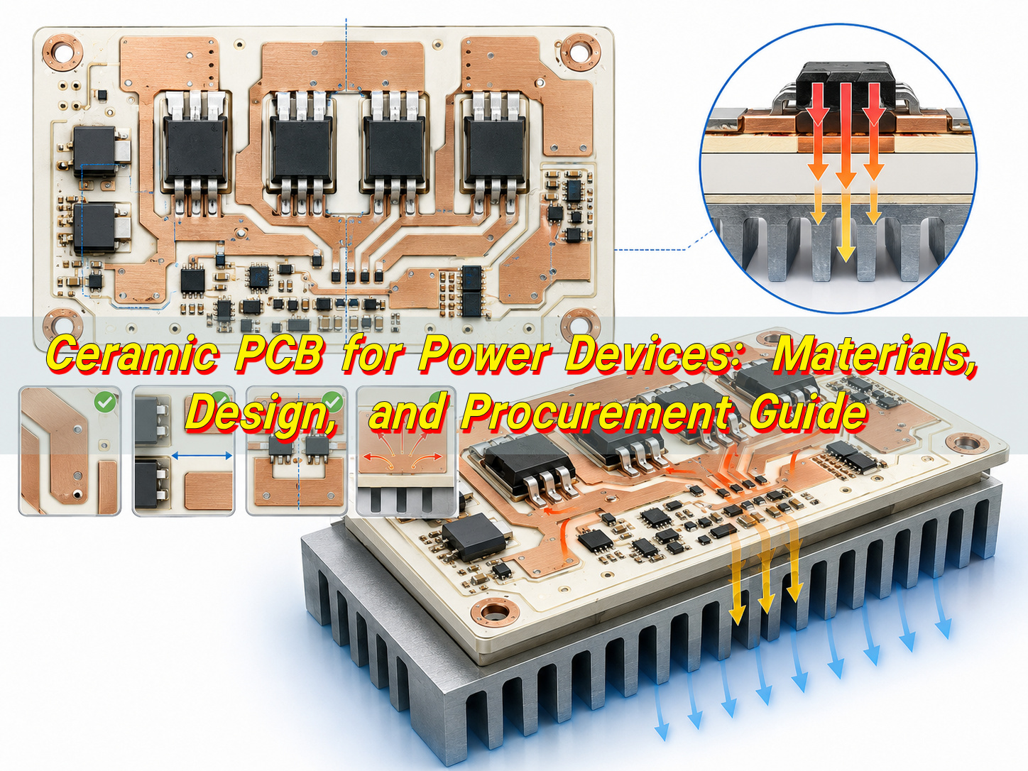
A ceramic PCB for power devices uses a ceramic substrate such as alumina, aluminum nitride, or silicon nitride as the base material. It can dissipate heat faster than common organic laminates, provide stable insulation, and support compact layouts where thermal reliability is a real production concern. The right choice depends on power density, thermal cycling, copper thickness, voltage, device package, assembly method, and cost target.

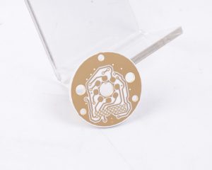
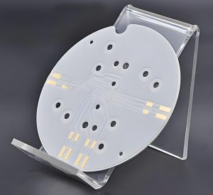
What Is a Ceramic PCB for Power Devices?

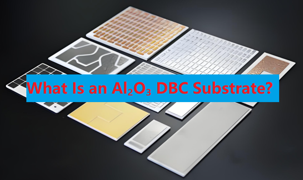
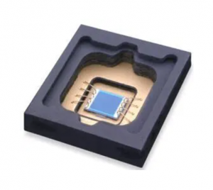
A ceramic PCB for power devices is a circuit board made with a ceramic substrate and metallized conductive layers. Unlike FR4, which uses glass-reinforced epoxy, ceramic boards use inorganic materials that offer high thermal stability, strong dielectric insulation, and excellent dimensional stability.

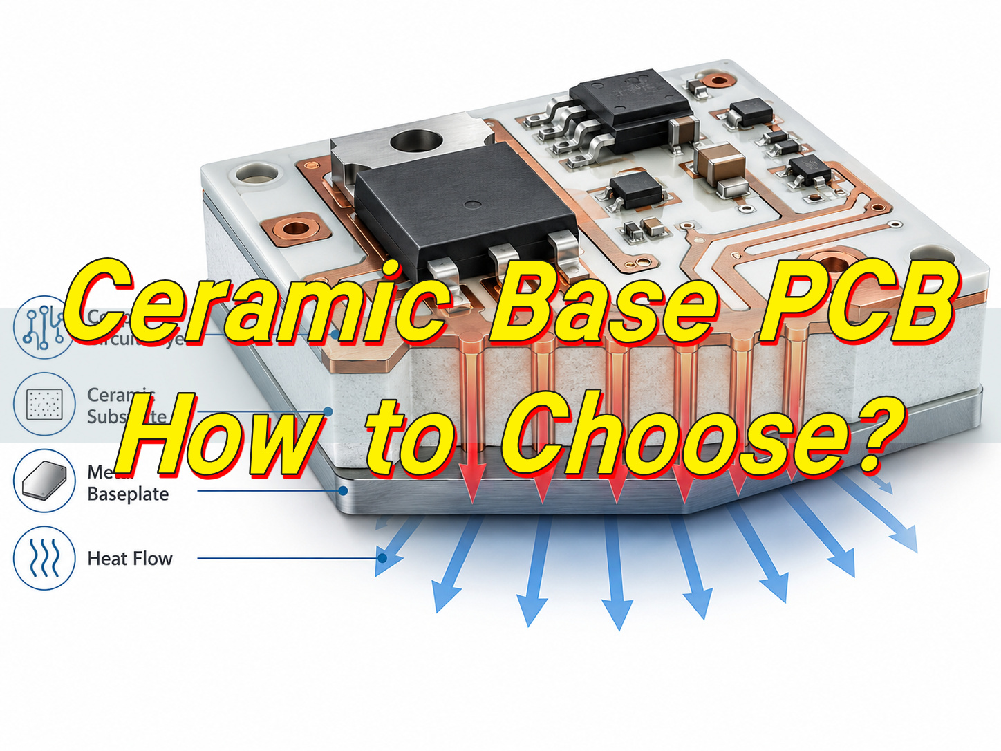
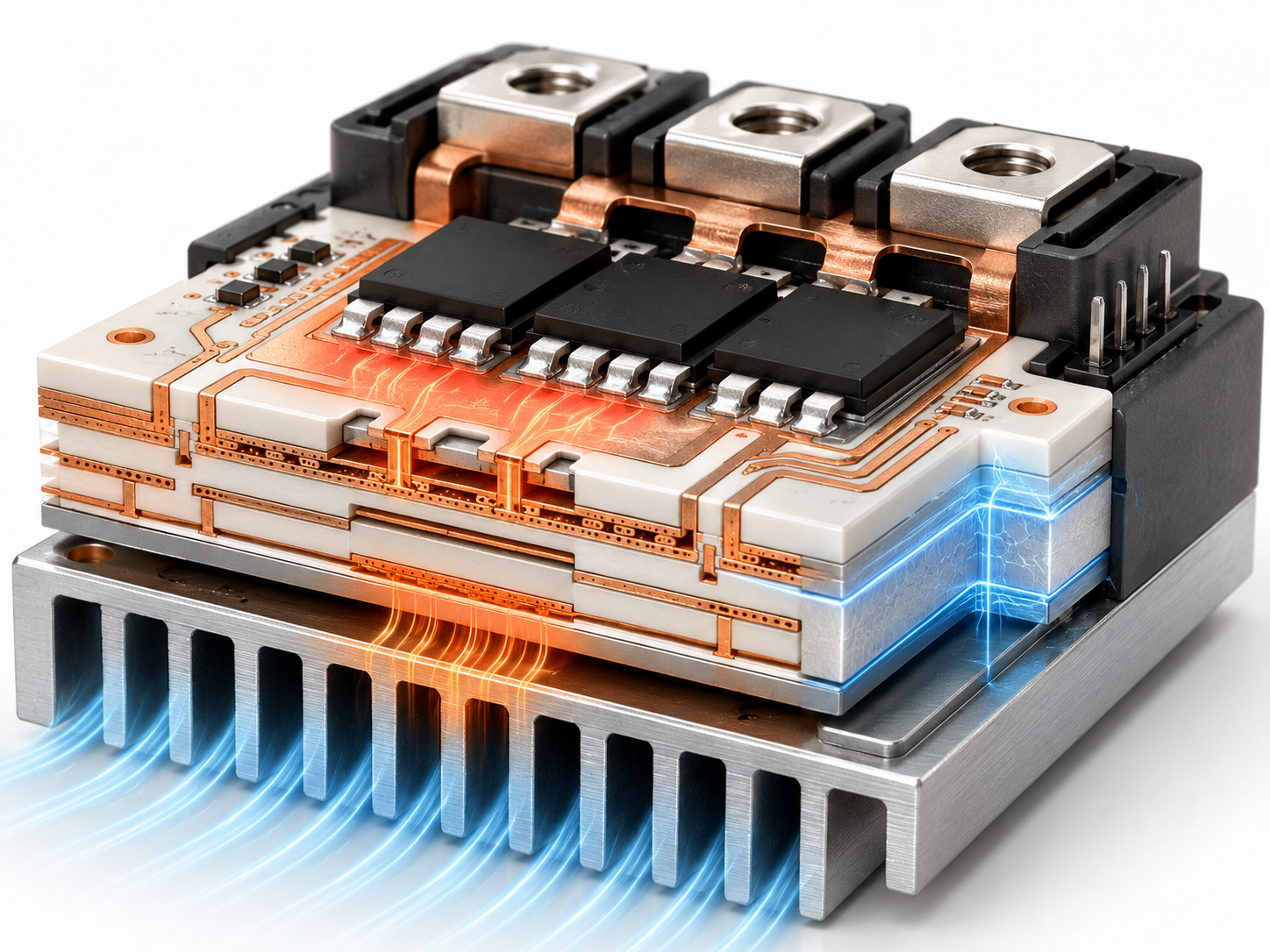
In power electronics, the board is more than a carrier for components. It also becomes part of the heat-transfer path. Heat moves from the semiconductor junction to the package, solder layer, copper circuit, ceramic substrate, thermal interface material, heat sink, and finally the ambient environment.

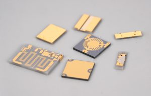
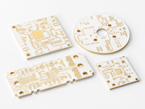
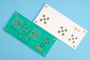
Common ceramic PCB structures for power devices include:

StructureTypical Use
DBC ceramic substrateIGBT modules, power modules, motor drives, inverters
DPC ceramic PCBHigh-precision circuits, LEDs, sensors, compact power modules
AMB ceramic substrateSiC modules, EV power modules, high-reliability power electronics
Thick film ceramic PCBHybrid circuits, resistive circuits, high-temperature electronics
Thin film ceramic PCBFine-line circuits, high-frequency and precision applications

For power devices, the most common discussion usually centers on DBC, DPC, and AMB because they support thermal management, copper bonding, and power module packaging.

Why Do Power Devices Need Ceramic PCBs?

Power devices convert, switch, regulate, or distribute electrical energy. During operation, they generate heat. If heat cannot leave the device efficiently, junction temperature rises, efficiency drops, solder joints age faster, and long-term reliability becomes harder to control.

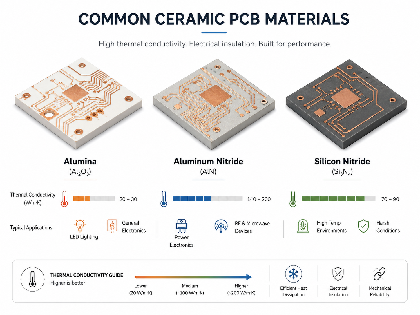
Ceramic PCB helps solve this problem by combining thermal conductivity and electrical insulation in one structure. Aluminum nitride ceramic substrates can offer much higher thermal conductivity than alumina, while silicon nitride provides strong mechanical reliability for demanding thermal cycling environments. Rogers’ ceramic substrate data lists typical thermal conductivity values such as 24 W/mK for Al2O3, 90 W/mK for Si3N4, and 170 W/mK for AlN.

Power devices also need insulation between high-current conductors and the heat sink. Ceramic materials can conduct heat while remaining electrically insulating, which makes them useful for compact power modules where heat and voltage must be managed at the same time.

How Does a Ceramic PCB Work in Power Electronics?

A ceramic PCB works by shortening the thermal path between the power device and the heat sink. In a typical power assembly, copper spreads heat laterally, while the ceramic substrate conducts heat vertically to the cooling structure. The ceramic layer also provides electrical isolation.

Ceramic PCB for Power Devices: Materials, Design, and Procurement Guide

The working logic is simple:

FunctionHow Ceramic PCB Supports It
Heat dissipationCeramic substrate transfers heat away from power chips
Electrical insulationCeramic separates conductive copper from heat sink or housing
Current carryingCopper layer supports power paths and device interconnection
Mechanical supportCeramic base supports chips, solder joints, and terminals
ReliabilityStable material behavior helps resist heat-related deformation

For high-current designs, copper thickness and copper layout matter as much as the ceramic material. A good ceramic substrate with poor copper distribution may still create hot spots. A strong power PCB design should balance thermal spreading, conductor width, copper thickness, clearance, creepage, solder area, and heat sink contact.

What Types of Ceramic PCBs Are Used for Power Devices?

Different ceramic PCB technologies are used for different power levels and manufacturing goals. The best choice depends on the device package, current, voltage, thermal load, circuit accuracy, and reliability requirement.
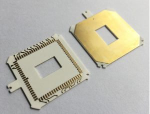
DBC Ceramic PCB

DBC means Direct Bonded Copper. In this process, copper is bonded directly to ceramic through a high-temperature bonding process. It is widely used in power modules because it offers thick copper, good heat spreading, and reliable insulation.

DBC is often used for IGBT modules, rectifier modules, DC-DC converters, motor drives, solar inverters, and industrial power modules.
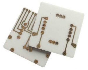
DPC Ceramic PCB

DPC means Direct Plated Copper. It uses thin-film metallization and electroplating to build copper circuits on ceramic. DPC supports finer lines, smaller spacing, plated vias, and higher circuit precision than traditional thick copper ceramic substrates.

DPC is useful for compact power devices, LED modules, sensors, laser modules, and applications where fine circuit features are required.
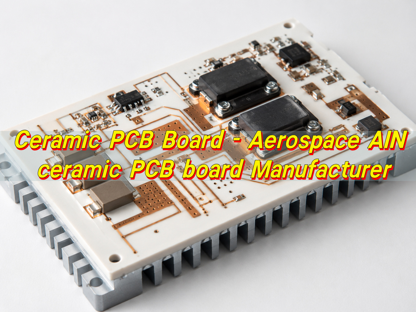
AMB Ceramic PCB

AMB means Active Metal Brazing. It uses active brazing alloy to bond copper to ceramic. AMB is especially valuable for silicon nitride ceramic substrates, where mechanical toughness and thermal cycling performance are important.

AMB ceramic substrates are increasingly used in EV power modules, SiC power modules, traction inverters, renewable energy systems, aerospace electronics, and harsh industrial applications. Ferrotec lists AMB substrates on AlN and Si3N4 and DBC substrates on alumina and AlN for power electronic applications.

Thick Film Ceramic PCB

Thick film ceramic PCB uses screen-printed conductor, resistor, or dielectric pastes fired onto ceramic. It is suitable for hybrid circuits, heating circuits, resistive networks, and some high-temperature electronics.

Thin Film Ceramic PCB

Thin film ceramic PCB uses sputtering, photolithography, and etching to create fine and accurate patterns. It is used when precision, stable impedance, or fine-line geometry is required.

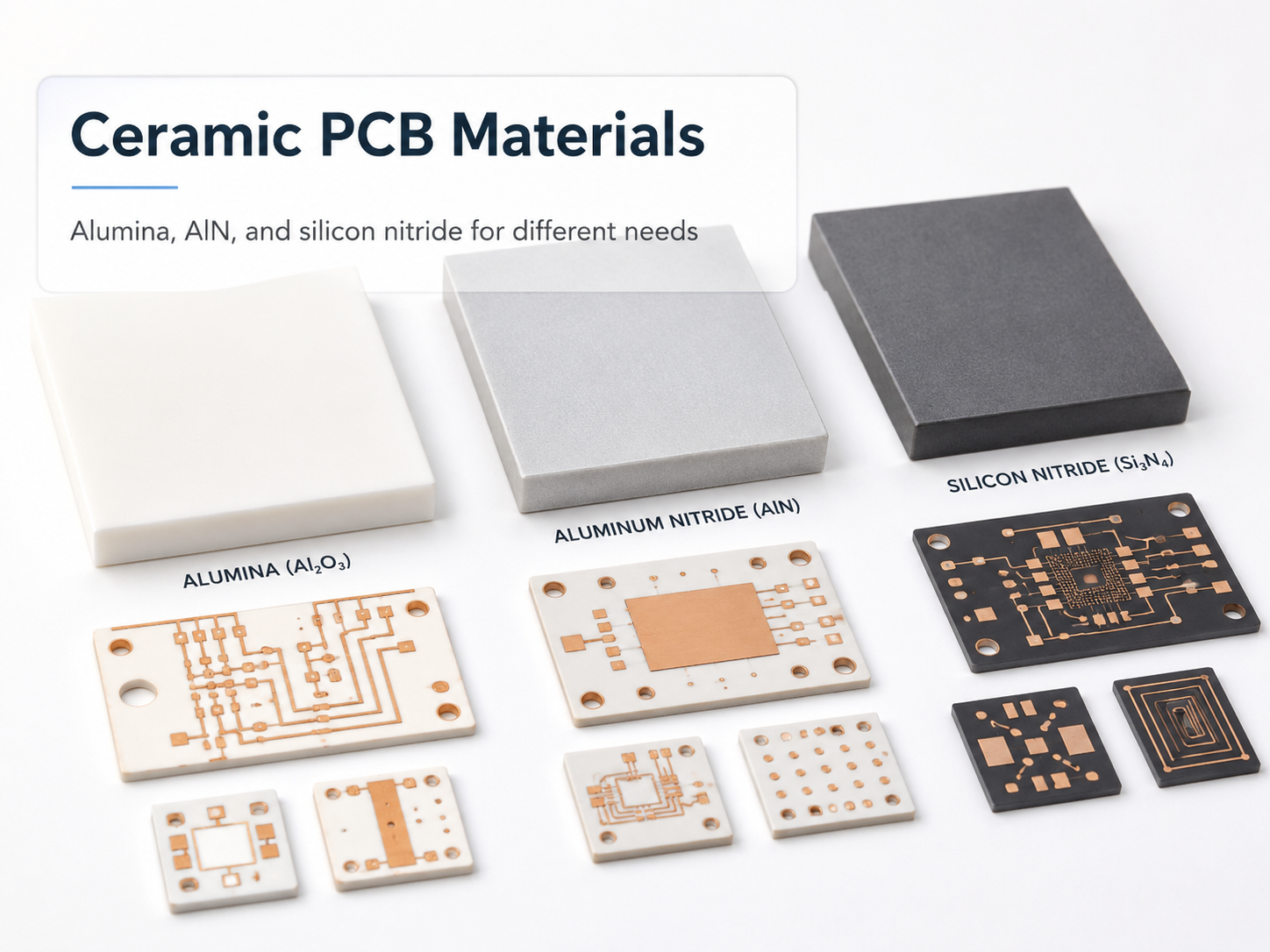
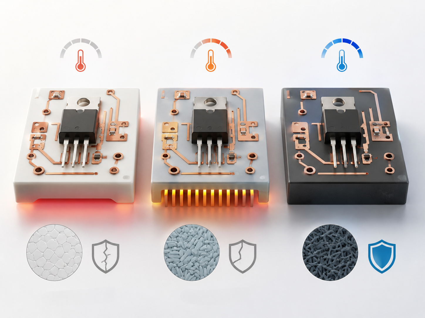
Which Ceramic Materials Are Best for Power Devices?

Material selection is one of the most important decisions in ceramic PCB manufacturing. No single ceramic material is best for every project.

MaterialMain StrengthTypical Power Device UseSelection Note
Alumina Al2O3Cost-effective, stable, widely availableMedium-power modules, LED, industrial electronicsGood balance for cost-sensitive projects
Aluminum Nitride AlNHigh thermal conductivityHigh-power LED, RF power, laser, power modulesBetter for high heat flux
Silicon Nitride Si3N4High toughness and thermal cycling reliabilityEV power modules, SiC modules, harsh environmentsGood for reliability-critical modules
Zirconia-toughened alumina ZTAImproved strength over standard aluminaPower substrates needing better mechanical reliabilityIntermediate option
Beryllium Oxide BeOVery high thermal conductivityLegacy or special applicationsLimited use due to health and handling concerns

Alumina is often selected when the power level is moderate and cost control matters. AlN is preferred when heat dissipation is the main challenge. Si3N4 is selected when thermal cycling, vibration, or mechanical stress is more demanding.

Ceramic PCB for Power Devices: Materials, Design, and Procurement Guide

For SiC and GaN devices, buyers should be especially careful. These devices may operate at higher switching speeds and higher power density. The substrate must support heat transfer, insulation, partial discharge resistance, copper adhesion, and package-level reliability.

What Key Features Should Engineers Check?

A ceramic PCB for power devices should not be selected only by material name. Engineers and buyers should check measurable parameters.

FeatureWhy It Matters
Thermal conductivityAffects heat transfer from device to heat sink
Dielectric strengthSupports voltage isolation
Copper thicknessImpacts current capacity and heat spreading
Copper peel strengthAffects bonding reliability
Ceramic thicknessBalances insulation, thermal resistance, and strength
Surface finishInfluences solderability, wire bonding, and assembly
Warpage controlImportant for chip mounting and module assembly
Line width and spacingDetermines circuit density and manufacturability
Via structureImportant for DPC ceramic PCB and compact modules
Thermal cycling performancePredicts long-term reliability under repeated heating and cooling

For power devices, the most dangerous mistake is focusing only on thermal conductivity. A high thermal conductivity material may still fail if copper thickness, solder joint design, ceramic thickness, or thermal interface control is not suitable.

What Advantages and Limits Should Buyers Understand?

Ceramic PCB has strong advantages, but it is not a universal replacement for every PCB type.

Advantages

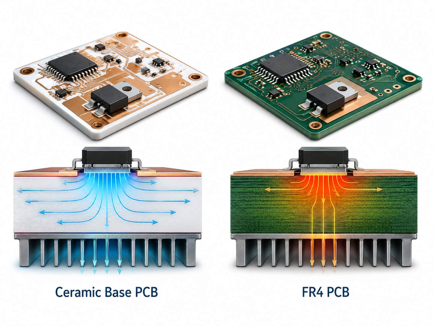
Ceramic PCB offers excellent heat dissipation, strong insulation, good dimensional stability, and better high-temperature performance than many organic board materials. It supports compact power modules where heat needs to move quickly from the device to the heat sink.

It also helps reduce the number of thermal interface layers in some structures. Fewer layers can lower thermal resistance and simplify the thermal path.

Limits

Ceramic materials are harder and more brittle than FR4 or aluminum PCB. Processing, drilling, metallization, and singulation require controlled manufacturing. Cost is usually higher than FR4 or standard metal core PCB. Lead time may also be longer for customized substrates, special copper thickness, tight tolerances, or high-reliability testing.

Ceramic PCB is a strong option when performance justifies the cost. It is not always the lowest-cost solution for low-power products.

How Does Ceramic PCB Compare with FR4, Metal Core PCB, DBC, DPC, and AMB?

Many buyers compare ceramic PCB with FR4 PCB, aluminum PCB, copper substrate PCB, and different ceramic processes. The right answer depends on heat, voltage, current, space, and reliability.

OptionThermal PerformanceElectrical InsulationCost LevelBest Fit
FR4 PCBLow to mediumGoodLowGeneral electronics, control boards
High-Tg FR4 PCBMediumGoodLow to mediumHigher soldering or operating temperature
Aluminum PCBMedium to goodDepends on dielectric layerMediumLED, power supply, moderate thermal load
Copper substrate PCBGoodDepends on dielectric layerMedium to highHigh-power thermal spreading
DPC ceramic PCBGood to excellentExcellentHighFine-line ceramic circuits, compact modules
DBC ceramic PCBExcellent for powerExcellentHighIGBT, inverter, power modules
AMB ceramic PCBExcellent reliabilityExcellentHighSiC, EV, high thermal cycling applications

For many power modules, DBC and AMB are more relevant than ordinary ceramic PCB. For high-precision ceramic circuits, DPC may be more suitable. For simple high-power LED boards, aluminum PCB may still be enough if the thermal requirement is moderate.

How Should You Select the Right Ceramic PCB for a Power Project?

Selection should start with the power device and operating environment. Before choosing Al2O3, AlN, Si3N4, DBC, DPC, or AMB, clarify the real engineering target.

A practical selection path looks like this:

Project RequirementRecommended Direction
Cost-sensitive medium-power boardAlumina ceramic PCB
High heat flux and compact sizeAlN ceramic PCB
High thermal cycling reliabilitySi3N4 AMB ceramic substrate
Thick copper and power module structureDBC ceramic substrate
Fine circuit pattern and plated viasDPC ceramic PCB
Hybrid circuit with printed resistorsThick film ceramic PCB
Fine-line precision circuitThin film ceramic PCB

For procurement teams, the safest method is to share the power device type, voltage, current, heat dissipation target, ceramic material preference, copper thickness, board size, surface finish, assembly method, and annual demand. A factory can then check manufacturability and suggest a stable production route.

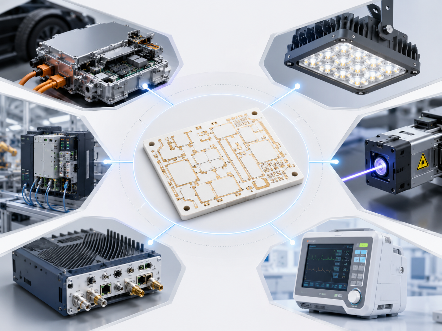
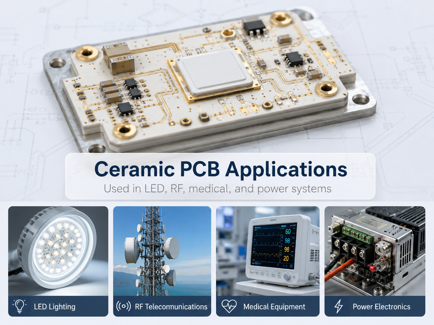
Where Are Ceramic PCBs Used in Power Electronics?

Ceramic PCB is used in industries where heat, current, insulation, and reliability are tied together.

Ceramic PCB for Power Devices: Materials, Design, and Procurement Guide

Electric Vehicles and Charging Systems

EV traction inverters, onboard chargers, DC-DC converters, battery management systems, and charging modules often use high-density power devices. SiC modules and IGBT modules may require ceramic substrates with strong thermal cycling resistance.

Renewable Energy

Solar inverters, wind power converters, and energy storage systems need long service life and stable thermal behavior. DBC and AMB ceramic substrates can support power conversion modules in demanding operating environments.

Industrial Drives and Automation

Motor drives, servo drives, power controllers, welding equipment, and industrial power supplies generate heat during long operation. Ceramic PCB helps improve thermal transfer and insulation.

High-Power LED and Laser Modules

High-power LED, UV LED, laser diode, and optical modules use ceramic PCB to control junction temperature and keep light output stable.

Aerospace and Defense Electronics

These applications may require higher reliability, thermal shock resistance, and stable performance under vibration or temperature cycling.

Medical and Scientific Equipment

Power supply modules, imaging systems, laser modules, and precision instruments may use ceramic PCB when heat control and dimensional stability are important.

What Practical Cases Show Ceramic PCB Value?

A common case is a high-power LED module that suffers from brightness decay and solder fatigue. Replacing a standard board with AlN ceramic PCB can reduce thermal bottlenecks and help maintain more stable heat transfer from the LED chip to the heat sink.

Another case is an EV inverter power module. The module may face repeated heating and cooling during acceleration, braking, charging, and environmental temperature changes. In this situation, Si3N4 AMB may be preferred because mechanical toughness and copper bonding reliability become more important than material price alone.

A third case is a compact industrial power module. The buyer needs thick copper, high insulation, and stable soldering. DBC ceramic substrate can provide a direct thermal path and support high-current operation in a smaller package.

These cases show a clear point: ceramic PCB selection is not only about “higher thermal conductivity.†It is about matching the substrate structure to the failure risk of the actual product.

What Design and DFM Points Matter Before Fabrication?

Ceramic PCB design should be reviewed early because ceramic materials are less forgiving than standard FR4. A small layout decision can affect yield, cost, and long-term reliability.

Important DFM points include:

DFM ItemWhy It Matters
Copper thicknessImpacts etching tolerance, current capacity, and stress
Copper balanceHelps control warpage and thermal stress
Corner radiusReduces stress concentration in copper patterns
Ceramic thicknessBalances insulation, strength, and thermal resistance
Clearance and creepageImportant for high-voltage power devices
Solder pad sizeAffects solder voiding and assembly reliability
Via designCritical for DPC structures
Edge distancePrevents cracking during cutting or handling
Surface finishMust match soldering, wire bonding, or die attach process
PanelizationAffects cost, yield, and production handling

For high-power modules, engineers should avoid sharp copper corners where possible. Rounded copper features can reduce local stress during thermal cycling. For thick copper DBC or AMB substrates, copper pattern geometry should be reviewed with the manufacturer before tooling.

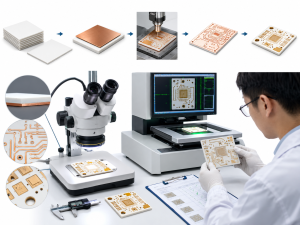
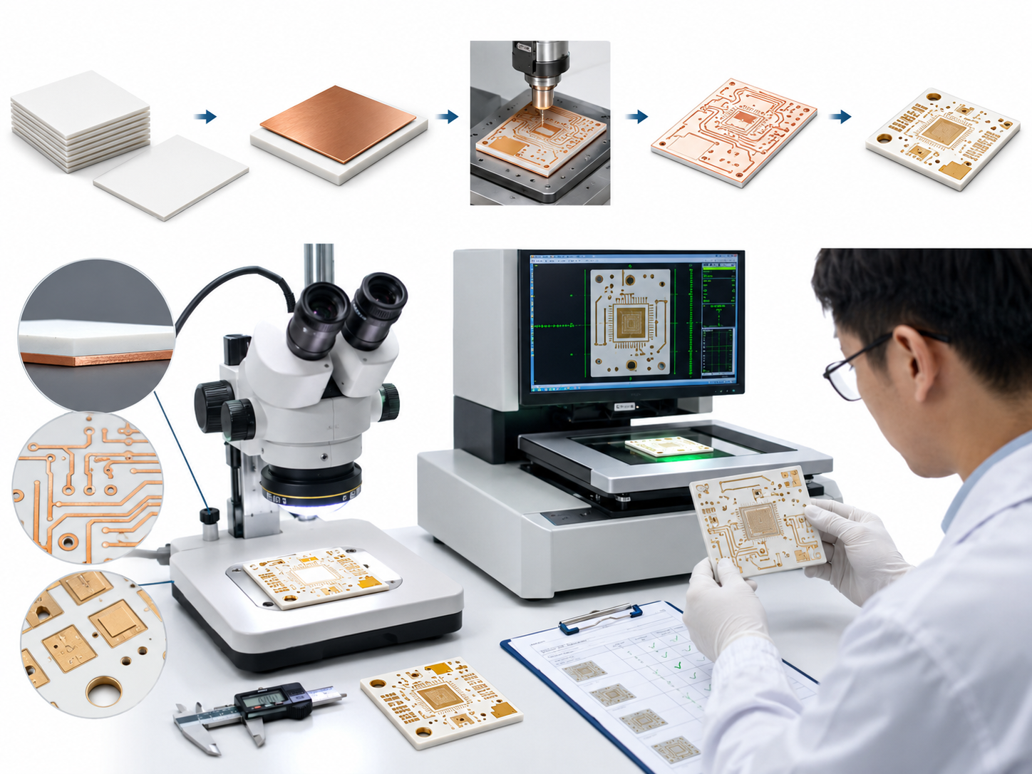
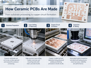
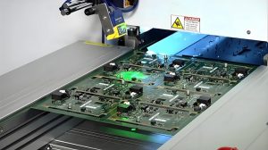
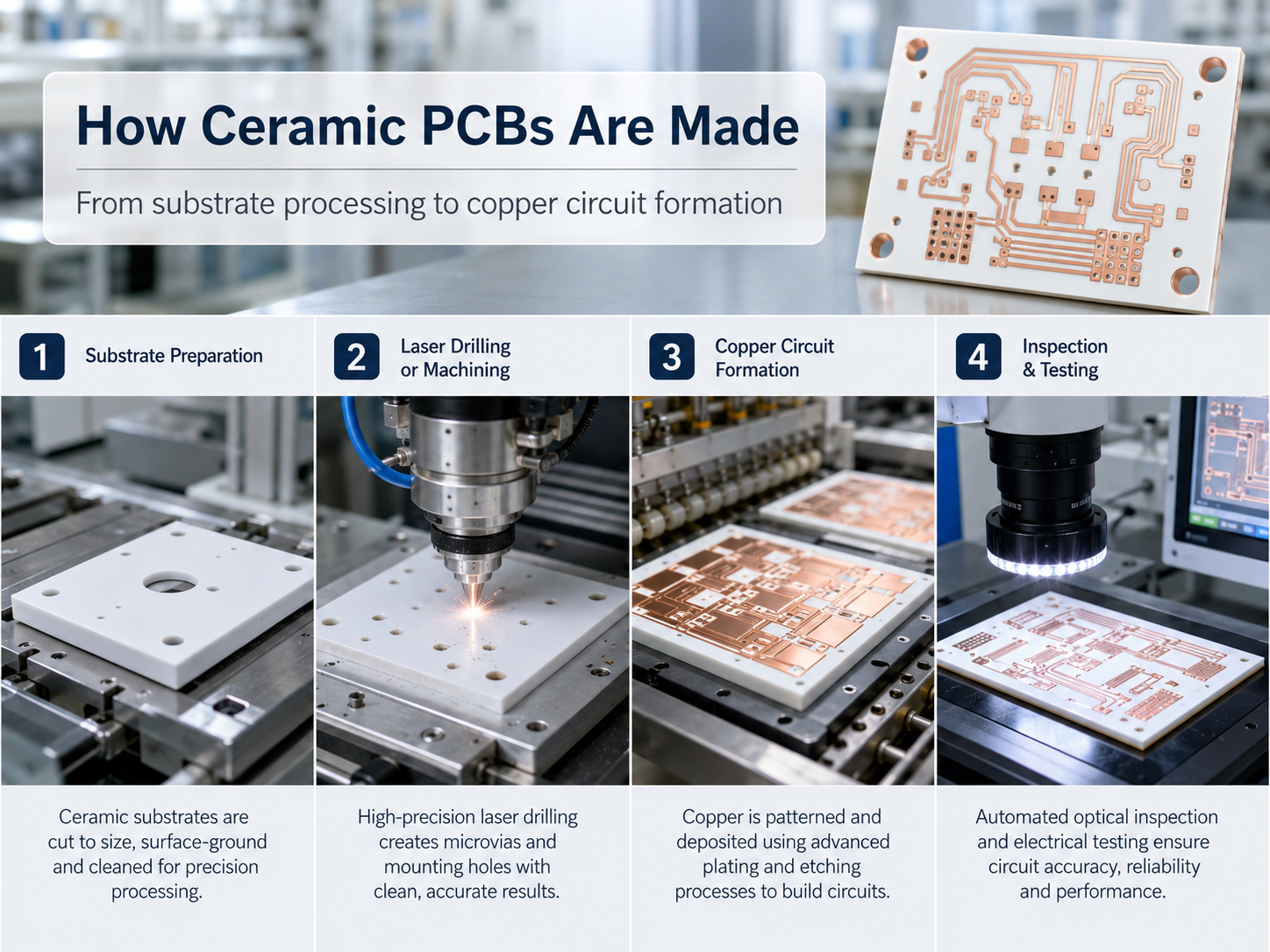
How Are Ceramic PCBs Manufactured and Tested?

Manufacturing depends on the ceramic material and process route. DPC, DBC, AMB, thick film, and thin film all use different production methods.

A simplified manufacturing flow may include ceramic substrate preparation, cleaning, metallization, copper bonding or plating, imaging, etching, drilling or laser processing, surface finishing, inspection, electrical testing, and packaging.

Quality testing should be built around the final use. For power devices, common checks include:

Test or InspectionPurpose
Visual inspectionChecks surface defects, contamination, copper damage
Dimensional inspectionConfirms outline, hole, pad, and pattern tolerance
Electrical testChecks open and short circuits
Insulation resistance testConfirms isolation performance
Dielectric withstand testVerifies high-voltage insulation capability
Copper thickness testConfirms current and thermal design assumptions
Peel strength testChecks copper bonding strength
Solderability testSupports assembly reliability
Warpage measurementHelps control module assembly quality
Thermal cycling testEvaluates reliability under temperature changes
X-ray inspection after assemblyChecks voids, solder joints, and hidden defects

IPC-6012F covers qualification and performance requirements for rigid printed boards, including plating, conductors, holes, acceptance testing, and mechanical and environmental requirements. While ceramic substrates may need project-specific criteria beyond standard FR4 PCB checks, IPC-based inspection language is still useful for documentation and customer communication.

What Failure Modes Should Be Checked in Power Ceramic PCBs?

Power ceramic PCB failure usually comes from heat, stress, poor bonding, contamination, or unsuitable assembly conditions. Failure analysis should look at the whole stack, not only the ceramic board.

Ceramic PCB for Power Devices: Materials, Design, and Procurement Guide

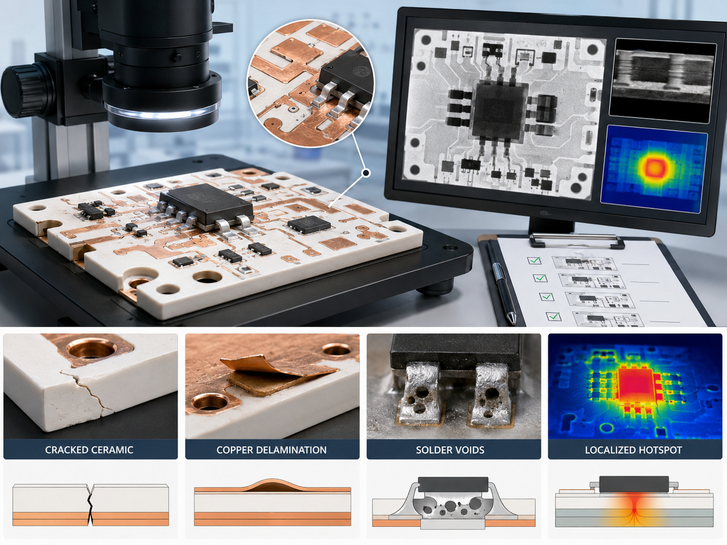
Common failure modes include:

Failure ModePossible CausePrevention Method
Ceramic crackingMechanical shock, poor panel design, edge stressControl handling, edge distance, cutting method
Copper delaminationWeak bonding, thermal cycling, poor process controlVerify peel strength and bonding process
Solder voidingPoor paste control, unsuitable reflow, pad design issueOptimize soldering profile and pad geometry
Hot spotsPoor copper spreading, bad thermal interface, uneven die attachImprove copper layout and thermal path
Insulation breakdownInsufficient ceramic thickness, contamination, voltage stressCheck dielectric strength and cleanliness
Partial dischargeHigh voltage, voids, insulation weaknessImprove insulation design and test criteria
WarpageCopper imbalance, thermal stress, substrate mismatchBalance copper and control process conditions
Surface oxidationPoor storage or finish controlUse proper packaging and surface finish

Thermal cycling is one of the most important reliability concerns. Copper and ceramic expand at different rates. Repeated heating and cooling can create stress at bonded interfaces, solder joints, and copper corners. This is why material toughness, copper geometry, bonding quality, and assembly process control all matter.

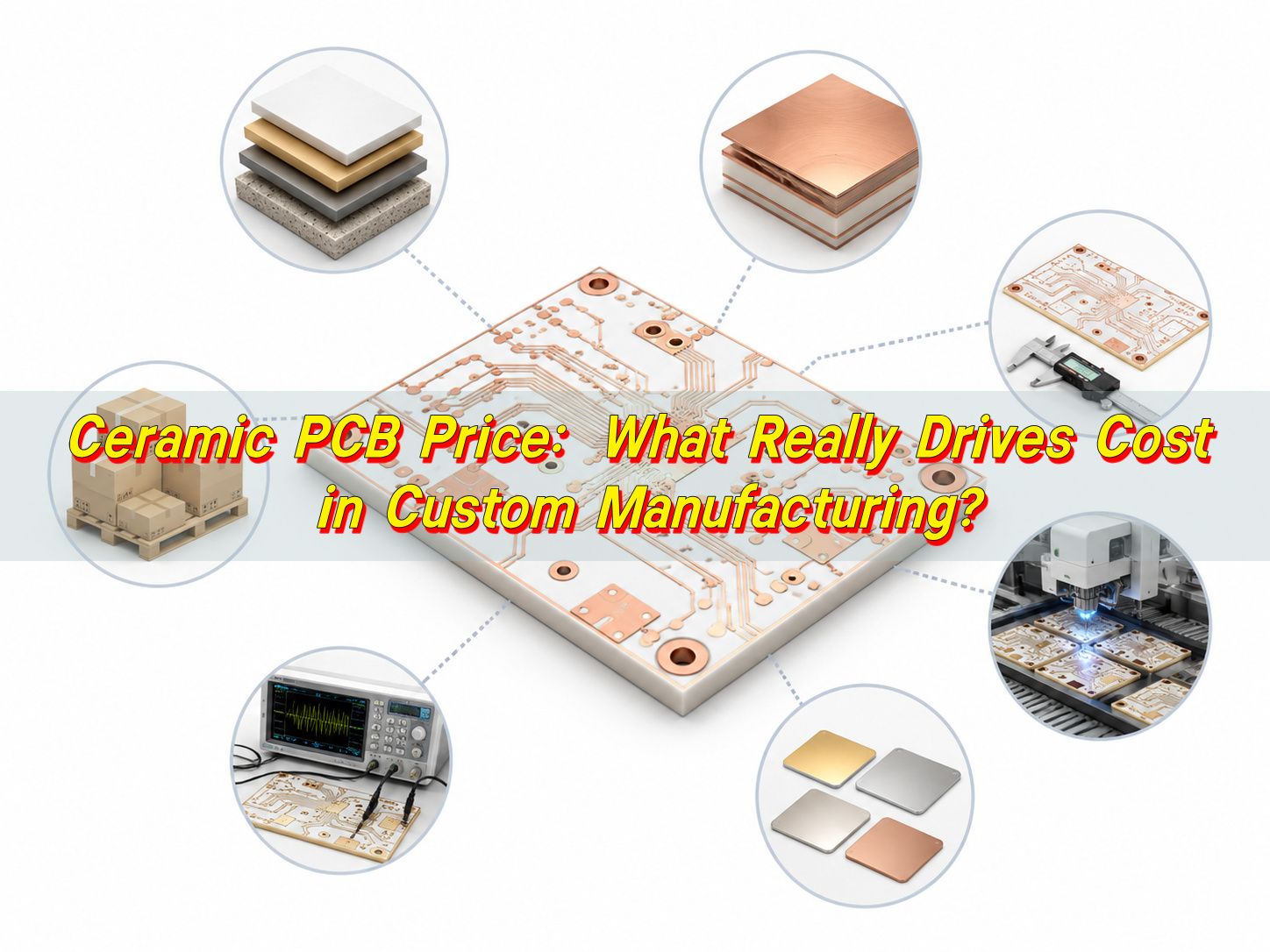
What Affects Ceramic PCB Cost and Lead Time?

Ceramic PCB cost depends on material, process, copper thickness, tolerance, testing, and order volume. AlN and Si3N4 usually cost more than alumina. AMB and DBC substrates also need controlled high-temperature bonding processes, so they are normally more expensive than simple FR4 or aluminum PCB.

Major cost factors include:

Cost FactorImpact
Ceramic materialAl2O3 is usually lower cost; AlN and Si3N4 cost more
Board sizeLarger ceramic panels increase material and yield risk
Copper thicknessThicker copper increases processing difficulty
Circuit toleranceFine lines and tight spacing increase cost
Surface finishENIG, silver, gold, or special finishes affect price
Via structureDPC vias increase process complexity
Testing requirementExtra reliability tests add cost and time
Order quantityPrototype price is higher per piece than batch production
Custom toolingNew shapes and special processes may need tooling
Packaging requirementVacuum packing, dry packing, and export packing add handling steps

A useful cost-control method is to avoid over-specification. For example, do not choose AlN if alumina can meet the thermal target. Do not request ultra-tight tolerance if the module assembly does not require it. Do not use AMB when DBC can meet the reliability requirement.

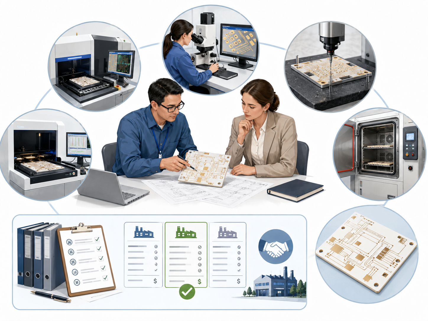
How Can Buyers Choose a Ceramic PCB Supplier?

A good ceramic PCB supplier should understand materials, manufacturing limits, testing, and power electronics reliability. Price matters, but low price without process control can create higher cost later through assembly failure, field returns, or unstable delivery.

Before choosing a supplier, buyers should check:

Supplier CheckWhat to Confirm
Ceramic material capabilityAl2O3, AlN, Si3N4, ZTA availability
Process capabilityDPC, DBC, AMB, thick film, thin film support
Copper capabilityCopper thickness, bonding strength, pattern tolerance
Quality controlElectrical test, insulation test, peel strength, dimensional report
Engineering supportDFM review, stack-up review, material suggestion
DocumentationRoHS, REACH, material data, inspection report
Production experiencePrototype, small batch, and volume manufacturing
Export supportGlobal shipping, packaging, customs documentation
CommunicationFast feedback on technical questions and drawings
Long-term stabilityRepeat production control and traceability

For Europe and North America, buyers often care about compliance documentation, stable repeatability, and long-term quality records. For Southeast Asia and emerging manufacturing regions, lead time, flexible MOQ, and total landed cost can be decisive. A China-based source factory can support global buyers with custom fabrication, batch production, DFM feedback, and export delivery without claiming false local manufacturing locations.

RoHS compliance is also important for many electrical and electronic products. The European Commission states that RoHS currently restricts ten substances in electrical and electronic equipment, including lead, cadmium, mercury, hexavalent chromium, PBB, PBDE, and four phthalates.

What Should Be Checked Before Ordering Ceramic PCB for Power Devices?

Before placing an order, buyers should prepare a clear technical package. This helps the manufacturer quote accurately and reduce engineering back-and-forth.

Recommended order checklist:

ItemRequired Information
ApplicationPower module, LED, inverter, charger, laser, sensor, etc.
Power deviceIGBT, MOSFET, SiC, GaN, diode, LED chip
Ceramic materialAl2O3, AlN, Si3N4, or open for recommendation
ProcessDPC, DBC, AMB, thick film, thin film
Copper thicknessTop and bottom copper thickness
Ceramic thicknessRequired insulation and thermal target
Surface finishENIG, silver, gold, OSP, or other finish
Drawing filesGerber, DXF, mechanical drawing, stack-up
ToleranceLine width, spacing, outline, hole, thickness
TestingElectrical test, Hi-Pot, insulation resistance, thermal cycling
Assembly needsSoldering, wire bonding, die attach, SMT, module assembly
QuantityPrototype, pilot run, mass production forecast
CertificationRoHS, REACH, UL file if applicable, inspection report

A complete file package gives the factory enough information to evaluate manufacturability, cost, and lead time. It also helps prevent wrong material selection and avoids delay before production.

FAQ About Ceramic PCB for Power Devices

Is ceramic PCB better than FR4 for power devices?

Ceramic PCB is better when the project needs high heat dissipation, strong insulation, compact structure, or stable operation under high temperature. FR4 is still suitable for many control circuits and low-to-medium power electronics. The choice depends on power density, temperature rise, voltage, current, cost target, and reliability requirement.

Which ceramic material is best for high-power devices?

Aluminum nitride is often selected for high thermal conductivity. Silicon nitride is preferred when thermal cycling and mechanical toughness are critical. Alumina is a practical choice for medium-power projects with cost control. For EV modules, SiC modules, and harsh environments, Si3N4 AMB is often considered a strong option.

What is the difference between DBC and DPC ceramic PCB?

DBC uses bonded copper and is suitable for thick copper power substrates. DPC uses metallization and plating, allowing finer circuit patterns and plated vias. DBC is common in IGBT and inverter modules. DPC is often used in compact, high-precision ceramic circuits, LED modules, and sensor-related products.

What is the difference between DBC and AMB ceramic substrate?

DBC bonds copper directly to ceramic, usually alumina or AlN. AMB uses active brazing alloy to bond copper to ceramic and is especially useful for Si3N4 substrates. AMB is often chosen for higher reliability under thermal cycling, while DBC is widely used in established power module applications.

Can ceramic PCB carry high current?

Yes, ceramic PCB can support high-current applications when copper thickness, conductor width, thermal path, and bonding quality are properly designed. The ceramic itself provides insulation and heat transfer, while copper carries current. Current capacity should be calculated based on copper geometry, temperature rise, cooling method, and device layout.

Is AlN ceramic PCB always better than alumina ceramic PCB?

No. AlN has much higher thermal conductivity, but alumina is more cost-effective and suitable for many medium-power applications. If the heat load is not extreme, alumina may provide a better cost-performance balance. AlN is more suitable when thermal resistance must be reduced in a compact structure.

Why is silicon nitride used in EV power modules?

Silicon nitride has strong mechanical toughness and good thermal cycling reliability. EV power modules may face repeated temperature changes, vibration, and high power density. Si3N4 AMB substrates can help improve long-term reliability where standard ceramic substrates may be more vulnerable to stress-related cracking.

What surface finish is used on ceramic PCB?

Common surface finishes include ENIG, immersion silver, gold plating, and other application-specific finishes. The right finish depends on soldering, wire bonding, die attach, storage time, and assembly process. For power modules, solderability and bonding compatibility should be confirmed before production.

What causes ceramic PCB cracking?

Cracking may come from mechanical impact, poor edge design, excessive stress during assembly, thermal shock, sharp copper geometry, or unsuitable panelization. Ceramic materials are hard but brittle, so handling, cutting, packaging, and assembly process control are important for yield and reliability.

How can solder voids be reduced on ceramic PCB assemblies?

Solder voids can be reduced through proper pad design, solder paste selection, stencil control, reflow profile optimization, vacuum reflow when needed, and clean surface finish. For power devices, void control is important because voids increase thermal resistance and may create local hot spots.

How much does ceramic PCB cost?

Cost depends on ceramic material, board size, copper thickness, process type, surface finish, tolerance, testing, and quantity. Alumina is usually more economical. AlN and Si3N4 cost more. DBC and AMB structures also cost more than standard FR4 or aluminum PCB because the process is more specialized.

What files are needed for a ceramic PCB quotation?

A complete quotation package should include Gerber files, mechanical drawing, stack-up, material request, copper thickness, ceramic thickness, surface finish, quantity, tolerance, testing requirement, and application notes. If the material is not decided, share the power device, voltage, current, and thermal target for review.

Can ceramic PCB be used for SiC and GaN devices?

Yes. Ceramic PCB is often used for SiC and GaN power devices because these devices can generate high heat density and require strong insulation. Material and process selection should consider switching frequency, voltage stress, thermal cycling, soldering method, and module structure.

How do buyers verify ceramic PCB quality?

Buyers can request dimensional reports, electrical test records, copper thickness measurement, insulation resistance, Hi-Pot testing, peel strength data, solderability checks, and material compliance documents. For power modules, thermal cycling or application-specific reliability testing may also be needed.

How should I choose between a prototype supplier and a mass production factory?

For power ceramic PCB, choose a supplier that can support both engineering validation and repeat production. Prototype speed is useful, but batch consistency matters more for long-term projects. A capable source factory should provide DFM feedback, stable material sourcing, process control, inspection records, and global delivery support.

Conclusion:

Ceramic PCB for power devices is selected when heat dissipation, insulation, current handling, and reliability must work together in a compact structure. Alumina is suitable for cost-sensitive and medium-power applications. Aluminum nitride is better for high heat flux. Silicon nitride, especially with AMB technology, is a strong choice for thermal cycling and harsh operating environments.

For engineering selection, do not judge the board by thermal conductivity alone. Review copper thickness, ceramic thickness, process type, surface finish, insulation distance, soldering method, thermal cycling risk, and test requirements. For procurement, choose a manufacturer that can support DFM review, custom ceramic PCB fabrication, prototype development, batch production, quality documentation, and global delivery from a real China-based source factory.

If you need ceramic PCB for IGBT modules, SiC devices, GaN power devices, high-power LEDs, inverters, chargers, industrial drives, renewable energy equipment, or customized power electronics, working with an experienced ceramic PCB manufacturer can reduce trial-and-error cost and improve production stability.

You may also like

Ceramic PCB Price: What Really Drives Cost in Custom Manufacturing?
Thursday, June 4th, 2026

Ceramic PCB price is not decided by board size alone. It depends on ceramic material, copper structure, metallization method, circuit density, tolerance, quantity, testing scope, and the reliability level required by the final product. For engineers and buyers, the real goal is not to find the lowest unit price. The better goal is to choose a ceramic PCB structure that can handle heat, current, voltage, and long-term operating stress without overpaying for unnecessary specifications.

Ceramic PCB Price: What Really Drives Cost in Custom Manufacturing?

What Is a Ceramic PCB and Why Does Its Price Vary?

A ceramic PCB is a circuit board built on a ceramic substrate instead of conventional FR4 fiberglass material. Common ceramic materials include alumina, aluminum nitride, silicon nitride, LTCC, and HTCC ceramics. These materials are used when a product requires high thermal conductivity, strong insulation, dimensional stability, or better performance in harsh operating environments.

The price varies because “ceramic PCB†is not one single product. A simple single-sided alumina board with printed conductor is very different from an AlN DPC ceramic PCB with laser vias, fine lines, ENIG finish, and tight flatness control. A DBC power module substrate is also different from a thin-film ceramic circuit used in RF or sensor applications.

In other words, ceramic PCB price changes with the engineering requirement. The substrate, copper thickness, pattern precision, via structure, surface finish, testing requirement, yield risk, and order quantity all influence the final quotation.

Why Is Ceramic PCB Price Important for Engineering Decisions?

Ceramic PCB price matters because ceramic substrates are often used in high-value electronics. These products may include power modules, laser systems, medical electronics, RF modules, LED packages, EV components, aerospace electronics, and industrial control equipment.

In these projects, a low board price can become expensive if the material is mismatched. For example, choosing alumina only because it is cheaper may work for moderate thermal loads, but it may not be enough for a high-power module with concentrated heat. On the other hand, selecting AlN or AMB when the design does not need that level of thermal performance may increase cost without improving the final product.

Ceramic PCB Price: What Really Drives Cost in Custom Manufacturing?

A practical quotation should answer three questions: what performance is required, what reliability risk must be controlled, and what structure gives the best cost-performance balance.

How Does a Ceramic PCB Work in Heat and Electrical Control?

A ceramic PCB works by combining electrical insulation with efficient heat transfer. The ceramic base supports the circuit pattern while moving heat away from power components. This is why ceramic boards are widely used in thermal management applications.

In a typical high-power design, heat moves from the component pad into the copper layer, then through the ceramic substrate, and finally into the heat sink or housing. Compared with FR4, ceramic has stronger thermal stability and better dimensional behavior under heat. Compared with many metal-core PCBs, ceramic also provides excellent electrical insulation while supporting compact high-power layouts.

The working principle is simple, but the manufacturing execution is not. Copper bonding, conductor adhesion, ceramic flatness, via metallization, solderability, and thermal cycling behavior all affect reliability. These details are also part of the price.

What Types of Ceramic PCBs Have Different Cost Levels?

Different ceramic PCB technologies have different cost structures. The cheapest option is not always the best, and the most expensive option is not always necessary.

Ceramic PCB TypeTypical UseCost LevelMain Price Driver
Thick film ceramic PCBSensors, resistors, hybrid circuits, general ceramic circuitsLow to mediumScreen printing, paste type, firing cycles
DPC ceramic PCBLED, laser, power control, fine circuit ceramic boardsMedium to highLaser vias, copper plating, line precision
DBC / DCB ceramic PCBPower modules, IGBT, EV power electronicsMedium to highThick copper bonding and substrate size
AMB ceramic PCBHigh-reliability power modules, EV, rail, industrial drivesHighActive metal brazing, bonding strength, thermal cycling demand
LTCC ceramic PCBRF, microwave, compact multilayer modulesHighCo-fired multilayer structure and precision process
HTCC ceramic PCBHigh-temperature packages, aerospace, military-grade electronicsHighHigh-temperature co-firing and metallization system
Thin film ceramic PCBRF, microwave, sensors, high-precision circuitsHighFine-line resolution and deposition control

For price-sensitive projects, thick film or alumina DPC may be enough. For high-power cycling environments, DBC or AMB may offer better long-term value. For RF and compact module designs, LTCC or thin film may justify the higher manufacturing cost.

Which Ceramic Materials Affect Ceramic PCB Price the Most?

Material is one of the strongest price factors. Alumina is usually the most economical ceramic substrate. Aluminum nitride costs more because it offers much higher thermal conductivity. Silicon nitride is often selected when mechanical strength and thermal shock resistance are important.

MaterialCommon NameTypical StrengthCost TendencySuitable Projects
Al₂O₃ 96%AluminaStable insulation, good cost controlLowerLED, sensors, general power electronics
Al₂O₃ 99%High-purity aluminaBetter electrical and surface performanceMediumPrecision circuits, medical, RF support
AlNAluminum nitrideHigh thermal conductivityHigherLaser, high-power LED, power modules
Si₃N₄Silicon nitrideStrong toughness and thermal shock resistanceHigherEV power modules, harsh thermal cycling
LTCC ceramicLow-temperature co-fired ceramicCompact multilayer integrationHigherRF modules, filters, sensors
HTCC ceramicHigh-temperature co-fired ceramicHigh-temperature durabilityHigherPackages, aerospace, extreme environments

Alumina is often selected when the project needs ceramic stability but does not require extreme heat transfer. AlN is selected when thermal resistance must be reduced. Si₃N₄ is often considered when cracking, delamination, or thermal cycling risk is more important than the lowest starting price.

What Manufacturing Processes Change the Final Quote?

The process route can change the price more than the material itself. A small ceramic PCB with simple printed conductors may be relatively economical. The same size board with laser-drilled vias, plated copper, fine-line patterning, and strict inspection can cost much more.

Key manufacturing cost drivers include ceramic cutting, laser drilling, via filling, copper deposition, electroplating, screen printing, firing, photolithography, surface treatment, inspection, and packaging. Fine circuit spacing increases yield pressure. Tight dimensional tolerance requires more process control. Double-sided or multilayer structures add alignment difficulty.

Surface finish also matters. ENIG, gold plating, silver conductor, nickel barrier layers, and special solderable finishes each have different cost implications. For high-reliability applications, the surface finish should be selected based on soldering, wire bonding, storage time, and working environment.

How Do Ceramic PCBs Compare With FR4, MCPCB, DPC, DBC, and AMB?

Ceramic PCB price should not be judged in isolation. It should be compared with the full thermal and reliability requirement of the product.

Ceramic PCB Price: What Really Drives Cost in Custom Manufacturing?
OptionPrice LevelThermal PerformanceInsulationBest Fit
FR4 PCBLowLow to mediumGoodStandard electronics
High-Tg FR4Low to mediumMediumGoodHigher soldering or operating temperature
Aluminum MCPCBMediumMedium to goodDepends on dielectric layerLED lighting and moderate heat dissipation
Copper substrate PCBMedium to highVery goodDepends on insulation systemHigh-power thermal designs
Alumina ceramic PCBMediumGoodExcellentCompact thermal and insulation applications
AlN ceramic PCBHighExcellentExcellentHigh-power and heat-critical designs
DPC ceramic PCBMedium to highGood to excellentExcellentFine circuits, vias, LEDs, laser modules
DBC ceramic PCBMedium to highExcellent for power modulesExcellentThick copper and high current
AMB ceramic PCBHighExcellentExcellentHigh thermal cycling reliability

FR4 wins on cost. MCPCB works well for many lighting and moderate thermal applications. Ceramic PCB becomes valuable when heat, insulation, stability, compactness, or long-term reliability cannot be solved by conventional materials.

How Should Engineers Choose the Right Ceramic PCB Option?

Engineers should start with operating conditions, not only price. The most important details include power density, junction temperature target, insulation voltage, current load, copper thickness, line width, component package, soldering process, and product lifetime.

For a high-power LED module, alumina DPC may be suitable if the heat load is manageable. For a laser diode module, AlN may be preferred because heat concentration is usually higher. For an IGBT or SiC power module, DBC or AMB may be more practical because thick copper and bonding reliability become critical.

The best choice is usually the lowest-cost structure that still meets the thermal, electrical, mechanical, and reliability requirements. Over-specification increases cost. Under-specification increases failure risk.

Where Are Ceramic PCBs Used in Real Industry Projects?

Ceramic PCBs are used in industries where thermal management, insulation, or high-reliability operation is important.

In LED and lighting products, ceramic substrates help transfer heat away from high-brightness chips. In laser modules, they support stable heat spreading and precise assembly. In automotive electronics, ceramic substrates are used in power control, EV charging, battery systems, and high-temperature electronics. In medical electronics, ceramic PCBs may be used in sensors, diagnostic equipment, and compact modules requiring stable electrical behavior.

Ceramic PCB Price: What Really Drives Cost in Custom Manufacturing?

RF and microwave applications may use ceramic circuits because of dielectric stability and low signal loss. Industrial equipment uses ceramic boards in power supplies, motor drives, heating systems, and harsh-environment control modules. Aerospace and defense applications may use ceramic substrates where vibration, heat, and long-term reliability are part of the design requirement.

What Should Be Checked Before Ceramic PCB Fabrication?

Before requesting a ceramic PCB price, buyers should prepare more than Gerber files. A complete quotation package helps the manufacturer evaluate cost accurately and avoid repeated engineering questions.

Useful quotation details include substrate material, ceramic thickness, copper thickness, board size, quantity, surface finish, line width, spacing, hole size, via type, tolerance, solder mask or glass coating requirement, working temperature, insulation voltage, and assembly method. If the board will be wire bonded, the bonding area finish should be clearly specified.

Engineers should also confirm whether the board needs DFM review, impedance evaluation, thermal simulation support, special packaging, 100% electrical test, or reliability testing. These requirements may affect both price and lead time.

How Do Testing and Quality Standards Affect Cost?

Testing increases cost, but it also reduces risk. For ceramic PCBs, common inspections may include visual inspection, dimensional measurement, adhesion test, continuity test, insulation resistance test, solderability check, metallization thickness measurement, thermal shock test, and X-ray inspection for selected structures.

For general PCB quality control, IPC-6012 is widely used for rigid printed board qualification and performance requirements, while IPC-A-600 is commonly used for visual acceptability criteria. IPC-TM-650 provides test methods used across PCB reliability and material evaluation. These standards are not a simple “price add-onâ€; they help define what acceptable quality means before mass production starts.

For ceramic PCBs, the testing plan should match the application. A prototype for lab verification may not need the same testing as an EV power module or medical device assembly. However, skipping essential checks can create hidden cost later.

What Failure Modes Can Increase Hidden Cost?

The visible ceramic PCB price is only one part of project cost. Hidden cost often appears when a board fails during assembly, reliability testing, or field operation.

Common failure modes include ceramic cracking, copper peeling, poor solder wetting, via voids, conductor open circuits, copper-to-ceramic delamination, thermal cycling fatigue, surface contamination, and edge chipping. These failures may come from material mismatch, excessive copper stress, unsuitable surface finish, poor laser drilling quality, aggressive handling, or insufficient process control.

For power applications, copper thickness and ceramic material must be balanced carefully. Thick copper improves current capacity, but it can also increase thermal stress during temperature cycling. For fine circuits, the main risk may be line defects, poor adhesion, or via reliability. A good supplier should review these risks before production, not after failure analysis.

How Can Buyers Control Ceramic PCB Price Without Reducing Reliability?

The most effective way to control ceramic PCB price is to avoid unnecessary specifications while protecting critical performance. Buyers should separate “must-have†requirements from “nice-to-have†requirements.

For example, do not request AlN if alumina can meet the thermal target. Do not specify ultra-tight tolerances if the assembly does not need them. Do not use thick copper if current and thermal performance can be achieved with a thinner copper structure. Do not request complex double-sided vias when a single-sided layout can work.

Ceramic PCB Price: What Really Drives Cost in Custom Manufacturing?

Quantity also affects unit price. Prototype orders carry setup, engineering, tooling, and process preparation cost. Larger batches spread these costs across more boards. If the design is still changing, it is better to start with a controlled prototype, validate performance, then move to optimized batch production.

A practical quotation strategy is to ask for two options: one engineering-safe option and one cost-optimized option. This helps buyers compare price, risk, and production feasibility clearly.

Ceramic PCB Price FAQ

How much does a ceramic PCB cost?

Ceramic PCB cost varies widely because the product can range from a simple alumina substrate to a high-reliability AMB or LTCC multilayer circuit. Board size, material, copper thickness, process type, quantity, surface finish, and testing scope all affect pricing. For custom projects, a reliable supplier usually needs Gerber files, material requirements, quantity, and application details before giving an accurate quote.

Why is ceramic PCB more expensive than FR4 PCB?

Ceramic PCB is more expensive because the raw material is costlier and the manufacturing process is more specialized. Ceramic cutting, laser drilling, metallization, firing, copper bonding, and precision inspection require dedicated equipment and process control. FR4 is suitable for many standard electronics, but ceramic is used when heat, insulation, dimensional stability, or harsh-environment reliability becomes more important than the lowest board price.

Is alumina ceramic PCB the cheapest option?

In most ceramic PCB projects, alumina is the most cost-friendly ceramic substrate. It offers good insulation, stable mechanical properties, and acceptable thermal performance for many LED, sensor, and power control applications. However, alumina is not always the best choice. If the design has high heat concentration or strong thermal cycling stress, AlN, Si₃N₄, DBC, or AMB may provide better long-term reliability.

When should I choose AlN ceramic PCB?

AlN ceramic PCB is suitable when thermal conductivity is a key design requirement. It is often used in laser modules, high-power LEDs, RF power devices, power electronics, and compact thermal designs. Buyers should choose AlN when alumina cannot meet the thermal target. If the heat load is moderate, alumina may still be a more economical choice.

Does copper thickness affect ceramic PCB price?

Yes. Copper thickness affects raw material cost, process difficulty, etching control, plating time, bonding stress, and reliability behavior. Thicker copper can support higher current and better heat spreading, but it may increase stress between copper and ceramic during thermal cycling. The right copper thickness should be selected according to current load, heat path, pad structure, and reliability target.

Is DPC cheaper than DBC?

DPC and DBC have different cost logic. DPC is often used for fine circuits, plated vias, and thinner copper structures. DBC is preferred for power modules that need thick copper and strong current capacity. One is not always cheaper than the other. The final price depends on material, copper thickness, circuit complexity, size, quantity, and testing requirement.

What information is needed for a ceramic PCB quote?

A complete quote should include Gerber files, substrate material, ceramic thickness, copper thickness, board size, quantity, surface finish, tolerance, via requirement, solder mask or coating, working temperature, insulation voltage, and application background. If the product has high reliability requirements, share the thermal cycling, vibration, humidity, or assembly conditions as early as possible.

Can ceramic PCB reduce total product cost?

Yes, in the right application. Ceramic PCB may have a higher board price, but it can reduce heat sink size, improve reliability, simplify thermal design, and lower failure-related cost. For power electronics, LEDs, lasers, and compact modules, the value often comes from system-level performance rather than the bare PCB price alone.

Why do two suppliers give very different ceramic PCB prices?

Different suppliers may quote different materials, process routes, copper thicknesses, finishes, tolerances, testing levels, or lead times. Some quotes may include engineering review and full inspection, while others only cover basic fabrication. Buyers should compare the technical details behind each quote, not only the final number. A low quote with unclear specifications can create production risk.

Is ceramic PCB suitable for high-volume production?

Yes, ceramic PCB can be used for volume production when the design is stable and the process is validated. The key is to control material consistency, metallization quality, dimensional tolerance, yield, packaging, and batch traceability. For high-volume orders, early DFM review and prototype validation help reduce scrap, rework, and late-stage design changes.

How can I reduce ceramic PCB price during design review?

The best methods include simplifying the circuit layout, choosing the right material grade, avoiding unnecessary tight tolerances, optimizing panel utilization, reducing special surface finish requirements, and selecting a process that matches the application. Buyers can also request prototype and batch pricing separately. This helps control early development cost while preparing for scalable production.

What quality checks are important for ceramic PCB orders?

Important checks include dimensional inspection, visual inspection, copper thickness measurement, adhesion verification, electrical continuity, insulation resistance, solderability, and packaging inspection. For demanding applications, thermal cycling, thermal shock, X-ray inspection, and cross-section analysis may be added. The testing plan should match the product risk level instead of using the same checklist for every project.

Conclusion:

Ceramic PCB price should be evaluated as an engineering decision, not only a purchasing number. The right choice depends on material, process, copper structure, reliability target, testing scope, and production volume.

Before placing an order, it is better to share complete Gerber files, material requirements, quantity, and application conditions with an experienced ceramic PCB manufacturer for DFM review and cost optimization.

If you need ceramic PCB prototypes, custom ceramic substrates, small-batch production, or mass manufacturing support, feel free to contact our engineering team. Email: sales@bestpcbs.com

You may also like

Ceramic Base PCB: How to Choose?
Thursday, May 28th, 2026

Ceramic base PCB is used when a circuit board must manage heat, electrical insulation, dimensional stability, or high-frequency performance better than a standard organic substrate. In many power, LED, RF, automotive, medical, and industrial products, the PCB is not only a carrier for components. It also becomes part of the thermal path and reliability design.

Ceramic Base PCB: How to Choose?

EBest Circuit (Best Technology) provides ceramic PCB fabrication, PCB manufacturing, component sourcing, PCBA assembly, DFM support, and testing for projects from prototypes to production.

What Is a Ceramic Base PCB?

Ceramic base PCB is a printed circuit board that uses a ceramic substrate as the main insulating base. Instead of glass-reinforced epoxy, it uses materials such as alumina, aluminum nitride, silicon nitride, or other ceramic substrates. Copper circuits are formed on the ceramic surface through processes such as DPC, DBC, AMB, thick film, or thin film technology.

The ceramic base supports both mechanical and electrical functions. It carries copper traces and components, provides insulation between conductive paths, and helps transfer heat away from active devices. This is why ceramic PCB is often used in high-power and high-reliability products.

A ceramic PCB board may be single-sided, double-sided, or multilayer. Simple LED modules may only require a single-sided structure. Power modules may need thick copper and strong bonding. RF circuits may require stable dielectric properties and controlled impedance.

In sourcing, buyers may use several related terms, such as ceramic PCB board, ceramic base, or even ceramics base. The key is to confirm the actual material, copper thickness, surface finish, tolerance, operating temperature, and assembly requirements before quotation.

Ceramic base PCB is commonly used for high-power LEDs, MOSFETs, IGBTs, laser diodes, RF power amplifiers, sensors, and compact power modules. These devices often generate concentrated heat. A ceramic substrate helps move that heat from the component area to the external cooling structure.

How Is a Ceramic Base PCB Different from a Standard FR4 PCB?

Ceramic base PCB and an FR4 PCB can both carry components and copper circuits, but their substrate materials are different. FR4 uses glass fiber and epoxy resin. Ceramic PCB uses inorganic ceramic material. This difference affects thermal conductivity, temperature resistance, insulation, cost, and manufacturing method.

FR4 is suitable for many standard electronic products because it is economical, mature, and easy to process. It is widely used in consumer electronics, industrial control boards, communication products, and general PCBA projects.

Ceramic Base PCB: How to Choose?

Ceramic PCB is selected when FR4 cannot meet the thermal, electrical, or environmental requirements. It is more common in power electronics, LED modules, RF circuits, semiconductor packaging, automotive electronics, and medical devices.

ItemCeramic Base PCBStandard FR4 PCB
Base materialAlumina, aluminum nitride, silicon nitride, or other ceramic materialGlass fiber reinforced epoxy
Thermal conductivityCommonly about 20–230 W/m·K, depending on materialCommonly about 0.3–0.5 W/m·K
Heat dissipationTransfers heat through the ceramic substrateUsually relies on thermal vias, copper planes, heat sinks, or metal core design
Temperature stabilitySuitable for high-temperature environmentsSuitable for general electronics
Electrical insulationHigh dielectric strengthGood insulation for standard circuits
Dimensional stabilityStable under temperature changeMore affected by thermal expansion and moisture
Processing costHigherLower
Typical usePower modules, LEDs, RF circuits, sensors, automotive, medicalGeneral electronics, control boards, digital circuits, consumer products

The main difference is not only heat dissipation. Ceramic PCB also offers stable electrical behavior, low moisture absorption, and good mechanical stability. These features are useful when the product must work in a compact structure or demanding environment.

Manufacturing is also different. FR4 can be drilled, laminated, plated, routed, and assembled through mature PCB processes. Ceramic is harder and more brittle, so it needs controlled cutting, laser processing, metallization, copper bonding, and careful handling during assembly.

Why Are Ceramic Materials Used as a PCB Base?

Ceramic materials are used as a PCB base because they combine thermal conductivity and electrical insulation. This combination is important for circuits that must move heat away from components without creating electrical leakage or short-circuit risk.

In power electronics, heat usually comes from semiconductor devices, resistors, LEDs, or power ICs. If heat remains near the component, the product may lose efficiency, reduce output stability, or shorten service life. A ceramic base helps create a direct thermal path from the component to the substrate and then to the heat sink or housing.

Ceramic materials also maintain stable performance under high temperature. They have low moisture absorption, good chemical resistance, and reliable dimensional stability. These properties make them useful in industrial, automotive, energy, medical, and aerospace electronics.

For RF and microwave circuits, ceramic PCB materials can also provide stable dielectric properties. This helps engineers control impedance, signal loss, and phase behavior. In antennas, filters, radar modules, and RF power devices, substrate stability directly affects circuit performance.

Main reasons to use ceramic materials as a PCB base include:

  • Better heat transfer than FR4
  • High electrical insulation
  • Stable dielectric properties
  • Low moisture absorption
  • Good dimensional stability
  • Suitability for compact power designs
  • Stable behavior under high temperature

Ceramic is not selected only because it is a premium material. It is selected when the design requires thermal, electrical, or mechanical performance that standard PCB materials cannot provide efficiently.

What Ceramic PCB Materials Are Commonly Used?

Common ceramic PCB materials include alumina, aluminum nitride, silicon nitride, and beryllium oxide. Each material has different thermal conductivity, mechanical behavior, process difficulty, and cost.

Alumina, also called Al₂O₃, is the most widely used ceramic PCB material. It offers good insulation, acceptable thermal conductivity, mature manufacturing support, and a practical ceramic board price. Common grades include 96% alumina and 99.6% alumina. For many LED, sensor, and industrial applications, alumina provides a balanced solution.

Aluminum nitride, also called AlN, is used when heat dissipation is a main requirement. It has much higher thermal conductivity than alumina and has a thermal expansion coefficient closer to silicon. This makes it suitable for high-power LEDs, laser modules, semiconductor packages, and compact power modules.

Silicon nitride, or Si₃N₄, is known for mechanical strength and thermal shock resistance. It is often used in automotive power modules and reliability-focused power electronics. It is useful when the design must handle temperature cycling, vibration, or mechanical stress.

Ceramic Base PCB: How to Choose?

Beryllium oxide, or BeO, has high thermal conductivity, but it requires strict safety control during processing. Because of handling concerns, many projects use aluminum nitride as an alternative when high thermal conductivity is required.

MaterialTypical Thermal ConductivityMain FeaturesCommon Applications
Alumina / Al₂O₃About 20–30 W/m·KMature process, good insulation, controlled costLEDs, sensors, industrial electronics, general ceramic PCB
Aluminum Nitride / AlNAbout 170–230 W/m·KHigh thermal conductivity, good semiconductor compatibilityHigh-power LEDs, laser modules, power modules
Silicon Nitride / Si₃N₄About 60–90 W/m·K depending on gradeHigh mechanical strength, thermal shock resistanceAutomotive power electronics, high-reliability modules
Beryllium Oxide / BeOAbout 200–300 W/m·KHigh thermal conductivity, special handling requirementsSpecialized RF and power applications

Material selection should match the working conditions. Alumina is often suitable for cost-sensitive applications with moderate heat. Aluminum nitride is used when thermal conductivity is critical. Silicon nitride is useful when mechanical reliability is a priority.

A reliable ceramic base PCB manufacturer should not recommend material based only on performance data. It should also consider cost, manufacturability, lead time, copper structure, surface finish, and assembly method.

How Does a Ceramic Base PCB Help with Heat Dissipation?

A ceramic base PCB helps with heat dissipation by forming a shorter and more efficient thermal path between heat-generating components and the external cooling structure. Heat can move from the component pad into the copper layer, through the ceramic substrate, and then into the heat sink, metal housing, or thermal interface material.

In a standard FR4 PCB, heat transfer through the substrate is limited. Engineers often add thermal vias, large copper planes, heat sinks, or metal core structures to improve thermal performance. These methods can work well, but they may require more board space and more design control.

Ceramic substrates have higher thermal conductivity, so they can transfer heat more directly through the board. This is useful in compact power circuits where heat is concentrated in a small area.

Substrate TypeTypical Thermal ConductivityDesign Meaning
FR4About 0.3–0.5 W/m·KSuitable for general circuits; needs additional thermal design for higher power
Aluminum PCB dielectric layerOften about 1–3 W/m·KUseful for LED and power boards, but dielectric layer affects heat transfer
Alumina ceramicAbout 20–30 W/m·KSuitable for moderate to high thermal needs
Aluminum nitride ceramicAbout 170–230 W/m·KSuitable for high-power and compact thermal designs
Silicon nitride ceramicAbout 60–90 W/m·K depending on gradeSuitable when heat transfer and mechanical strength are both important

Copper thickness also affects thermal behavior. Thick copper helps spread heat across the surface. Ceramic helps conduct heat through the substrate. When these two functions are combined properly, the PCB can support higher power density.

Substrate thickness should also be reviewed. A thinner ceramic substrate can reduce thermal resistance, but it must still meet insulation and mechanical strength requirements. A thicker substrate may improve handling strength, but it can increase the thermal path length.

For LED modules, ceramic PCB helps control junction temperature. This supports stable brightness, color performance, and operating life. For power semiconductors, better heat transfer helps reduce thermal stress and improves operating stability.

What Are the Main Benefits of Ceramic Base PCBs?

Ceramic base PCBs provide thermal, electrical, and mechanical advantages for applications that require more than standard PCB performance. Their main value is the ability to conduct heat while maintaining insulation.

The first benefit is thermal conductivity. Ceramic substrates transfer heat more efficiently than FR4. This helps high-power components work within a more controlled temperature range.

The second benefit is electrical insulation. Ceramic materials can provide high dielectric strength while still allowing heat to pass through the substrate. This is useful for power modules, LED arrays, high-voltage circuits, and compact electronics.

The third benefit is dimensional stability. Ceramic substrates expand less than many organic materials under temperature change. This helps maintain circuit accuracy and solder joint stability.

The fourth benefit is environmental stability. Ceramic materials have low moisture absorption and good resistance to many chemicals. This is useful in industrial, automotive, medical, and outdoor applications.

Main benefits include:

  • High thermal conductivity for power-dense designs
  • Good electrical insulation for high-voltage circuits
  • Stable size under temperature change
  • Low moisture absorption
  • Suitable for high-temperature environments
  • Good compatibility with compact modules
  • Stable dielectric behavior for RF designs

Ceramic base PCB is especially useful when thermal management, insulation, and reliability must be handled in the same structure. It can also reduce dependence on large external cooling designs when the product structure allows a direct thermal path.

What Applications Use Ceramic Base PCBs?

Ceramic base PCBs are used in products that require heat dissipation, insulation, compact size, stable signal behavior, or long-term reliability. They are common in LED lighting, power electronics, RF modules, automotive electronics, medical devices, aerospace systems, and sensor modules.

Application AreaCommon UseWhy Ceramic Is Used
LED lightingHigh-power LED, UV LED, automotive lightingHeat dissipation and compact structure
Power electronicsInverters, converters, MOSFET and IGBT modulesThermal transfer and insulation
RF and microwaveAntennas, filters, radar modules, amplifiersStable dielectric properties
AutomotiveEV power units, lighting, sensorsThermal cycling and reliability
Medical electronicsSensors, imaging modules, compact power circuitsStability and process control
Aerospace and UAVRF modules, power control, sensorsWeight, heat, and reliability considerations

EBest Circuit (Best Technology) supports ceramic PCB projects for customers in lighting, industrial control, communication, medical, automotive, and power electronics fields. For these projects, early review of material, copper thickness, thermal path, and assembly method helps improve manufacturability.

How Is a Ceramic Base PCB Manufactured?

Ceramic base PCB manufacturing depends on the substrate material and copper formation process. The main production steps include ceramic substrate preparation, cleaning, metallization, copper formation, circuit patterning, surface finishing, inspection, and profiling.

The process starts with ceramic substrate selection. The factory checks material type, thickness, flatness, surface quality, and dimensional tolerance. A clean and stable surface is important because copper adhesion depends on the substrate condition.

The next step is copper formation or metallization. Different methods are used depending on the design requirement.

DPC, or Direct Plated Copper, uses sputtering and electroplating to form copper on ceramic. It is suitable for fine lines, compact layouts, and precise circuit structures.

DBC, or Direct Bonded Copper, bonds copper foil directly to ceramic at high temperature. It is often used for power electronics because it supports thick copper and higher current capacity.

AMB, or Active Metal Brazing, uses active brazing material to bond copper and ceramic. It is used for high-reliability power modules that require strong bonding.

Thick film technology prints conductive paste on ceramic and fires it at high temperature. It is often used in hybrid circuits and ceramic electronic modules.

Thin film technology forms very fine and accurate circuit patterns. It is suitable for precision applications where tight feature control is required.

Ceramic Base PCB: How to Choose?

A typical process flow includes:

  • Ceramic substrate inspection
  • Surface cleaning and preparation
  • Copper bonding or metallization
  • Circuit imaging and etching
  • Plating and surface finish
  • Laser cutting, drilling, or profiling
  • Electrical testing and visual inspection
  • Dimensional and surface quality check

Design rules vary by process. DPC can support finer features, while DBC is better for thick copper and high-current designs. AMB is selected when bonding strength and reliability are important. The correct process should be chosen based on copper thickness, line width, current load, thermal requirement, and cost target.

What Affects Ceramic PCB Cost?

Ceramic PCB cost is affected by material type, substrate size, ceramic thickness, copper thickness, circuit complexity, surface finish, process type, tolerance, testing, quantity, and assembly requirements. When evaluating ceramic board price, the complete specification is more important than board size alone.

Material is a major factor. Alumina is usually more cost-effective and suitable for many standard ceramic PCB applications. Aluminum nitride costs more because it provides much higher thermal conductivity and requires more controlled processing. Silicon nitride may also cost more due to its mechanical properties and specialized applications.

Copper thickness affects both material usage and process difficulty. Thick copper supports higher current and better heat spreading, but it requires more process control during bonding, etching, and inspection.

Circuit complexity also affects cost. Fine lines, tight spacing, small holes, special shapes, and tight tolerances require more precise production. Surface finish can also change cost, especially when the design requires ENIG, silver, gold, or wire-bondable finishes.

Cost FactorEffect on PricePractical Note
Ceramic materialAlN and Si₃N₄ usually cost more than aluminaSelect material based on actual thermal and mechanical needs
Substrate thicknessNon-standard thickness may increase costUse standard thickness when possible
Copper thicknessThick copper increases material and process costMatch copper to current and heat requirements
Process typeDPC, DBC, AMB, thick film, and thin film have different cost levelsChoose process based on performance and manufacturability
Circuit complexityFine features and tight tolerances increase production difficultyKeep layout practical for the selected process
Surface finishSpecial finishes add costDefine soldering or bonding requirements clearly
QuantitySmall batches have higher unit costUse prototypes for validation, then optimize batch production
Testing and documentationExtra inspection increases cost but improves controlSpecify only required test items

To control ceramic PCB cost, avoid unnecessary over-specification. For example, aluminum nitride may not be required if alumina already meets the thermal target. Very thick copper may not be useful if the current load is moderate. A DFM review can help identify these issues before production.

EBest Circuit (Best Technology) can review ceramic PCB designs before manufacturing. This helps confirm material selection, copper structure, surface finish, panel use, and assembly feasibility. For ceramic PCB projects, early engineering review can improve cost control and production stability.

How Do You Choose a Reliable Ceramic Base PCB Factory?

To choose a reliable ceramic base PCB factory, evaluate its material knowledge, process capability, DFM support, inspection system, traceability, PCBA support, and communication quality. Ceramic PCB production is more specialized than standard FR4 PCB fabrication, so the supplier should understand the design purpose, not only the Gerber files.

First, check material capability. A qualified ceramic base PCB manufacturer should understand alumina, aluminum nitride, silicon nitride, copper thickness options, substrate thickness, thermal conductivity, dielectric properties, and surface finish choices. The supplier should help match the material to heat, voltage, mechanical stress, frequency, and budget.

Second, check process capability. Confirm whether the factory supports DPC, DBC, AMB, thick film, thin film, or the specific ceramic process required by your design. Also check minimum trace and spacing, copper thickness range, hole processing, outline tolerance, and available surface finishes.

Third, check engineering support. Ceramic PCB often needs DFM review before production. The factory should review copper-to-edge spacing, pad design, thermal path, substrate thickness, panelization, soldering method, and assembly handling.

Fourth, check quality control. Useful inspection items include electrical testing, visual inspection, dimensional measurement, copper thickness measurement, adhesion testing, surface finish inspection, and material traceability. For medical, automotive, industrial, or aerospace products, documentation control is also important.

Selection PointWhat to Check
Material knowledgeAlumina, AlN, Si₃N₄, substrate thickness, thermal conductivity
Process capabilityDPC, DBC, AMB, thick film, thin film, copper thickness
DFM supportLayout review, thermal path review, pad design, manufacturability
Quality controlE-test, dimensional inspection, adhesion check, surface finish control
TraceabilityMaterial batch, process records, inspection data
PCBA supportSMT assembly, component sourcing, testing, fixture support
CommunicationClear quotation, technical feedback, delivery updates

EBest Circuit (Best Technology) supports ceramic PCB fabrication, PCB manufacturing, component sourcing, SMT assembly, testing, and one-stop PCBA production. This is useful when the ceramic PCB is part of a complete module and requires coordination between bare board fabrication and assembly.

Before requesting a quotation, prepare Gerber files, drill files, outline drawings, material requirements, substrate thickness, copper thickness, surface finish, quantity, operating temperature, voltage, current load, thermal target, and assembly notes. If the material has not been finalized, provide the application background so the factory can recommend a practical option.

To summarize, ceramic base PCB is suitable for designs that require better heat dissipation, electrical insulation, dimensional stability, and reliability than standard FR4 can provide. Alumina is often used for balanced cost and performance, aluminum nitride is used for high thermal conductivity, and silicon nitride is suitable for mechanically demanding applications. For ceramic base PCB fabrication, ceramic PCB board manufacturing, or PCBA project support, contact EBest Circuit (Best Technology) at sales@bestpcbs.com for quotation and engineering review.

You may also like

Ceramic PCB Board – Aerospace AlN Ceramic PCB Board Manufacturer
Monday, May 18th, 2026

Ceramic PCB board is a high-performance circuit board built on a ceramic substrate instead of a conventional glass-fiber epoxy base. It is often selected when an electronic product needs excellent heat dissipation, dimensional stability, high insulation strength, and long-term reliability under demanding operating conditions. For aerospace electronics, power modules, RF devices, LED systems, medical equipment, and high-temperature industrial applications, ceramic circuit boards offer a strong foundation for designs where thermal and electrical performance matter from the first prototype to full production.

Ceramic PCB Board - Aerospace AlN Ceramic PCB Board Manufacturer

EBest Circuit (Best Technology) supports ceramic PCB fabrication, ceramic PCB prototype builds, ceramic substrate circuit board PCB PCBA projects, and engineering-driven manufacturing support for customers who need stable, production-ready solutions.

What Is a Ceramic PCB Board?

Ceramic PCB board is a printed circuit board that uses ceramic as the base substrate. The ceramic layer replaces the traditional FR4 laminate and provides stronger thermal conductivity, higher temperature resistance, and better electrical insulation. Conductive traces are formed on the ceramic surface through copper bonding, thick-film printing, thin-film metallization, or direct plated copper processes, depending on the application and performance target.

The main role of a ceramic PCB is to carry electronic circuits while also helping the product handle heat, stress, and electrical load more effectively. This makes it valuable for applications where a normal FR4 PCB may not provide enough thermal transfer or dimensional stability.

Ceramic circuit boards are often used in devices that must remain reliable for many years. These include aerospace power modules, RF amplifiers, laser systems, LED lighting modules, semiconductor test equipment, medical sensors, and industrial control products.

A ceramic PCB board may be supplied as a bare ceramic circuit board or as a fully assembled PCBA. A bare PCB board ceramic substrate includes the ceramic base, copper circuits, vias or pads if required, surface finish, and final inspection. A completed ceramic PCBA adds components, soldering, inspection, testing, and packaging. This full-process capability is useful when a customer wants one supplier to control fabrication, component sourcing, assembly, and quality verification.

How Is a Ceramic PCB Board Different from a Standard FR4 PCB?

Ceramic PCB board and an FR4 PCB both provide electrical interconnection, but they are designed for different performance levels. FR4 is a glass-reinforced epoxy laminate widely used in consumer electronics, control boards, communication devices, and general industrial products. It is affordable, easy to process, and suitable for many standard designs.

The biggest difference is the substrate. FR4 has relatively low thermal conductivity. It can work very well in many electronic products, but it does not move heat as quickly as ceramic. Ceramic materials such as aluminum nitride and alumina provide much stronger thermal paths.

Comparison ItemCeramic PCB BoardStandard FR4 PCB
Base MaterialAlumina, aluminum nitride, silicon nitride, or other ceramic substrateGlass fiber reinforced epoxy laminate
Thermal ConductivityHigh to very high, depending on ceramic materialLow, usually suitable for moderate heat loads
Temperature ResistanceExcellent for high-temperature environmentsGood for standard electronics, limited at higher temperatures
Electrical InsulationStrong insulation with good dielectric strengthGood insulation for common circuit designs
Dimensional StabilityVery stable under heatMore expansion under thermal stress
Typical ApplicationsAerospace, power electronics, RF, LED, medical, laser, semiconductor modulesConsumer electronics, general industrial boards, communication products
Cost LevelHigher because of material and process complexityLower and widely available
Prototype ConsiderationRequires careful design review and manufacturer experienceFaster and easier for common PCB factories
Assembly NeedsRequires controlled soldering and thermal process knowledgeMature and common SMT process flow

The choice is not about which material is always better. It is about whether the design needs the extra performance. For a simple control board with low heat, FR4 is often a smart choice. For a compact power module or aerospace AlN ceramic PCB board, ceramic can offer a stronger long-term solution.

What Are Ceramic Circuit Boards Used For?

Ceramic circuit boards are used in products where heat, power density, precision, and reliability must be controlled carefully. They are often found in industries that value stable performance over the full product life cycle.

In aerospace electronics, ceramic boards are used in power control modules, RF communication devices, sensor systems, radar-related circuits, and high-reliability control units. These products often work in environments with temperature changes, vibration, and strict weight limitations. A ceramic PCB can help engineers reduce thermal stress and improve circuit stability.

In power electronics, ceramic circuit boards are used for MOSFETs, IGBTs, power converters, motor drives, solid-state relays, and high-current modules. The ceramic substrate helps transfer heat from the power device to the heat spreader or housing. This supports smaller designs and more stable operating temperatures.

Ceramic PCB Board - Aerospace AlN Ceramic PCB Board Manufacturer

Common applications include:

  • Aerospace power modules, RF units, avionics sensors, and satellite-related electronic assemblies.
  • High-power LED modules, UV LED curing systems, automotive lighting, and industrial lighting engines.
  • RF and microwave circuits, including amplifiers, filters, antennas, and high-frequency ceramic substrate modules.
  • Medical electronics such as imaging equipment, sensor modules, laser systems, and diagnostic devices.
  • Semiconductor equipment, probe cards, laser diode carriers, and precision measurement instruments.
  • New energy products, charging modules, power conversion units, and thermal management assemblies.

Ceramic PCB boards are also widely used in high-end lighting. For example, LED chips generate concentrated heat. If that heat stays near the junction, brightness and life span can be affected. In RF applications, ceramic materials offer stable dielectric behavior. This is useful for circuits where signal loss, impedance control, and frequency stability are important.

What Ceramic PCB Materials Are Commonly Used?

The most common ceramic PCB materials include alumina, aluminum nitride, silicon nitride, and sometimes beryllium oxide in special legacy or niche applications. For modern commercial and industrial projects, alumina and aluminum nitride are the most widely used because they offer a practical balance of performance, manufacturability, availability, and cost.

Alumina ceramic, often written as Al₂O₃, is the most familiar option. It offers good insulation, good mechanical strength, stable performance, and a cost level that is more accessible than aluminum nitride. Common purities include 96% alumina and 99% alumina.

Aluminum nitride, written as AlN, is used when much higher thermal conductivity is required. Some buyers may search for an “aluminum nitride AIN ceramic PCB board,†although the correct chemical abbreviation is AlN. This material is especially attractive for aerospace, high-power LED, RF, laser, and power semiconductor applications. It offers excellent heat transfer while maintaining electrical insulation.

Ceramic PCB Board - Aerospace AlN Ceramic PCB Board Manufacturer

Silicon nitride is known for strong mechanical toughness and thermal shock resistance. It can be useful in applications where the board may face mechanical stress, impact risk, or repeated heating and cooling.

A simple way to view the material choices is this:

Ceramic PCB MaterialMain StrengthTypical Use CaseCost Tendency
96% AluminaGood insulation, stable processing, balanced costLED modules, sensors, industrial electronics, general ceramic PCB prototypeModerate
99% AluminaBetter purity, stronger electrical performancePrecision circuits, medical modules, high-reliability electronicsModerate to higher
Aluminum NitrideExcellent thermal conductivityAerospace, power modules, RF, laser diodes, high-power LEDHigher
Silicon NitrideHigh toughness and thermal shock resistanceHarsh mechanical or thermal environmentsHigher
Beryllium OxideVery high thermal performance but special handling concernsLimited specialized applicationsSpecial-case material

When selecting ceramic PCB materials, engineers should not only compare thermal conductivity values. They should also review copper bonding method, via structure, surface finish, operating voltage, component type, board size, tolerance, and assembly process.

What Is an Aluminum Nitride AlN Ceramic PCB Board?

An aluminum nitride AlN ceramic PCB board is a circuit board made with an AlN ceramic substrate. It is selected mainly for its excellent thermal conductivity and strong electrical insulation. For products that generate concentrated heat, AlN can help transfer heat away from components while still keeping the circuit electrically isolated.

AlN ceramic PCB boards are often used in aerospace electronics, laser diode modules, RF power amplifiers, high-brightness LED systems, power semiconductor packages, and new energy modules. In these products, heat is not just a side issue. It is one of the main factors that shapes the product’s service life, efficiency, and safety margin.

Aerospace applications are a strong fit for AlN because engineers often need compact and lightweight solutions. They also need materials that can perform through temperature changes and long operating cycles. An aerospace AlN ceramic PCB board can support this goal by combining thermal efficiency with a stable ceramic platform.

However, AlN projects require careful manufacturing control. The material is harder and more brittle than organic laminates, so drilling, cutting, metallization, and handling must be done with suitable process knowledge. Copper adhesion, surface flatness, laser processing, and final inspection are also important.

EBest Circuit supports aluminum nitride ceramic PCB manufacturing for customers who need high thermal performance, stable process control, and engineering communication during the design-to-production stage. For aerospace or other high-reliability projects, early DFM review is especially useful because it can help refine copper layout, board thickness, surface finish, and assembly method before production begins.

When Should You Choose Alumina Ceramic PCB Materials?

Alumina ceramic PCB materials are a strong choice when the design needs better thermal performance than FR4, good electrical insulation, stable mechanical properties, and a more economical ceramic option than AlN. Alumina is widely used because it offers a practical balance between performance and cost.

You may choose alumina when the heat load is moderate to high but does not require the premium thermal performance of aluminum nitride. It is common in LED modules, sensor boards, power control circuits, thick-film ceramic circuits, medical devices, and industrial electronics.

Alumina is available in different purity levels. A 96% alumina ceramic substrate is popular because it is cost-effective and reliable for many applications. A 99% alumina substrate can offer better purity and performance for more demanding circuits.

Before choosing alumina, engineers should review several points:

  • Thermal requirement: Alumina is better than FR4, but AlN is stronger for very high heat transfer.
  • Circuit density: Fine traces may require a more precise metallization process.
  • Operating environment: Alumina performs well in high-temperature and stable insulation applications.
  • Cost target: Alumina often supports a more controlled ceramic board price than premium ceramic materials.
  • Assembly plan: Component size, soldering profile, and thermal mass should be reviewed early.

Alumina is also suitable for ceramic PCB prototype projects. When a customer wants to validate a ceramic design before mass production, alumina can provide a dependable starting point. It allows engineers to test thermal behavior, mechanical fit, surface finish, solderability, and electrical function without immediately moving to a more expensive material.

What Is a Bare PCB Board Ceramic Substrate?

A bare PCB board ceramic substrate is a ceramic circuit board before electronic components are assembled. It includes the ceramic base, conductive circuits, pads, vias if required, and surface finish.

For a ceramic PCB, the bare board stage is especially important. The substrate material, copper bonding, circuit pattern accuracy, hole quality, surface finish, and inspection process all affect the final PCBA. If the bare ceramic circuit board is not controlled properly, assembly yield and long-term reliability can be affected.

A bare ceramic board may use several circuit-forming technologies. Thick-film ceramic circuits are made by printing conductive paste and firing it at high temperature. Thin-film ceramic circuits use vacuum deposition and etching to create fine patterns. DBC, or direct bonded copper, bonds copper directly to ceramic at high temperature and is often used for power modules. DPC, or direct plated copper, can create more precise copper features and plated vias for advanced designs.

The surface finish is also important. Common options may include ENIG, silver, gold plating, nickel plating, or other finishes depending on soldering and bonding needs. For wire bonding, the finish must support reliable bond strength.

A bare PCB board ceramic product is often ordered by customers who handle assembly internally or send it to another EMS provider. However, many customers now prefer one-stop support because ceramic boards require closer coordination between fabrication and assembly.

EBest Circuit provides bare ceramic PCB board manufacturing as well as assembled ceramic PCBA service. This helps customers move from ceramic substrate design to finished electronic module with better process continuity.

How Is a PCB Ceramic Circuit Board Manufactured?

A PCB ceramic circuit board is manufactured through a controlled process that depends on the ceramic material, copper structure, circuit density, and end application.

The manufacturing journey usually begins with engineering review. The manufacturer checks the Gerber files, stackup, substrate material, copper thickness, hole design, surface finish, tolerances, and assembly requirements. After the review, the ceramic substrate is prepared. The substrate must meet thickness, flatness, and surface quality requirements. Depending on the process, the circuit layer may be created by printing conductive paste, bonding copper foil, sputtering metal layers, or plating copper.

Typical manufacturing steps include:

  • Material selection and DFM review based on thermal, electrical, and mechanical requirements.
  • Ceramic substrate preparation, cleaning, thickness control, and surface inspection.
  • Circuit formation through thick film, thin film, DBC, DPC, or another suitable process.
  • Hole processing, laser drilling, mechanical drilling, or via formation where required.
  • Copper patterning, etching, plating, or metallization control according to the design.
  • Surface finish application for soldering, wire bonding, or corrosion protection.
  • Electrical test, dimensional inspection, visual inspection, and packaging.

For DBC ceramic boards, copper is bonded to ceramic at high temperature. This method is excellent for power electronics because it supports thicker copper and strong thermal paths. For DPC ceramic boards, copper is built through plating, which can support finer features and plated vias. For thin-film ceramic boards, the process can create very precise patterns for RF, sensor, and high-frequency applications.

Ceramic PCB Board - Aerospace AlN Ceramic PCB Board Manufacturer

Can Ceramic PCB Boards Support PCBA Assembly?

Yes, ceramic PCB boards can support PCBA assembly, and many ceramic projects are built as complete assembled modules. In fact, ceramic substrates are often selected because they provide a better base for high-power components, LEDs, RF devices, sensors, and semiconductor packages.

Ceramic PCBA assembly requires more process attention than standard FR4 assembly. The board has different thermal behavior, higher rigidity, and lower flexibility. Soldering profiles must be controlled carefully because ceramic substrates conduct and absorb heat differently. Components with large thermal pads, power packages, or bottom terminations may need special stencil design and solder paste control.

SMT assembly on ceramic boards can include LEDs, ICs, resistors, capacitors, MOSFETs, sensors, connectors, and custom components. Some designs may also use wire bonding, die attachment, or hybrid assembly methods.

For ceramic substrate circuit board PCB PCBA projects, the best results usually come from close cooperation between the board manufacturer and assembly team. Pad design, surface finish, solder paste type, reflow curve, component thermal path, and inspection method should be considered together. A ceramic PCB can also support testing after assembly. Depending on the product, testing may include visual inspection, AOI, X-ray inspection, electrical testing, functional testing, thermal testing, or reliability screening..

EBest Circuit (Best Technology) offers one-stop PCB and PCBA manufacturing support, including ceramic PCB fabrication, component sourcing, SMT assembly, testing, and engineering communication. For customers who need both bare board ceramic substrates and assembled modules, this integrated support can reduce coordination gaps and help the project move faster from prototype to production.

How Do You Choose a Reliable Ceramics PCB Board Manufacturer?

Choosing a reliable ceramics PCB board manufacturer requires more than comparing unit price. Ceramic boards involve special materials, precision processing, thermal design, and assembly knowledge. A low quote may look attractive at the beginning, but the real value comes from stable quality, clear communication, process capability, and the ability to support your product through prototype and production.

First, review the manufacturer’s ceramic material experience. A capable supplier should understand alumina, aluminum nitride, and other ceramic PCB materials. They should be able to explain which material fits your application and why.

Second, check the process capability. Different ceramic circuit boards may require DBC, DPC, thick-film, thin-film, laser drilling, copper plating, precision cutting, or special surface finishes.

Third, evaluate engineering support. Ceramic PCB designs often benefit from DFM review before production. A good engineering team can help check pad design, thermal path, board thickness, surface finish, panelization, and manufacturability.

Fourth, confirm quality control and traceability. For aerospace, medical, industrial, and power electronics, documentation matters. Inspection records, material control, electrical testing, dimensional reports, and production traceability can give customers more confidence.

EBest Circuit (Best Technology) is positioned as an engineering-driven PCB and PCBA manufacturing partner. The company supports ceramic PCB board fabrication, ceramic circuit boards, ceramic PCB prototype builds, PCB ceramic circuit board production, component sourcing, PCBA assembly, and testing. For customers working on aerospace AlN ceramic PCB boards, LED thermal modules, power electronics, medical devices, or industrial control products, EBest provides practical support from design review to production delivery.

For ceramic PCB board manufacturing, ceramic PCB prototype support, or ceramic PCB PCBA assembly, you can contact EBest Circuit (Best Technology) at sales@bestpcbs.com

You may also like

Ceramic PCB Board Prototype, Assembly & Manufacturer
Monday, May 26th, 2025

Looking for ceramic PCB board solutions? Let’s explore its benefits, application and why choose EBest Circuit (Best Technology) as a ceramic PCB board manufacturer.

What is a Ceramic PCB Board?

A Ceramic PCB Board is a specialized type of printed circuit board that uses ceramic materials as the substrate instead of traditional FR4. Known for their excellent thermal conductivity, high-temperature resistance, and superior electrical insulation properties, ceramic PCB boards are ideal for applications requiring efficient heat dissipation and reliability under extreme conditions. These boards are widely used in industries such as LED lighting, power electronics, automotive, and aerospace.

What are the Advantages of Ceramic PCB Boards?

  • High Thermal Conductivity: Efficient heat dissipation for high-power applications.
  • Temperature Resistance: Stable performance in extreme temperatures.
  • Electrical Insulation: Superior insulation properties for high-frequency applications.
  • Durability: Resistant to wear, corrosion, and mechanical stress.
  • Miniaturization: Enables compact designs for advanced electronics.

What Problems Can Ceramic PCB Boards Solve?

Ceramic PCB boards address several challenges in advanced electronics, including:

  • Heat Dissipation: Efficient thermal management for high-power devices.
  • High-Temperature Environments: Reliable performance in extreme conditions.
  • Signal Integrity: Superior insulation for high-frequency applications.
  • Space Constraints: Compact designs for miniaturized electronics.

Applications of Ceramic PCB Boards

Ceramic PCB boards are used in a wide range of industries and applications, such as:

  • LED Lighting: Efficient heat dissipation for high-power LEDs.
  • Power Electronics: Reliable performance in inverters and converters.
  • Automotive: High-temperature applications in engine control units and sensors.
  • Aerospace: Durable and reliable electronics for harsh environments.
  • Medical Devices: Compact and reliable solutions for diagnostic and therapeutic equipment.Ceramic PCB Board

Our Ceramic PCB Board Services

At EBest Circuit (Best Technology), we offer comprehensive services for ceramic PCB boards, including:

  • Custom Design: Tailored solutions to meet your specific requirements.
  • Material Selection: High-performance ceramic substrates for optimal performance.
  • Precision Manufacturing: Advanced processes for accurate and reliable production.
  • Thermal Management: Designs that ensure efficient heat dissipation.
  • Quality Assurance: Rigorous testing to ensure reliability and performance.Ceramic PCB Board

Why Choose Us for Ceramic PCB Boards?

  • 18+ Years of Experience: Proven expertise in ceramic PCB manufacturing.
  • Advanced Technology: State-of-the-art equipment for precise and reliable production.
  • Competitive Pricing: Cost-effective solutions without compromising quality.
  • ISO-Certified Quality: Adherence to IPC standards for durable and reliable products.

Ceramic PCB Board Capabilities

Parameter Capability
Materials Alumina (Al2O3), Aluminum Nitride (AlN), etc.
Layer Count Single-layer, Double-layer, Multilayer
Thermal Conductivity Up to 170 W/mK (AlN)
Testing Methods Function/ICT, X-RAY, AOI
Quality Standards IPC Class 2, Class 3, Class 3A

How are Ceramic PCB Boards Different from Conventional PCBs?

  • Material: Ceramic substrates instead of traditional FR4.
  • Thermal Conductivity: Significantly higher for efficient heat dissipation.
  • Temperature Resistance: Stable performance in extreme conditions.
  • Application Focus: Designed for high-power and high-frequency applications.

Contact Us Today

If you have any questions about ceramic PCB boards or would like to request a quote, feel free to contact us. We are committed to providing the best quality, pricing, and services to meet your ceramic PCB needs.

You may also like

Leading Ceramic PCB Board Manufacturer – EBest Circuit (Best Technology)
Friday, July 5th, 2024

With the gradual deepening of electronic technology in various application fields, the highly integrated circuit board has become an inevitable trend. Under this situation, the disadvantage of traditional circuit board FR-4 and CIM-3 in TC (thermal conductivity) has become a drawback to delay the development of electronic technology. Though the metal core PCBs are known for their good thermal management, they hard to meet the fast heat dissipation and miniaturization of the devices at the same time. This is why ceramic PCB stands out.

What is Ceramic PCB?

A ceramic PCB is a type of PCB made from ceramic materials, such as alumina (Al2O3), ALN (aluminum nitride), or Beryllium Oxide (BeO). These materials are prepared by using thermal conductive ceramic powder and organic adhesive under the condition of below 250℃. Ceramic powders are not easy to made, especially for aluminum nitride powder, this is one of reasons that why ALN ceramic PCB is more expensive.

There are some different methods to make ceramic PCBs, commonly in the market are thick film, DBC, DPC and thin film technology. Different types of ceramic circuit boards have its unique characteristics. May you heard about HTCC, LTCC and AMB, they are also the ways to make ceramic PCBs, but there just a few manufacturers can make. Here is a HTCC ceramic PCB that we made.

HTCC ceramic PCB

Why Ceramic PCBs are popular used?

Different from the traditional FR-4 PCB (wave fiber), ceramic PCBs have good high-frequency properties, electrical properties that organic materials can’t achieved. It is a new generation of large-scale integrated circuits and power electronics module ideal packaging materials. The main advantages of ceramic circuit board including:

  • Higher thermal conductivity
  • More matched thermal expansion coefficient (CTE)
  • Lower resistance
  • Good weldability and can be used in high temperature
  • Good insulation
  • Lower high-frequency loss
  • High density assembly available
  • No organic ingredients, resistance to cosmic rays, high reliability in aerospace
  • No oxide layer in copper layer, so it can be used for a long time in a reducing atmosphere

Who is the Best Ceramic PCB Manufacturer?

There are so many PCB manufacturers in the domestic and aboard, but reliable ceramic PCB vendors with good quality and reasonable price are very few. If you are looking for an experienced one, then keep the change. We’re the best option! EBest Circuit (Best Technology) offers ceramic PCBs for our customers more than 100k every year, and we are high mixed from thick film ceramic PCB, DPC ceramic PCB, DBC/DCB ceramic PCB to AMB. Your PCBs need to use in automotives? Don’t worry, we gained IATF16949 and ISO13485 certifications, and all the manufacturing processes are strictly followed by ISO9001 quality control system. We welcome all the questions and inquiries from everyone.

Here is our ceramic PCB manufacturing capability for your reference.

Ceramic PCB Manufacturing Capability
No. ItemGeneral ParameterSpecial Process
1SubstrateHigh insulation, chemical corrosion resistance, high-temperature resistanceAl2O3Glass, quartz, sapphire, 99% , 92% Al2O3 (black)
2Excellent thermal conductivity, low thermal expansion coefficient, and high-temperature resistanceAIN
3Insulation performance and high-temperature stabilityZTA
4High strength, high hardness, high thermal conductivity, and low dielectric lossSi3N4
5ConductorTungsten(LTCC/HTCC)ã€Auã€Au&Pdã€Au&Pbã€Agã€Ag&Pdã€Ag&Pb
6Layer CountDPCSingle – Double sided 
7DBCSingle – Double sided 
8AMBSingle – Double sided 
9Thick filmSingle – Double sided, 4L 
10LTCCSingle – Double sided, 4L, 6L6L – 14L
11HTCCSingle – Double sided, 4L, 6L 
12Copper ThicknessInner layer/ 
13Outer layerHoz-3oz (DPC), 3oz-12oz(DBC/AMB) 
14DimensionMax. dimension130*180Larger dimension available (pass evaluation)
15Min. dimension2*2Shipped in panel
16Substrate thicknessAl2O3/AIN 0.38. 0.635, 1.0mm, Si3N4 0.25ã€0.32mm>1.5
17Surface Treatment
(thickness)
OSP0.2-0.5um/
18ENIG1-3u”(Au)120-320u”(Ni)/
19Immersion silver6-12u”/
20Immersion tin≥1um/
21ENEPIGAu 2u”, Pd 1U”, Ni 100u”/
22Hard gold5-30u”(Au)ã€120-200u”(Ni)/
23DrillMin. PTH0.05MM/
24Min. NPTH0.05MM/
25Max. aspect ratio (PTH PCB)5:1/
26NTPH tolerance±0.05/
27PTH tolerance±0.05/
28Line width/ Line spacingInner layerLine width≥0.1mm; Line space≥0.1mm0.076/0.076mm
29Outer layer1OZ; Line width≥0.12mm; Line space≥0.12mm0.1/0.1mm
302OZ;Line width≥0.2mm; Line space≥0.2mm0.15/0.15mm
313OZ;Line width≥0.25mm; Line space≥0.25mm0.2/0.2mm
324OZ;Line width≥0.35mm; Line space≥0.35mm0.3/0.3mm
335OZ;Line width≥0.45mm; Line space≥0.45mm0.4/0.4mm
346OZ;Line width≥0.55mm; Line space≥0.55mm0.5/0.5mm
35Thick film; Line width≥0.1mm; Line space≥0.1mm0.076/0.076mm
36Line width tolerance±20%/
37Solder Mask (SM) /SilkscreenConductorGlass glaze, medium, solder mask ink/
38SM colorWhite, black, greenMixed color
39Silkscreen colorWhite, blackMixed color
40Silkscreen height, widthLine width≥0.13mm; Height≥0.8mm/
41SM thickness≥20um/

You may also like