PoP Package on Package is a stacked IC packaging method that places one package, usually memory, on top of another package, usually a logic processor, to save PCB area and shorten signal paths. This article explains how PoP works, what its structure looks like, how package on package PoP assembly is handled, and what engineers should know before using it in compact electronic products.
As electronic products become thinner, faster, and more functionally dense, many buyers face a familiar challenge: the PCB layout has less room, but the product still needs stronger computing power, larger memory, and stable manufacturing yield.
What problems do customers often face when a compact PCB design requires logic and memory in the same limited area?
- PCB space disappears quickly. The processor, memory, power circuits, and RF sections compete for the same board area.
- High-speed routing becomes crowded. Dense signal lines between the processor and memory may increase layout complexity.
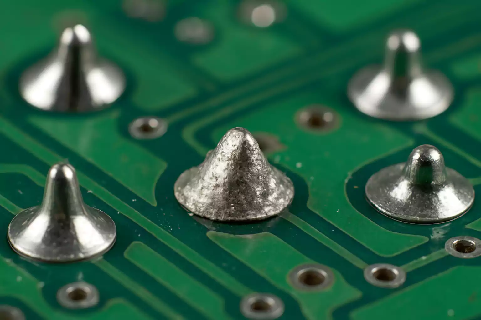
- Hidden solder joints are hard to inspect. BGA and PoP solder joints cannot be judged by visual inspection alone.
- Warpage can create unstable defects. Fine-pitch packages may suffer from open joints or head-in-pillow defects during reflow.
- Supplier communication becomes unclear. If the PoP stack, ball layout, and assembly process are not confirmed early, production risk increases.
A professional PCBA manufacturer reduces these risks by checking the package structure, SMT process, and inspection plan before mass production.
- For limited PCB space, we review whether PoP can reduce component footprint and improve layout efficiency.
- For crowded routing, we check ball pitch, escape routing, layer stack-up, and impedance requirements.
- For hidden solder joints, we use X-ray inspection and process control for BGA and PoP assembly.
- For warpage risk, we control baking, placement accuracy, flux or solder paste dipping, and reflow profiling.
- For unclear specifications, we confirm datasheets, top and bottom package compatibility, test requirements, and production notes before assembly.
EBest Circuit (Best Technology) provides PCB manufacturing and PCBA assembly services for compact, high-density, and advanced electronic products. Our engineering team supports SMT assembly, BGA assembly, X-ray inspection, functional testing, and turnkey PCBA assembly services. If your project involves PoP Package on Package, BGA, fine-pitch components, or high-density PCB assembly, you can send your Gerber files, BOM, placement file, and assembly requirements to sales@bestpcbs.com for engineering review.
What Is PoP Package on Package?
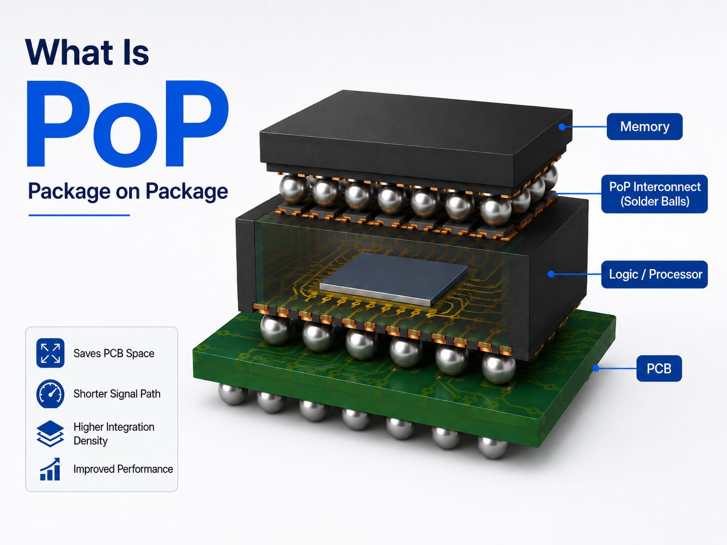
PoP Package on Package is a 3D IC packaging approach where two or more completed packages are vertically stacked. The most common combination is a bottom logic package and a top memory package. Instead of placing the processor and memory side by side on the PCB, PoP places them in a vertical structure.
In simple terms, PoP means “package stacked on package.”
A typical PoP stack looks like this:
| Layer | Typical Device | Main Function |
|---|---|---|
| Top Package | LPDDR, NAND Flash, Memory | Data storage |
| Bottom Package | Application Processor, SoC, Logic IC | Computing and control |
| PCB | Main circuit board | Electrical connection and system support |
This structure allows the designer to use the same PCB footprint for two functional blocks. For smartphones, wearable devices, compact modules, and portable electronics, this can be very valuable.
The main idea is simple:
Board area saving ≈ footprint of the top package if it were mounted separately − extra keep-out and routing margin
PoP does not remove all design complexity, but it gives engineers a practical way to increase system integration without enlarging the PCB. That is why engineers, buyers, and product developers often study PoP when they want to understand how compact electronics achieve higher performance in limited space.
In short, PoP Package on Package is not just a packaging name. It is a space-saving and performance-oriented structure used when logic and memory need to work closely together.
How Does Package on Package PoP Work?
Package on Package PoP works by connecting the top package to the bottom package through solder balls, while the bottom package connects to the PCB through its own solder balls. The upper and lower packages are designed to match each other mechanically and electrically.
The bottom package usually has two connection interfaces:
- Bottom-side solder balls for connection to the PCB.
- Top-side pads or exposed connection points for connection to the upper memory package.
The top package has solder balls on its bottom side. During assembly, these balls are aligned with the top-side pads of the bottom package. After reflow soldering, the top and bottom packages become one stacked structure.
A simplified connection path looks like this:
| Connection Path | Purpose |
|---|---|
| Top memory package to bottom logic package | Data transfer |
| Bottom logic package to PCB | System connection |
| PCB routing to other circuits | Power, control, RF, I/O |
The most important feature is vertical interconnection. Traditional PCB design connects processor and memory through horizontal traces on the PCB. PoP shortens part of this path by stacking the packages vertically.
This brings several engineering benefits:
- Shorter processor-to-memory connection
- Smaller PCB footprint
- Higher system packaging density
- Flexible memory selection
- Better use of limited board space
However, PoP also increases assembly sensitivity. The solder balls between the top and bottom packages are hidden, and the final solder quality depends on package coplanarity, placement accuracy, flux activity, solder volume, and reflow temperature control.
So, package on package PoP works through a matched vertical interconnect system. It saves space, but it also requires careful design and controlled SMT assembly.
What Is PoP Package on Package Assembly?
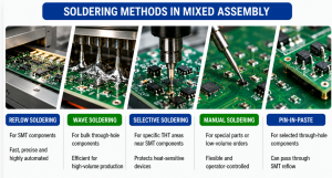
PoP Package on Package assembly is the SMT process used to mount the bottom package onto the PCB and then mount the top package onto the bottom package. It is closely related to the SMT PoP (Package on Package) process, which focuses on solder paste printing, component placement, flux or solder paste dipping, reflow soldering, and X-ray inspection.
In many PCBA factories, PoP assembly follows this general flow:
- PCB preparation
The PCB is checked for cleanliness, flatness, solder mask quality, and pad condition. - Solder paste printing
Solder paste is printed onto the PCB pads for the bottom PoP component. - Bottom package placement
The logic package or SoC is placed onto the PCB with high-precision SMT equipment. - Top package dipping
The memory package is dipped into flux or a controlled solder paste layer. - Top package placement
The top package is placed onto the bottom package with accurate alignment. - Reflow soldering
The full PoP stack passes through the reflow oven to form solder joints. - X-ray inspection
Hidden joints are inspected to check solder quality, alignment, voiding, and bridging. - Electrical and functional testing
The completed PCBA is tested based on the product requirement.
The key difference between ordinary BGA assembly and package on package pop assembly is that PoP has two soldering interfaces:
| Assembly Type | Soldering Interface |
|---|---|
| Standard BGA | BGA to PCB |
| PoP Assembly | Top package to bottom package + bottom package to PCB |
This means PoP assembly needs tighter process control than ordinary SMT mounting. The placement system must align both packages accurately, and the reflow profile must support the full stack without causing package warpage.
PoP Package on Package assembly is therefore not only about placing two packages together. It is a controlled PCBA process that combines fine-pitch SMT, BGA assembly, reflow profiling, and X-ray inspection.
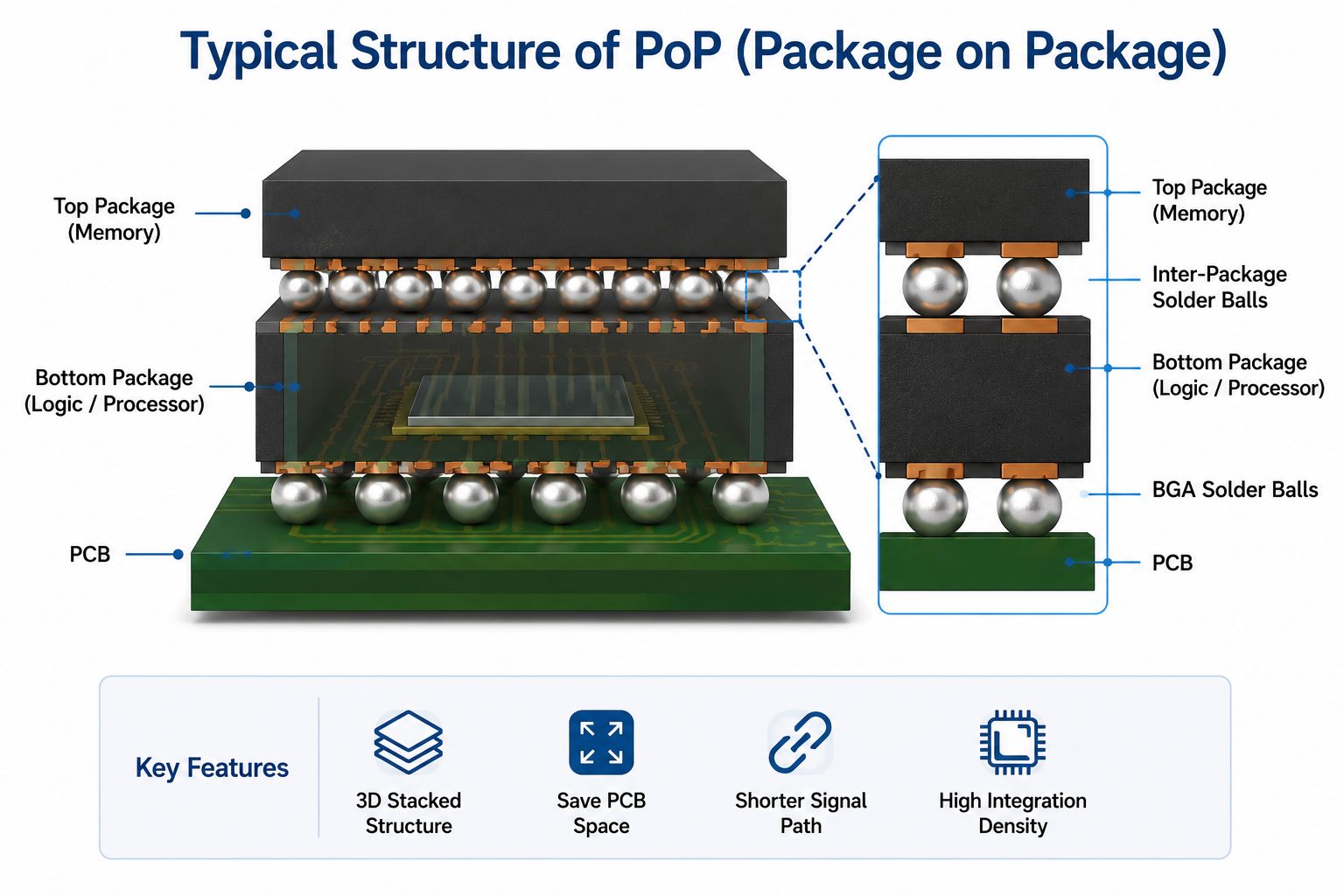
What Is the Typical Structure of PoP Package on Package?
The typical structure of PoP Package on Package includes a bottom logic package, a top memory package, solder balls between the two packages, and solder balls between the bottom package and the PCB. This vertical structure is the foundation of PoP technology.
A common PoP structure includes:
| Structure Part | Typical Role |
|---|---|
| Top Package | Memory or storage |
| Inter-package Solder Balls | Connection between top and bottom package |
| Bottom Package | Processor, SoC, or logic IC |
| Bottom BGA Balls | Connection to PCB |
| PCB Pads | Board-level electrical interface |
The bottom package is usually larger because it often contains the logic IC, substrate routing, and top-side connection pads. The top package is commonly a memory device, but the exact structure depends on product design.
The structure can vary by application. Some designs use standard solder ball connected PoP. More advanced designs may use TMV, also known as through-mold via technology, to create a thinner and more compact package interface.
Common PoP structure types include:
- Solder Ball Connected PoP
The upper package connects to the lower package through solder balls. - TMV PoP
Through-mold vias expose connection points through the mold compound for top package attachment. - Folded PoP
Flexible circuit structures are folded to connect different package layers. - BVA PoP
Bond Via Array technology supports fine-pitch vertical interconnects. - Memory Stacked PoP
Multiple memory dies or memory packages are stacked for higher capacity.
The structure selected depends on package height, I/O count, cost target, signal performance, and manufacturing capability.
In short, the typical PoP Package on Package structure is built around one main purpose: placing logic and memory into a compact vertical package system while keeping each package manufacturable and testable.
How Does the Ball Grid Work in PoP Package on Package?
The ball grid in PoP Package on Package provides the electrical and mechanical connection between the stacked packages and the PCB. In a standard BGA, the ball grid connects one package to the board. In PoP, the ball grid may connect both the bottom package to the PCB and the top package to the bottom package.
A PoP design may include two ball-grid levels:
| Ball Grid Position | Function |
|---|---|
| Top-to-bottom package balls | Connect memory to logic |
| Bottom-to-PCB balls | Connect logic package to PCB |
The ball grid must support electrical performance, mechanical stability, and manufacturability. If the grid is too dense, PCB escape routing becomes difficult. If the ball pitch is too small, soldering and inspection become more demanding.
Important ball-grid factors include:
- Ball pitch
- Ball diameter
- Pad size
- Solder mask opening
- Coplanarity
- Warpage behavior
- Reflow compatibility
In fine-pitch PoP packages, solder balls are often discussed in micron-level dimensions. Engineers may review ball diameter, standoff height, and solder joint reliability when checking package compatibility and assembly risk.
A useful way to think about PoP ball-grid risk is:
Smaller pitch + larger package size + higher warpage = higher assembly difficulty
This does not mean smaller pitch should be avoided. It means that process control must match the package requirement.
The ball grid is one of the most important parts of PoP Package on Package because it directly affects electrical connection, solder reliability, inspection difficulty, and PCB layout feasibility.
What Should Engineers Know About PoP Ball Layout?
PoP ball layout refers to the arrangement of solder balls and pads used to connect the top package, bottom package, and PCB. It affects routing density, signal integrity, solder reliability, and production yield.
For engineers and buyers, the practical question is clear: can the PCB and SMT PCB assembly process support this package safely?
Before production, engineers should check these key items:
- Ball pitch
Fine pitch improves density but increases routing and assembly difficulty. - Escape routing
The PCB must have enough layer count and trace width/spacing capability to route signals out from the BGA area. - Pad design
Pad size, solder mask defined pads, and non-solder mask defined pads must follow package recommendations. - Solder mask registration
Misregistration can reduce solder joint quality or create bridging risk. - Power and ground ball placement
Good power and ground distribution helps signal return paths and power integrity. - High-speed signal grouping
Memory signals should be routed with controlled length, impedance, and return path planning. - Keep-out area
The package area must leave enough space for assembly tolerance and inspection needs.
A compact comparison is shown below:
| Design Item | Why It Matters |
|---|---|
| Ball Pitch | Controls density and difficulty |
| Pad Design | Affects solder quality |
| Escape Routing | Decides PCB layer need |
| Power/Ground Balls | Supports stability |
| Warpage Margin | Reduces open-joint risk |
A good PoP ball layout is not only a package drawing. It is a manufacturing guide. If the layout is not reviewed before PCB fabrication, problems may appear during PCB SMT assembly, X-ray inspection, or functional testing.
In short, PoP ball layout connects packaging design with real PCBA manufacturability.
How Does SMT Support High-Density PoP Package-on-Package Assembly?
SMT supports high-density PoP Package-on-Package assembly by providing accurate solder paste printing, fine-pitch placement, controlled dipping, stable reflow soldering, and X-ray inspection. Without a controlled SMT process, PoP packaging cannot deliver its expected space-saving and performance benefits.
Advanced PoP structures may use finer pitches, smaller solder joints, thinner package bodies, and TMV through-mold via technology. SMT assembly must be able to handle these features consistently.
The production side usually focuses on these process controls:
- Stencil design
Aperture size and solder paste volume must match the bottom package pad design. - Solder paste selection
Paste type should support fine-pitch printing and stable reflow behavior. - Flux or solder paste dipping
The top package may need controlled dipping to support inter-package soldering. - Placement accuracy
Both top and bottom packages require precise alignment. - Reflow profile
Temperature ramp, soak, peak temperature, and cooling rate must be controlled. - X-ray inspection
Hidden solder joints must be inspected after reflow. - MSL control
Moisture-sensitive packages may require dry storage or baking before assembly.
For high-density PoP assembly, the process window can be narrow. A small placement shift, uneven solder paste deposit, or poor reflow profile may create hidden defects.
Common defects include:
- Head-in-pillow
- Solder bridging
- Open joints
- Insufficient solder
- Voids
- Package warpage
- Misalignment
The SMT process is therefore the bridge between the PoP package design and the final working PCBA. PoP Package on Package depends on strong packaging design, but it also depends on disciplined SMT execution.
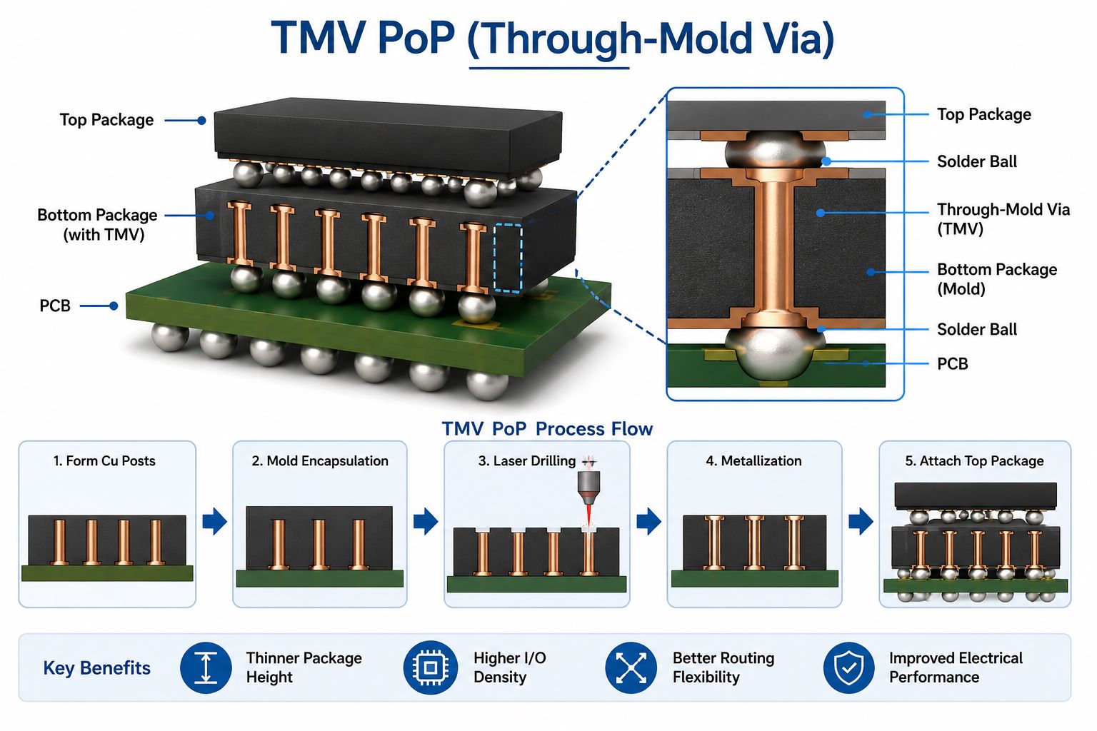
What Is TMV PoP with Through-Mold Vias?
TMV PoP with through-mold vias is an advanced PoP structure where vertical connection paths are formed through the mold compound of the bottom package. TMV stands for Through-Mold Via. This technology helps create thinner PoP structures and supports high-density vertical interconnection.
In a traditional solder ball connected PoP, the top package connects to solder balls or pads exposed on the bottom package. In TMV PoP, laser drilling or similar processes can expose vertical interconnect points through the molded package structure.
A simplified comparison:
| PoP Type | Connection Method | Main Benefit |
|---|---|---|
| Solder Ball PoP | Ball-to-pad connection | Mature and common |
| TMV PoP | Through-mold via connection | Thinner and denser |
| Folded PoP | Flexible circuit connection | Structure flexibility |
| BVA PoP | Bond via array | Fine-pitch interconnect |
TMV PoP is useful when the product requires:
- Lower package height
- Higher I/O density
- Better vertical integration
- Compact system design
- Improved package-level routing flexibility
However, TMV PoP also requires stronger control over package manufacturing and SMT assembly. The bottom package structure, exposed via quality, solder ball height, and top package alignment all affect final reliability.
For product teams, the key point is simple: TMV PoP can support more compact and advanced designs, but it should be reviewed early with both the package supplier and the PCBA manufacturer.
TMV PoP with through-mold vias is not just a thinner version of PoP. It is a packaging structure designed for higher-density electronic systems.
Where Is PoP Package on Package Used?
PoP Package on Package is mainly used in products that need high computing performance, compact PCB size, and short signal paths between logic and memory. It is common in mobile, portable, and miniaturized electronics.
Typical application areas include:
| Application | Why PoP Is Used |
|---|---|
| Smartphones | Saves space for processor and memory |
| Tablets | Supports compact system integration |
| Wearable Devices | Reduces PCB footprint |
| Camera Modules | Helps compact imaging electronics |
| IoT Devices | Supports small connected products |
| Portable Medical Devices | Saves internal space |
| Communication Modules | Improves integration density |
Smartphones are one of the most common examples. An application processor may be placed in the bottom package, while LPDDR memory is stacked on top. This allows the design to keep the processor and memory very close without using extra PCB area.
Wearable devices also benefit from PoP because the internal space is extremely limited. Smart watches, health monitoring devices, wireless earbuds, and compact sensor modules often need more functions in smaller product bodies.
PoP is also useful when the product needs fast communication between logic and memory. The shorter interconnect path can help reduce routing complexity compared with placing the components far apart on the PCB.
However, PoP is not suitable for every project. If the product has enough PCB area, low-speed requirements, or a cost-sensitive design, a side-by-side processor and memory layout may still be more practical.
PoP Package on Package is best used when space saving, high integration, and processor-memory proximity are more important than the extra assembly complexity.

FAQs about PoP Package on Package
Q1: What does PoP Package on Package mean?
PoP Package on Package means one IC package is stacked on top of another IC package. The most common structure is memory on top and a logic processor or SoC at the bottom.
Q2: Is PoP the same as BGA?
No. BGA is a package connection style using solder balls. PoP often uses BGA-style solder balls, but it is a stacked package structure, not just a single BGA package.
Q3: What is the difference between PoP and standard SMT assembly?
Standard SMT assembly mounts components onto the PCB. PoP assembly mounts the bottom package onto the PCB and also mounts the top package onto the bottom package.
Q4: Why is PoP used in smartphones?
PoP is used in smartphones because it saves PCB space, keeps memory close to the processor, and supports high-density system design.
Q5: What is package on package pop assembly?
Package on package pop assembly is the SMT assembly process used to build the stacked PoP structure. It includes solder paste printing, bottom package placement, top package dipping, top package placement, reflow soldering, and X-ray inspection.
Q6: Why is X-ray inspection important for PoP?
PoP solder joints are hidden under the packages and between package layers. X-ray inspection helps check solder bridging, open joints, voids, and alignment problems.
Q7: What are package on package pop assembly balls?
They are solder balls used to connect the top package to the bottom package and the bottom package to the PCB. Their size, pitch, and coplanarity directly affect assembly reliability.
Q8: What is TMV in PoP packaging?
TMV means Through-Mold Via. It is a vertical interconnect technology used in advanced PoP packages to support thinner and denser package structures.
Q9: Is PoP suitable for every PCB project?
No. PoP is most useful when PCB space is limited and high integration is required. For simple or low-cost products, standard side-by-side component placement may be enough.
Q10: What files should I provide for a PoP assembly quotation?
You should provide Gerber files, BOM, pick-and-place file, assembly drawing, datasheets for the top and bottom packages, and any special inspection or testing requirements.
To conclude, PoP Package on Package is a stacked IC packaging method that places one package on top of another to save PCB space, improve integration density, and support compact electronic system design. This article explained what PoP means, how package on package PoP works, how PoP assembly is handled, why ball grid and ball layout matter, how SMT supports high-density PoP production, and where TMV PoP is used.
For product teams, the main value of PoP is clear: it helps combine logic and memory in a smaller area while supporting modern compact electronics. But the process also requires accurate PCB design, compatible package selection, controlled SMT assembly, and reliable inspection.
EBest Circuit (Best Technology) supports high-density PCB manufacturing and PCBA assembly for products that use BGA, fine-pitch components, PoP Package on Package, and advanced SMT assembly. Our team can help review your PCB files, BOM, component package details, and inspection requirements before production.
For PoP Package on Package assembly support or PCBA quotation, please contact us at sales@bestpcbs.com.