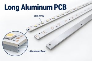
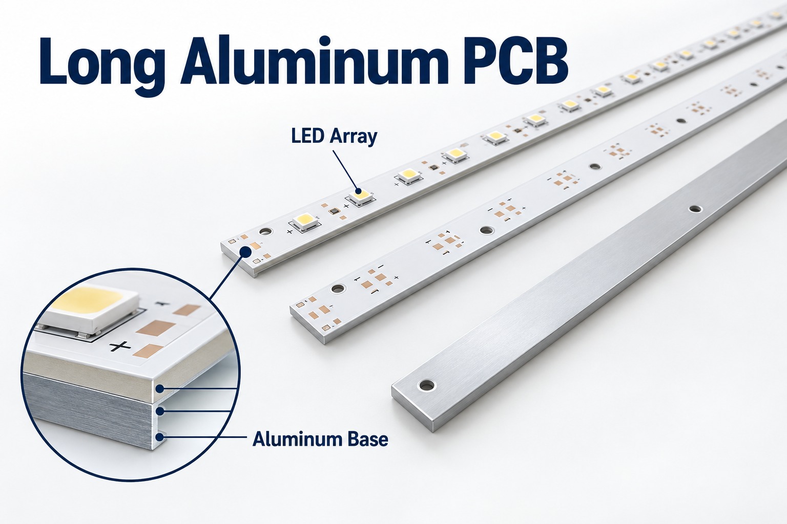
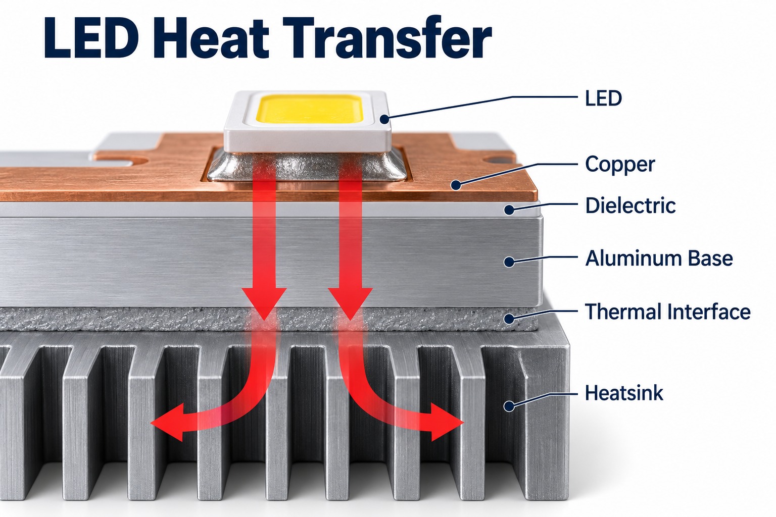
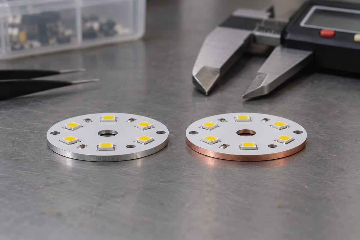
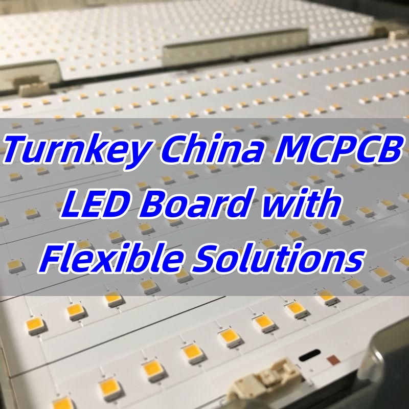
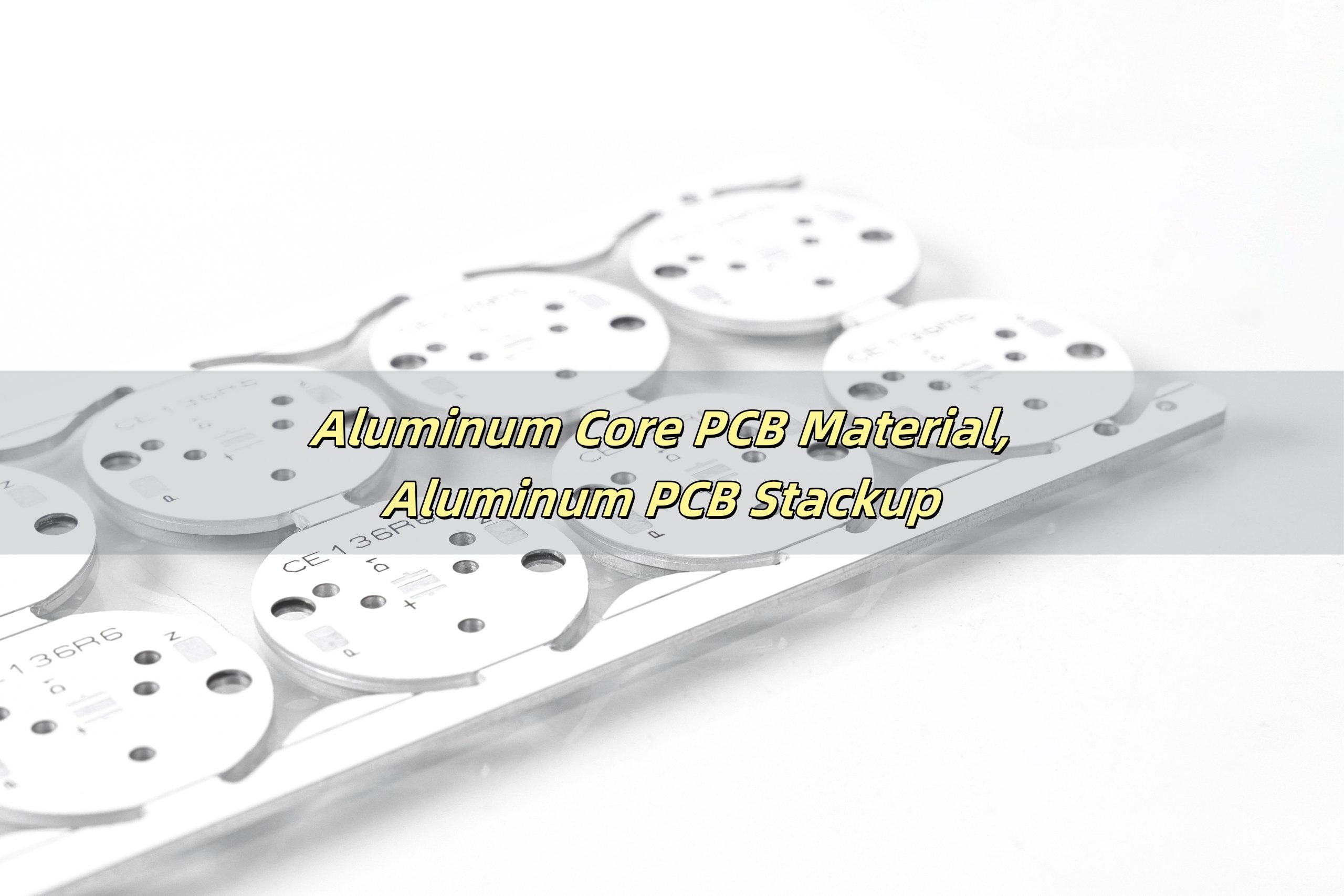
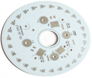
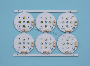
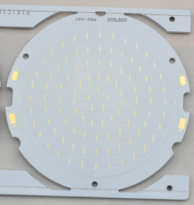
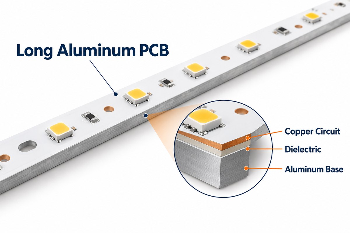
A long aluminum PCB is an elongated metal-core circuit board that carries an LED array and transfers heat toward the light fixture’s heatsink. Its copper circuit is separated from the aluminum base by a thermally conductive electrical insulation layer. For a 1.2-meter design, the main questions are usable manufacturing length, flatness after processing, and compatibility with the assembly line—not length alone.
At EBest Circuit, we support aluminum PCB fabrication, component sourcing and PCB assembly. Send your board drawing and thermal requirements for a DFM review before fixing the material or production layout.
Key Takeaways
- A long aluminum PCB combines electrical routing with a metal heat-spreading base for linear LED lighting.
- Our MCPCB capability table lists 480 × 1180 mm regular aluminum large-sheet dimensions and 1600 × 480 mm special single-sided processing. Finished-board and assembly dimensions require separate confirmation.
- A 1.2-meter strip needs an agreed flatness limit, measurement condition and heatsink mounting arrangement.
- Dielectric options include 1, 2 and 3 W/m·K grades. Thickness and thermal resistance matter alongside conductivity.
- Long-board process planning must address support, profiling, handling and soldering—not just the laminate size.
- Marine lighting requires coordinated moisture, corrosion and enclosure design. A bare PCB does not establish a luminaire’s environmental rating.
- Quote files should define the mechanical drawing, material, quantities and acceptance tests, with BOM and placement data for PCBA.
What Is a Long Aluminum PCB?
A long aluminum PCB is a rigid aluminum-based circuit board whose elongated shape suits a linear product, such as an LED light bar. “Long” describes the geometry; it is not a separate electrical technology or a standardized length class.
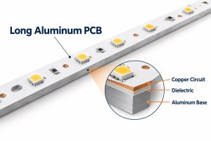
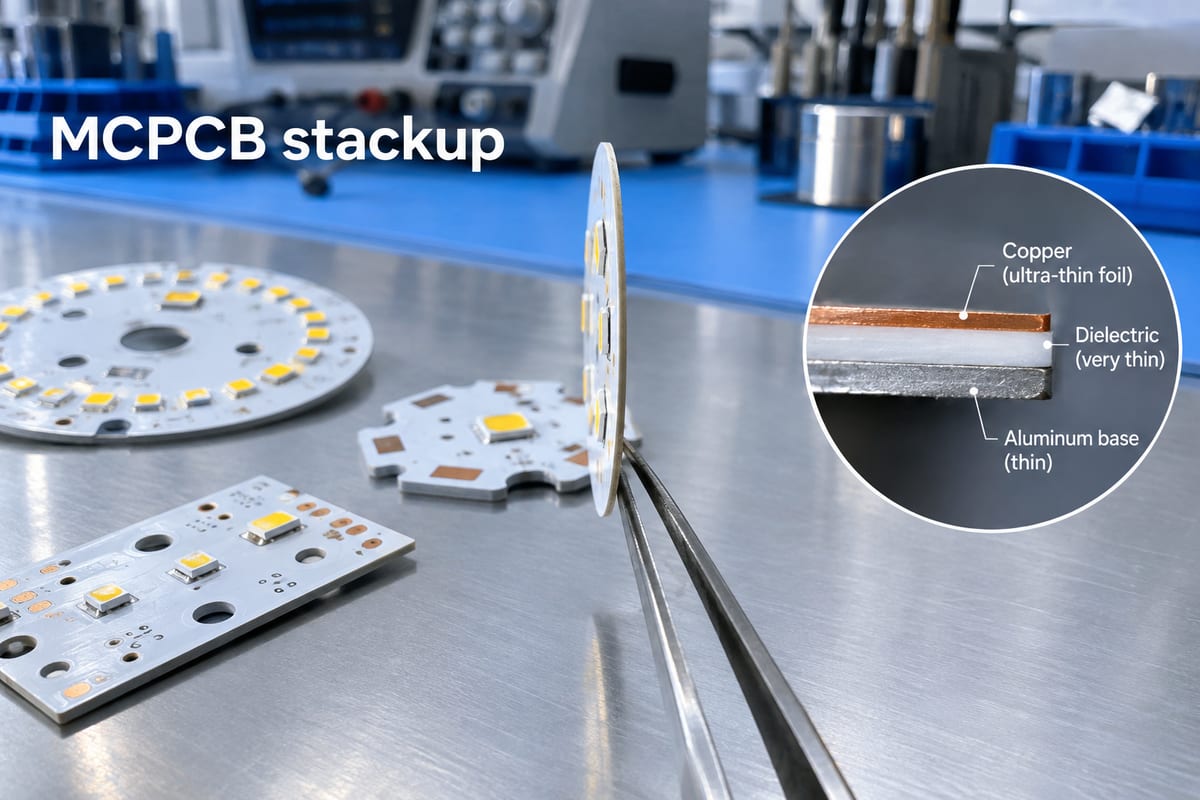
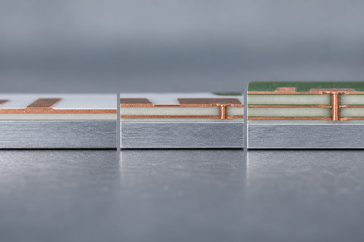
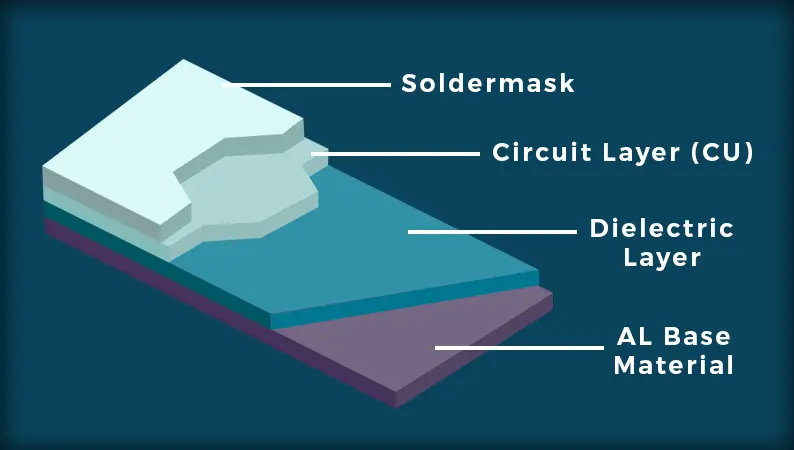
A typical single-sided aluminum PCB stackup contains these layers:
| Layer | Function |
| Copper circuit | Connects LEDs, resistors and power connections. |
| Thermally conductive dielectric | Electrically isolates the circuit from the metal while conducting heat. |
| Aluminum base | Supports the board and spreads heat toward the mounting surface. |
Solder mask covers the circuit except at exposed pads. Aluminum boards belong to the metal core PCB family; the metal base is not automatically an electrical ground connection.
Why Are Long Aluminum PCBs Used in LED Lighting?
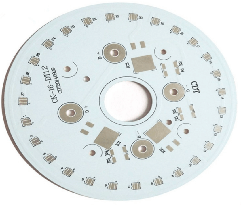
Long aluminum PCBs fit continuous LED rows while providing a heat-transfer path to a linear heatsink or housing. A single board can also reduce the number of connectors between shorter LED modules.
They suit architectural light bars, linear fixtures and selected marine lighting assemblies. The board supports LED placement along the optical path, but uniform brightness still depends on the driver, LED spacing, bin selection and optical design.
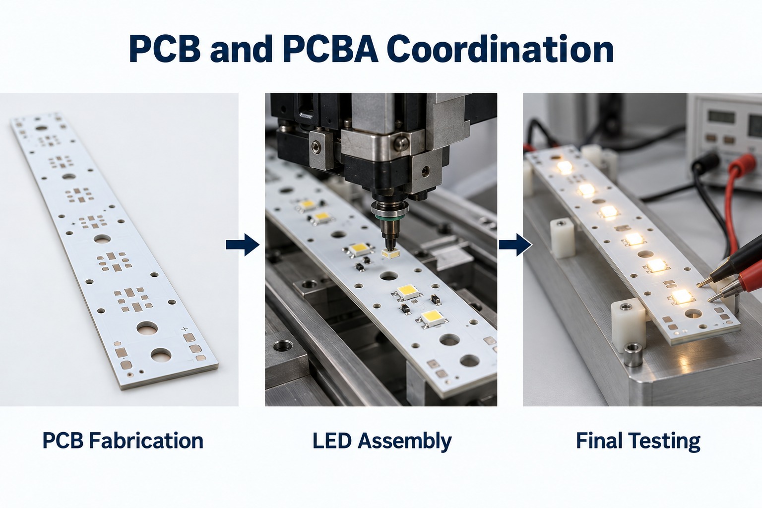
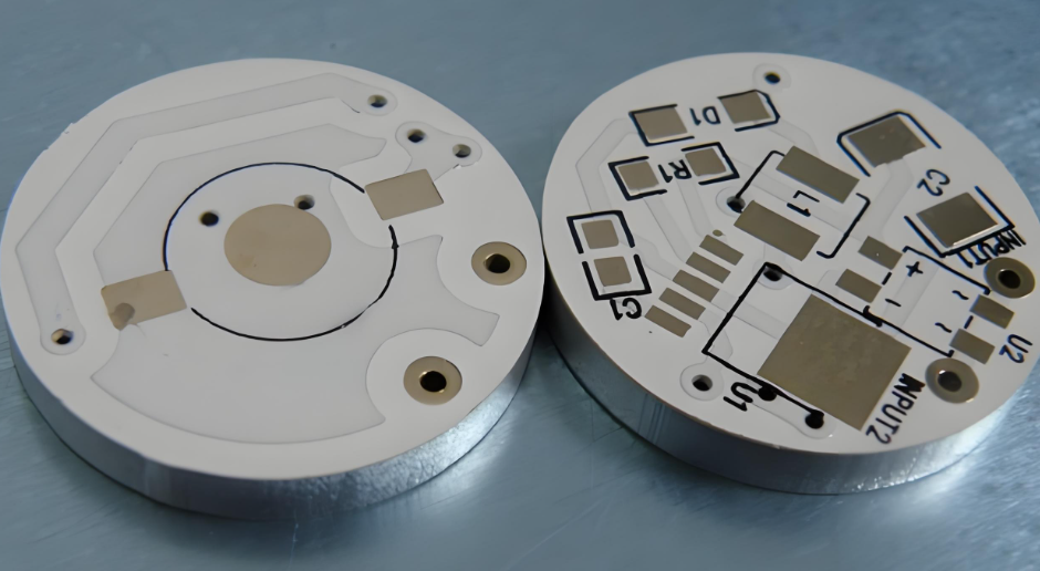
We can bring the aluminum light board and a separate FR-4 driver or control board into the same PCB/PCBA project. This lets the mechanical interfaces, connectors and test requirements be reviewed together. It does not require forcing a complex driver circuit onto the LED board.
How Long Can an Aluminum PCB Be?
Our MCPCB capability table lists 1600 × 480 mm for special single-sided aluminum processing, alongside a regular aluminum large-sheet size of 480 × 1180 mm. These figures describe different processing categories, not a blanket maximum for every finished board.
A 1200 mm finished strip exceeds the listed regular sheet length. It therefore needs a special-process review, including tooling space and the usable area remaining after manufacturing margins.
| Capability item | Listed range or condition |
| Regular aluminum large sheet | 480 × 1180 mm |
| Special single-sided aluminum processing | 1600 × 480 mm; project review required |
| Regular processing thickness | 0.8–3.0 mm |
| Thicker material | 4.0 and 5.0 mm by material order and confirmation |
| 1 oz copper line/space | 0.20/0.20 mm regular; 0.15/0.15 mm special |
These parameters are not guaranteed in every combination. Before releasing a long-board order, confirm three dimensions separately: the finished PCB, the fabrication panel, and the assembly carrier or panel. The printer, placement machine, reflow transport and inspection equipment each need to accommodate the approved format.
Why Is Flatness Difficult on a 1.2-Meter Aluminum PCB?
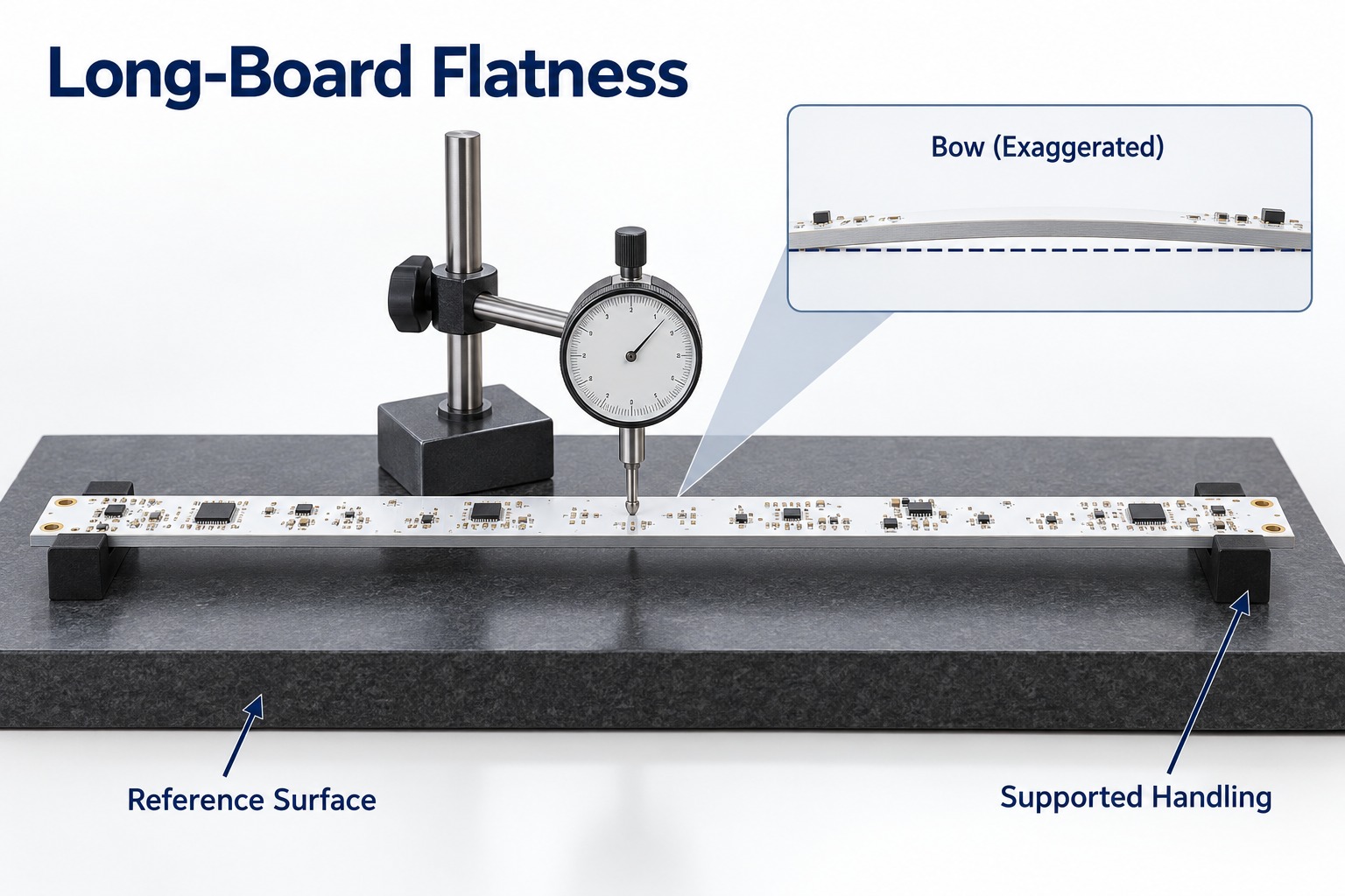
A 1.2-meter aluminum PCB makes small curvature more visible because the unsupported span is long. Its copper, dielectric and aluminum layers also respond differently to heating and cooling.
- Material and copper distribution: an asymmetric construction can develop uneven stress through processing.
- Thermal history: curing and soldering cycles can change the board’s free-state shape.
- Profiling and support: a narrow strip may move when it is separated from a larger panel.
- Handling and mounting: unsupported lifting or forcing the strip against uneven screw positions can introduce deformation.
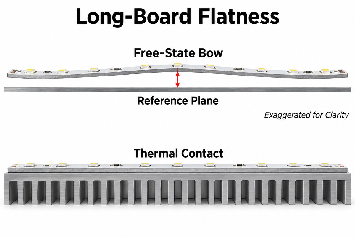
Specify flatness in the drawing with a measurement method. State whether the board is free or restrained, where it is supported, and whether inspection occurs before or after assembly. For illustration only, 0.5% of 1200 mm is 6 mm: a percentage that appears small can allow a large gap. This is not a recommended acceptance limit or an IPC test calculation.
How Do We Maintain Yield on Long, Narrow Aluminum PCBs?
Our starting point is a DFM review that connects the long-board layout with a practical fabrication and inspection plan. The detailed support method and process settings must be qualified for the selected design.
For long, narrow boards, the production review should resolve:
- Material and panel layout: confirm the selected laminate is available in the required usable size. Include tooling and handling margins.
- Support during processing: establish how the strip is held during machining, inspection and any assembly operation.
- Profile and hole quality: check edge clearances, mounting-hole positions and burr control against the drawing.
- First-article release: verify dimensions, flatness and electrical results before approving the production arrangement.
- Handling and packing: support the board along its length and prevent bending loads during transport.
For assembly, add stencil support and a soldering profile validated on the actual aluminum construction. Aluminum PCB design decisions should be reviewed before tooling is ordered; correcting a support or mounting problem after production starts adds rework. A meaningful yield figure must refer to a defined product and inspection plan, not an unrelated short-board run.
How Should You Choose Dielectric Thermal Conductivity for an LED Aluminum PCB?
Start by comparing the available 1, 2 and 3 W/m·K dielectric grades against the LED temperature budget, then check dielectric thickness and electrical insulation requirements. Our material table lists higher-conductivity 3–8 W/m·K options as requiring a material inquiry.
Aluminum PCB thermal conductivity is often quoted as the dielectric value—not the conductivity of the aluminum base or the complete board. Our listed regular dielectric thickness for specified material families is 100–110 µm; 150 and 200 µm options require confirmation.
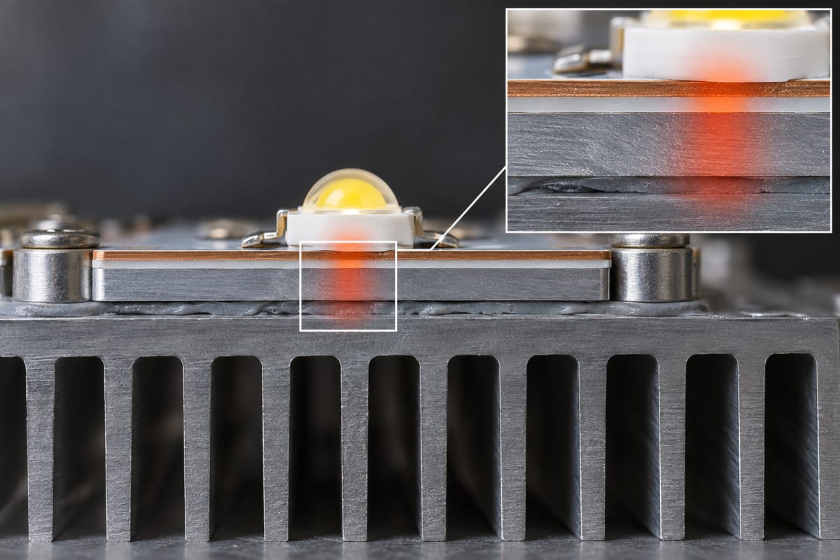
For an ideal uniform layer, thermal resistance is proportional to thickness divided by conductivity and heat-transfer area: R = t/(kA). At equal area, doubling conductivity halves that layer’s calculated resistance; doubling thickness cancels that benefit. The complete LED-to-ambient path also includes the package, solder connection, mounting interface and heatsink.
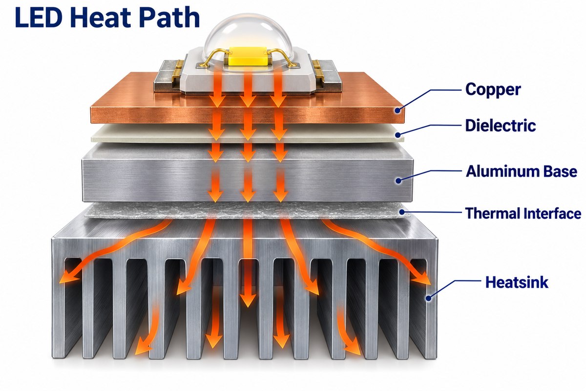
Request the exact laminate grade and its test method rather than comparing unlabeled conductivity numbers. Confirm insulation performance separately, and validate LED temperature in the intended housing at the specified operating current and ambient temperature. Higher conductivity alone does not establish an acceptable junction temperature.
What Should Be Checked for Marine LED Lighting PCBs?
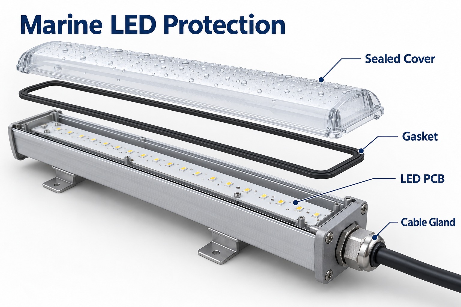
Marine LED lighting PCBs need checks for moisture exposure, corrosion paths and insulation, together with the luminaire’s sealing and heat-transfer design. Interior cabin lighting and an exposed exterior fixture do not face identical conditions.
- Water entry and condensation: define the expected exposure and how the enclosure, seals and cable entries manage it.
- Exposed metal: review board edges, mounting holes and dissimilar-metal contacts for the intended environment.
- Coating or potting: specify coverage and keep-outs for LEDs, connectors and heat-transfer surfaces; check material compatibility.
- Mechanical installation: assess mounting stress, vibration and connector strain relief.
- Electrical protection: define operating voltage, insulation requirements and the driver’s protection needs.
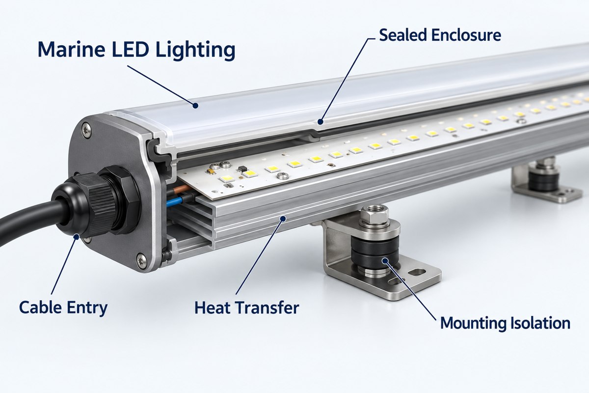
The qualification plan should identify tests for the PCB, PCBA and complete fixture separately. A coating on the board does not by itself establish an IP rating, and a company quality-system certificate is not marine product approval.
What Tests Are Important for Long Aluminum PCBs?
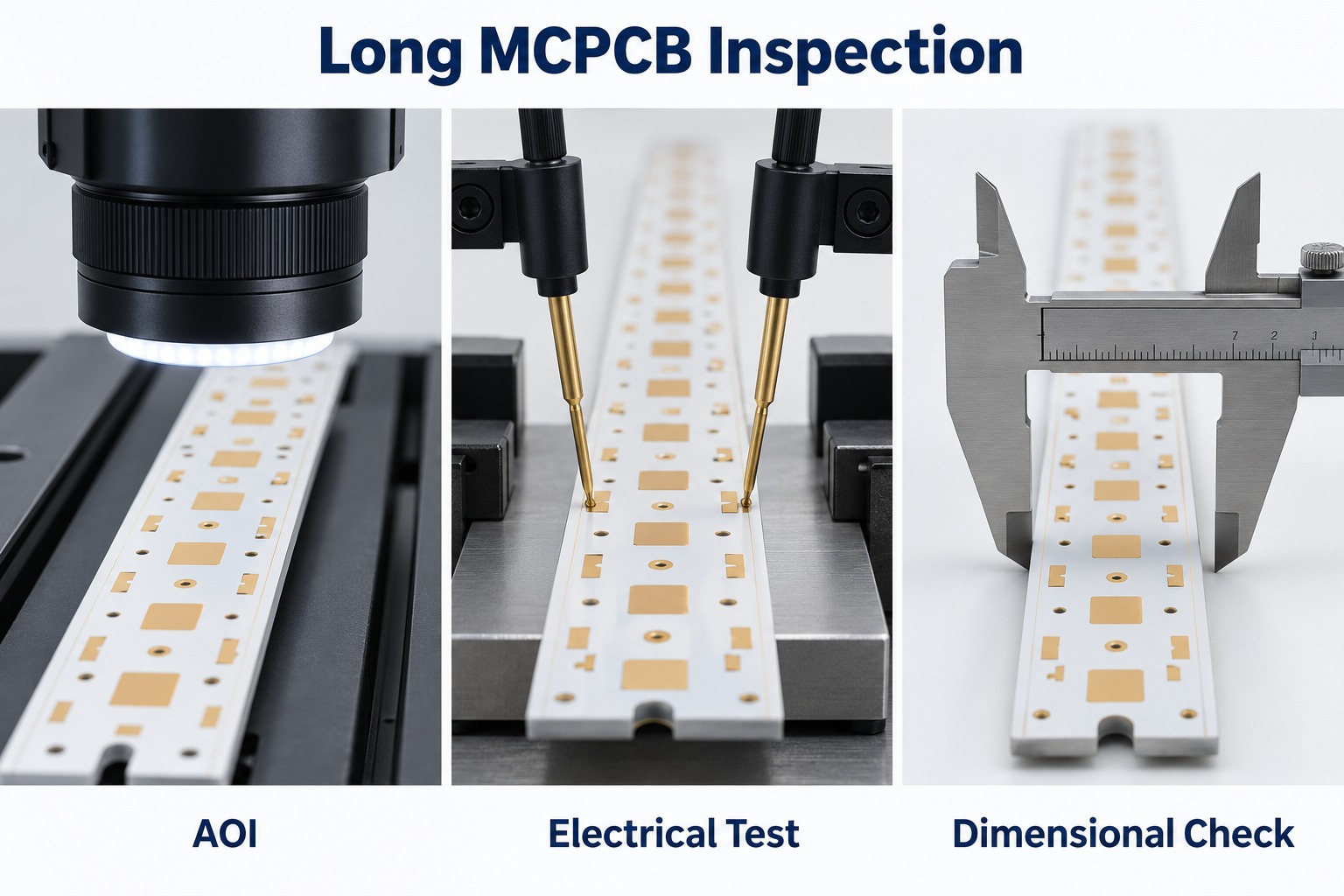
Long aluminum PCBs need dimensional and flatness checks plus electrical continuity and short-circuit testing. Assembled LED boards also need solder-joint inspection and the functional checks defined for the lighting circuit.
| Stage | Check | What it verifies |
| Bare PCB | Dimensions, holes and flatness | Fit against the released mechanical drawing |
| Bare PCB | Open/short electrical test | Circuit connectivity against approved data |
| PCB or PCBA, as specified | Insulation resistance or dielectric withstand | Insulation under the agreed test conditions |
| PCBA | Paste and solder inspection | Deposit quality, placement and inspectable solder joints |
| PCBA | Powered functional test | LED polarity, string operation and specified electrical behavior |
| Qualification build | Thermal and environmental validation | Performance in the defined installation and exposure |
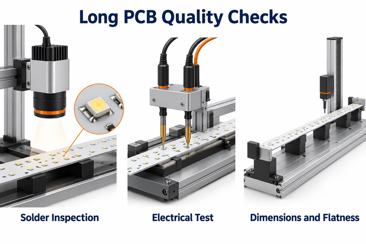
Our listed inspection resources include AOI, electrical testing, dimensional measurement, SPI, X-ray and functional testing. The selected methods, equipment size coverage and acceptance criteria must match the actual long-board project. X-ray is relevant where a joint cannot be assessed adequately by optical inspection; it is not a substitute for a functional test.
Agree the test voltage, duration, limits and sampling plan before ordering. Separate qualification tests from routine production tests so neither cost nor acceptance depends on an unstated assumption.
What Should Buyers Ask an Aluminum PCB Manufacturer?
Ask an aluminum PCB manufacturer to confirm the usable finished-board size and the corresponding assembly route in writing. A maximum sheet dimension alone does not answer whether your long LED strip can be built and tested.
- Which laminate grade, dielectric thickness and copper thickness are included in the quote?
- How will flatness be measured, and which limit applies after soldering?
- Which fabrication and assembly operations are in-house, and which need another facility or a special process?
- What first-article records and production test results will be supplied?
- What are the prototype and repeat-order quantities, lead times and tooling charges?
- How are approved material substitutions and LED bin requirements controlled?
- How will long strips be packed, and what purchasing commitments apply to forecast or stocked material?
Compare quotations using the same drawing revision and test scope. A lower bare-board price can conceal different material, inspection or packaging assumptions.
What Files Should You Send for an Aluminum PCB Quote?
Send fabrication data and a dimensioned drawing first; add the BOM, placement file and assembly drawing when you need a populated LED board.
- PCB data: Gerber or ODB++ files, drill data, outline and revision.
- Mechanical requirements: length, width, thickness, mounting holes, flatness limit and measurement condition.
- Material specification: laminate grade or required dielectric properties, copper thickness, solder mask and surface finish.
- Assembly data: manufacturer part numbers, approved alternatives, LED bin requirements, placement coordinates and polarity notes.
- Validation scope: electrical limits, functional test procedure and any thermal or environmental qualification requirements.
- Commercial information: prototype quantity, production lot sizes, forecast and required delivery schedule.
A heatsink or enclosure drawing is useful when board contact and mounting affect acceptance. Our PCB design guides provide additional background, but the released project drawing should define the actual requirements.
FAQ About Long Aluminum PCBs
Can a long aluminum PCB replace a flexible LED strip? Only where the installation accepts a rigid board. A conventional aluminum PCB cannot follow curves like a flexible strip, so the mechanical layout and mounting method may need to change.
Is white solder mask an electrical insulation layer? No. In the basic metal-core stackup, the specified dielectric isolates the copper circuit from the aluminum base. White solder mask covers the circuit surface and must not be treated as a replacement for that insulation.
Can LEDs and their driver use the same aluminum board? They can share a board if routing, insulation, thermal conditions and assembly access permit. A separate FR-4 driver board may be more practical when the driver requires more complex routing.
Does increasing aluminum thickness always solve overheating? No. It can change heat spreading and stiffness, but it does not remove resistance in the dielectric or a poor board-to-heatsink interface. Check the complete thermal path before changing thickness.
Can a long board be divided into shorter modules? Yes, if the optical and electrical design allows it. The trade-off is easier handling against additional interconnections, mechanical joints and possible gaps in the light pattern.
Why Choose EBest Circuit for Long Aluminum PCB and PCBA Projects?
We connect aluminum PCB fabrication with component sourcing and PCB assembly, so the light board, components and inspection requirements can be reviewed as one build. Our MCPCB capability table distinguishes regular materials and processing from special long-board requirements instead of treating every design as a standard panel.
For a new long-strip project, send the board drawing, Gerber files, material requirements and quantities to sales@bestpcbs.com. Include the BOM and test requirements if assembly is needed. We can then identify the engineering questions that must be resolved before prototype and production quotations are finalized.