An MCPCB stackup determines how heat leaves a component, how much current the circuit can carry, and how safely the copper remains isolated from the metal base. Selecting the stackup is therefore not a matter of choosing the highest thermal-conductivity material. It is a sequence of decisions about the heat path, electrical layers, dielectric, base metal, and cooling interface.
A useful starting rule is simple: use the least complex structure that meets the routing requirement, then improve the part of the thermal path that actually limits component temperature. This avoids paying for thicker metal, more layers, or a premium dielectric that does not address the real bottleneck.
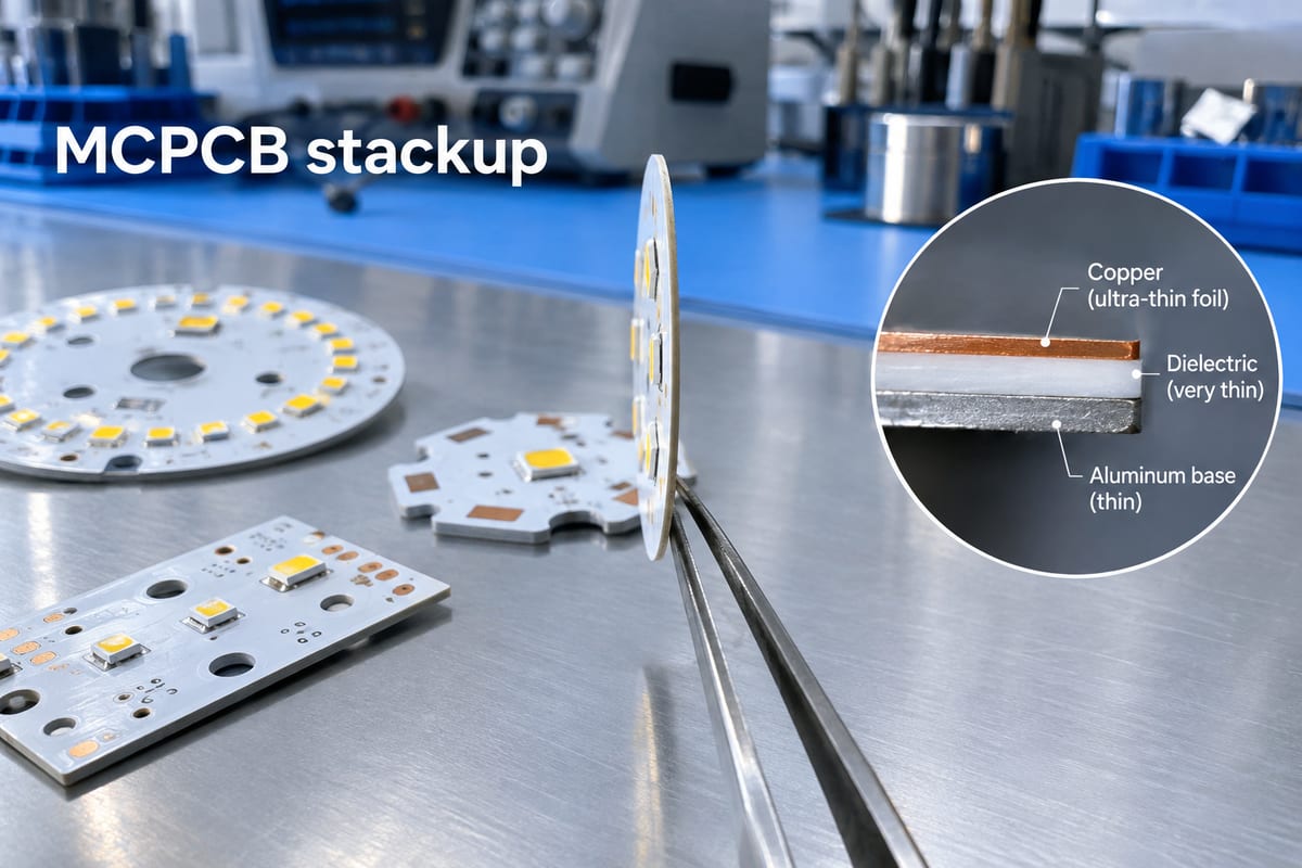
What Is an MCPCB Stackup?
An MCPCB stackup is the cross-sectional order and thickness of the board’s conductive, insulating, and metal layers. A conventional single-layer MCPCB contains:
- Copper circuit layer: forms traces and component pads and spreads heat laterally;
- Thermally conductive dielectric: transfers heat downward while electrically isolating the copper;
- Metal base: supports the board and spreads heat toward a heat sink, chassis, or enclosure.
These layers perform different jobs, so total board thickness alone does not define the design. A “1.5 mm aluminum PCB” could mean a 1.5 mm finished board or a 1.5 mm aluminum base plus copper and dielectric. It also says nothing about copper weight or dielectric thickness.
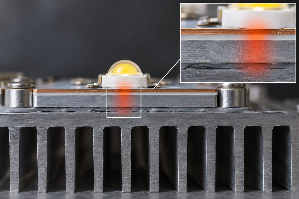
The stackup must be read as a complete heat path. Copper helps heat spread away from a small component pad. The dielectric controls much of the vertical resistance inside a conventional MCPCB. The metal base distributes heat over a wider area. The external cooling surface then removes that heat from the product.
This distinction explains why two boards with the same size and finished thickness can run at different temperatures. Their copper distribution, dielectric resistance, base material, or contact with the heat sink may be different.
How Does a Metal Core PCB Stackup Transfer Heat?
In a conventional metal core PCB stackup, heat normally travels through:
Component junction → package → solder or thermal pad → copper → dielectric → metal base → cooling interface → ambient air
Each stage adds thermal resistance. For a first-pass temperature estimate:
Temperature rise = Power × Total thermal resistance
If a device dissipates 10 W and the complete junction-to-ambient path is 4 °C/W, the expected temperature rise is approximately 40 °C above ambient. Reducing only the PCB dielectric resistance from 0.5 to 0.3 °C/W would lower that estimate by about 2 °C, not 20 °C. This prevents overestimating the benefit of one material upgrade.
Temperature measurements can help identify where the restriction lies:
- Hot component, much cooler metal base: resistance is likely concentrated near the package, pad, copper spreading area, or dielectric.
- Hot component and hot metal base, cooler heat sink: inspect the board-to-heat-sink interface.
- Component, base, and heat sink all hot: the external cooling system cannot reject enough heat.
- One local hotspot on an otherwise cool board: improve the local pad, copper spreading, or direct heat path before upgrading the whole board.
The decision is therefore not “Which metal conducts heat best?” It is “Which part of the junction-to-ambient path contributes enough resistance that changing it will materially lower temperature?”
Which MCPCB Structure Fits Your Application?
Choose the layer structure from the circuit requirement first, then verify that its heat path is short enough for the hottest components.
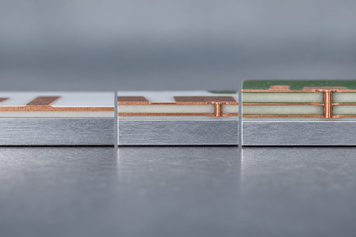
Use a single-layer MCPCB when all components and routing fit on one copper layer. It offers the shortest conventional path from the component pad through one dielectric layer to the metal base. This is often suitable for LED arrays, power modules, motor drives, and simple high-current circuits.
Move to a double-layer MCPCB when one layer cannot provide the required routing, ground plane, power distribution, or connector access. The second copper layer earns its place by solving an electrical problem. Heat from the upper layer may travel through vias or additional dielectric before reaching the base, so it is usually less direct.
Use a multilayer MCPCB when routing density, signal separation, power planes, or component placement requires more than two copper layers. Do not select it only because power is high; extra layers can increase rather than reduce the distance to the metal base.
A practical decision sequence is:
- Place the components and identify the devices that dominate heat generation.
- Check whether one copper layer can meet routing and current requirements.
- Add another layer only when a defined electrical constraint cannot be solved cleanly.
- Trace the heat path from each critical device to the metal base.
- If only one area has excessive heat density, compare a localized solution with increasing the complexity of the entire board.
For example, a 100 W LED assembly distributed across a large board may work well on a single-layer aluminum MCPCB. A 40 W power-control board with dense gate-drive and sensing circuits may require two or more copper layers even though its total power is lower. Total wattage alone does not determine the layer count.
How Do Aluminum and Copper Bases Affect Performance?
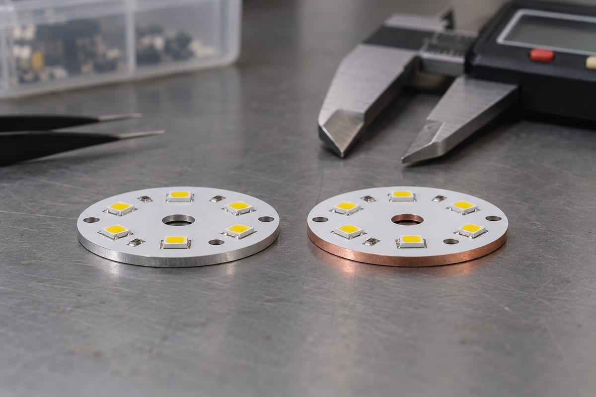
Choose aluminum when the base provides adequate heat spreading and weight or cost matters. Choose copper when heat is concentrated in a small area and spreading through the base is a significant part of the temperature rise.
Copper’s thermal conductivity is roughly higher than aluminum’s, so it can reduce temperature differences across the metal base. The benefit is greatest when heat must spread laterally from a small source before reaching a larger heat sink. It is smaller when heat already enters a large area or when the dielectric and external interface dominate total resistance.
Use these observations:
- Several devices create a hotspot near the center while the base edges remain cool: copper may improve lateral spreading.
- The whole aluminum base is nearly uniform but too hot: changing to copper is unlikely to solve insufficient external cooling.
- The component is hot while the aluminum directly beneath it is much cooler: improve the path through the pad, copper, or dielectric first.
- Product weight and material cost are sensitive: aluminum is normally the better starting point.
Base thickness follows a similar rule. Increasing thickness improves stiffness and gives heat more cross-sectional area for lateral spreading. It does not reduce the dielectric resistance, and it does not create additional cooling capacity. Once the base temperature is reasonably uniform, making it thicker usually produces diminishing thermal returns.
The choice should therefore be based on measured or modeled temperature distribution, not on the assumption that copper or a thicker base is automatically safer.
How Should You Select the Dielectric Layer?
Select the dielectric by setting an allowable thermal resistance first, then checking that the chosen thickness provides sufficient electrical isolation and reliability.
The approximate thermal resistance of the dielectric is:
Rθ = t ÷ (k × A)
where:
- t is dielectric thickness in meters;
- k is thermal conductivity in W/m·K;
- A is effective heat-transfer area in square meters.
Assume an effective area of 100 mm²:
- 100 μm at 3 W/m·K gives approximately 0.33 K/W;
- 75 μm at 2 W/m·K gives approximately 0.38 K/W.
Although the first material has 50% higher conductivity, its calculated layer resistance is only slightly lower because it is also thicker. This is why comparing W/m·K alone can be misleading. The calculation is illustrative and excludes package, solder, copper-spreading, contact, and heat-sink resistance.
Use this selection order:
- Estimate how much of the total temperature rise can be allocated to the dielectric.
- Compare candidate materials using conductivity, actual thickness, and effective pad area.
- Eliminate options that do not provide adequate isolation for operating voltage, transients, tolerances, and environment.
- Check adhesion, soldering exposure, thermal cycling, moisture, and aging requirements.
- Confirm with thermal modeling or a prototype only when the remaining margin is too small for a first-order estimate.
The correct action depends on the bottleneck:
- If dielectric resistance is too high but isolation margin is generous, reducing thickness may be effective.
- If thickness cannot be reduced safely, use a higher-conductivity dielectric or increase the heat-transfer area.
- If the entire metal base is already hot, improving the dielectric will have limited value; improve the external cooling path.
- If one small pad is hot, enlarge the copper area or use a localized thermal structure before upgrading the dielectric across the whole board.
When Do You Need a Double Layer MCPCB or Multilayer MCPCB?
A Double Layer MCPCB is justified when the second copper layer solves a specific electrical-layout problem. A Multilayer MCPCB is justified when additional routing layers or planes are necessary. The thermal design must then be adapted to the longer and more complex path.
Consider a component on the top copper of a two-layer construction. Its heat may spread in the top copper, move through thermal vias to a lower copper layer, cross the dielectric, and enter the metal base. The vias reduce part of the vertical resistance, but they do not make the path identical to a single-layer MCPCB.
The layer choice changes these factors:
- Routing capacity: improves as copper layers are added.
- Vertical heat distance: may increase when more dielectric separates the component from the metal.
- Via dependence: increases when heat and current must move between layers.
- Copper balance: becomes more important for flatness and consistent heat spreading.
- Thickness and mass: generally increase with additional layers.
If the circuit needs only one or two local crossovers, redesigning the routing may be better than adding a complete layer. If a dense control circuit requires planes and signal separation across the board, the extra layers have clear value.
When one or two devices dominate the heat load, keep the required electrical layers but compare local thermal vias, direct thermal path, copper inserts, or ceramic beneath those devices. This separates the routing problem from the hotspot problem instead of forcing one structure to solve both inefficiently.
Which Stackup Details Should Your Fabrication Drawing Define?
The drawing should show enough cross-sectional information to distinguish the intended MCPCB from every plausible alternative.
At minimum, show:
- each copper layer and its finished thickness;
- each dielectric layer and its thickness;
- metal type and metal-base thickness;
- total finished board thickness;
- the position of the metal relative to all copper layers;
- vias, insulated holes, exposed metal, or direct thermal features that change the heat path.
Avoid one-line descriptions that combine several dimensions. Instead of “1.5 mm aluminum PCB, 2 oz copper,” separate the structure:
70 μm finished copper / 100 μm dielectric / 1.5 mm aluminum base
This shows immediately that the base is 1.5 mm and the total finished board will be thicker. If 1.5 mm is intended as the overall thickness, the base must be adjusted accordingly.
For multilayer structures, draw each copper and dielectric layer in order and show which vias connect them. If a hole passes through the metal, show the insulating clearance around it. If a component uses a direct thermal path, show where the thermal pad contacts metal and where electrical isolation remains.
Also separate material properties from product targets. A dielectric conductivity value defines one layer. A maximum component temperature under a stated power and cooling condition defines the expected outcome. Both are useful, but neither can substitute for the other.
How Do Stackup Choices Affect Cost and Lead Time?
Stackup cost and lead time rise when a choice adds expensive material, less available material, or additional processing steps. The largest increase usually comes from combinations of changes rather than one specification alone.
The direction of each effect is predictable:
- Aluminum to copper: raises material cost and weight; the benefit is strongest for concentrated heat spreading.
- Standard to uncommon dielectric: may add sourcing time; use it when the thermal or insulation margin requires it.
- Standard to heavy copper: increases imaging and etching difficulty and may require wider spacing.
- Single layer to multilayer: adds lamination, drilling, plating, and alignment operations.
- Conventional to direct thermal path or copper insert: adds localized processing but may solve a hotspot that bulk material upgrades cannot.
- Common to tightly controlled thickness: reduces the available material and process window.
Use a value-based comparison rather than selecting the lowest board price. Suppose a copper base adds cost but lowers the critical device temperature by only 1 °C because the dielectric is the main resistance. That upgrade has poor value. If the same change lowers a concentrated hotspot enough to remove a larger heat sink, it may reduce total product cost.
Lead time follows material and process readiness. A common single-layer aluminum stackup has fewer dependencies. A multilayer copper-base construction with a special dielectric, heavy copper, and insulated metal-core holes combines several dependencies and will usually take longer.
The best-value stackup is the least complex one that meets the electrical limits and thermal target without paying for improvements outside the real bottleneck.
FAQs About MCPCB Stackup
Is every metal core PCB an aluminum PCB?
No. Aluminum is the most common base, but copper and specialized metal structures are also used. The choice depends on heat concentration, weight, cost, and the external cooling design.
Does higher dielectric conductivity always make the board cooler?
No. Actual layer resistance also depends on dielectric thickness and effective heat-transfer area. Package, solder, copper spreading, base metal, and cooling-interface resistance may dominate the result.
Does a thicker metal base always improve cooling?
No. It improves stiffness and lateral heat spreading, but it cannot compensate for a restrictive dielectric or inadequate external cooling. Once the base temperature is nearly uniform, additional thickness gives diminishing thermal benefit.
When is copper better than aluminum?
Copper is most useful when heat is concentrated and temperature varies significantly across the metal base. If the entire base is already uniformly hot, the external cooling system is the more likely limitation.
Can thermal vias improve an MCPCB stackup?
Yes, in double-layer and multilayer structures. They can connect copper areas and shorten part of the vertical path. Their effect depends on quantity, diameter, copper plating, placement, and the remaining dielectric-to-metal path.
Can one stackup support different power levels?
Yes. Power is only one input. Heat-source area, duty cycle, ambient temperature, airflow, enclosure, cooling contact, and allowable component temperature also determine whether the stackup works.
Need help comparing two MCPCB stackup options? Send the cross-sections, power dissipation, voltage, thermal target, and cooling conditions to sales@bestpcbs.com.
You may also like






Tags: Aluminum PCB Stackup, MCPCB Stackup, metal core pcb stackup