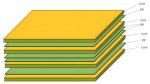
A PCB board stackup defines how copper and dielectric layers are arranged inside a printed circuit board. It determines where signals, ground references, and power distribution are placed, while also affecting impedance, EMI performance, board thickness, and fabrication cost.
Choosing a stackup is not simply a matter of selecting 2, 4, 6, or 8 layers. The structure must support the actual routing density, component packages, power rails, signal speeds, and mechanical requirements of the product. A well-planned 4-layer board may outperform a poorly arranged 6-layer design.
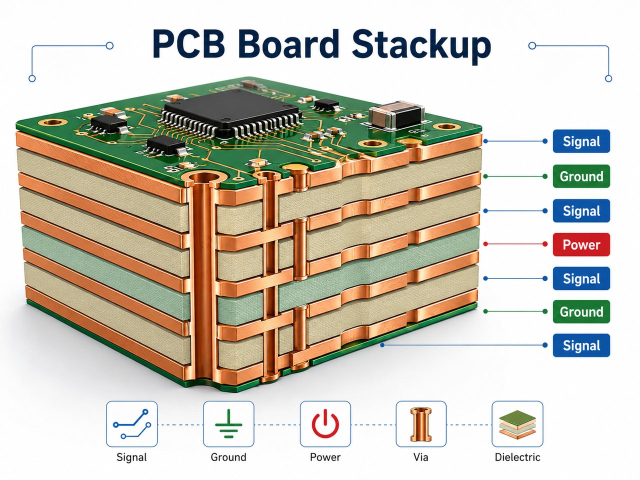
What Is a PCB Board Stackup?
A PCB board stackup is the vertical construction of copper layers, cores, and prepregs within a circuit board. Each copper layer may be assigned to signals, ground, power, or a combination of these functions.
A complete stackup usually specifies:
- Layer order and function
- Core and prepreg materials
- Dielectric thickness between copper layers
- Inner and outer copper weight
- Finished board thickness
- Controlled impedance requirements
The terms PCB stack up, PCB board layer stackup, and PCB board stack generally describe the same structure.
A basic 4-layer board may use L1 for signals, L2 for ground, L3 for power, and L4 for signals. However, this layer sequence alone is not enough for fabrication. Electrical performance also depends on dielectric thickness, material Dk, copper thickness, and trace geometry.
What Is the Difference Between PCB Layer Count and PCB Stackup?
PCB layer count states how many conductive copper layers are present. PCB stackup defines how those layers are arranged and separated.
| Item | PCB Layer Count | PCB Stackup |
|---|---|---|
| Main definition | Number of copper layers | Complete vertical board construction |
| Identifies layer function | No | Yes |
| Includes core and prepreg | No | Yes |
| Includes dielectric spacing | No | Yes |
| Supports impedance calculation | No | Yes |
| Used for lamination planning | No | Yes |
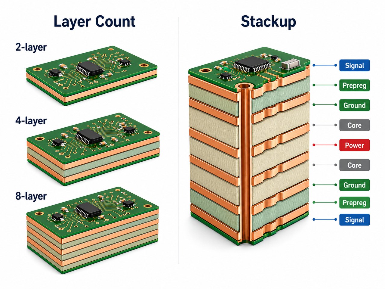
Two PCBs may both have 4 copper layers but behave differently because their dielectric spacing, copper weight, and reference-plane arrangement are not the same.
For example, “4 layers, 1.6 mm thick” provides only basic quotation information. A more useful specification would include L2 as ground, L3 as power, 1 oz finished outer copper, 0.5 oz inner copper, FR-4 Tg170, and a defined 50-ohm impedance structure. The manufacturer can then select real core and prepreg combinations instead of estimating from layer count alone.
How Do You Decide How Many PCB Layers You Need?
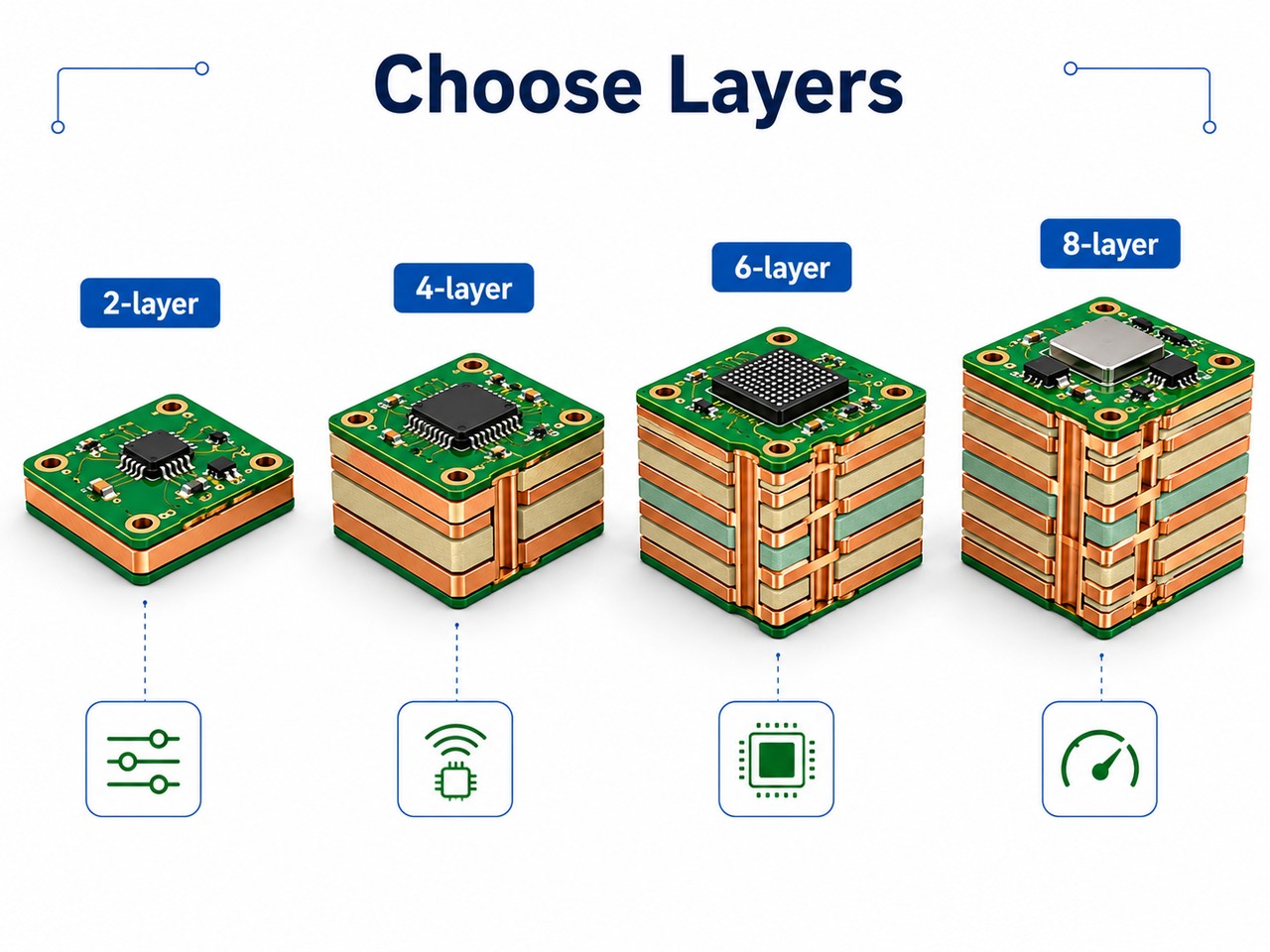
The correct layer count is the lowest number that provides enough routing space, reference planes, power distribution, and manufacturing margin.
| Layer Count | Typical Applications | Main Limitation |
|---|---|---|
| 2 layers | Basic controllers, relay boards, simple power supplies | Limited routing space and less continuous ground coverage |
| 4 layers | MCU boards, IoT devices, industrial controls, communication modules | May become restrictive with dense BGAs or many power rails |
| 6 layers | Mixed-signal systems, moderate BGA density, several high-speed interfaces | Higher cost than 4 layers |
| 8 layers | FPGA, DDR, high-speed communication, complex power systems | Requires more detailed stackup and impedance planning |
Routing density: More layers may be justified when traces require excessive detours, narrow spacing, or many vias. Increasing the PCB board size can create more routing area, but enclosure dimensions may not allow it.
Component packaging: Fine-pitch BGAs often determine the minimum practical layer count. Fan-out style, via diameter, pitch, and the number of signal rows all affect how many routing layers are required.
Signal speed: USB, Ethernet, HDMI, PCIe, and DDR interfaces benefit from continuous reference planes and controlled dielectric spacing. These interfaces can be difficult to manage on a 2-layer PCB even when the component count is modest.
Power distribution: A design with several voltage rails may require dedicated power regions or planes. A board with only 1 or 2 low-current rails may distribute power through traces and copper pours instead.
EMI and compliance: Adding ground planes can reduce loop area and improve return-path continuity, which becomes more valuable when the product must pass formal EMC testing.
Do not add layers only because a board contains a fast processor. Review the actual interfaces, package fan-out, routing channels, and reference requirements first.
How Should Signal, Ground, and Power Layers Be Arranged?
Critical signal layers should normally sit next to continuous reference planes. Ground is usually the preferred reference because it is less likely to be divided into isolated voltage regions.
Keep fast signals close to a reference plane. A short dielectric distance confines more of the electromagnetic field between the trace and its reference. This improves impedance control and reduces field spreading.
Avoid routing across plane splits. When a trace crosses a gap in its reference plane, return current must travel around the opening. The resulting loop can increase radiation, noise, and susceptibility.
Separate dense signal layers where possible. Two adjacent signal layers can couple through the dielectric, especially when long traces run in parallel. Placing a reference plane between them is usually preferable.
Keep power and ground close when the layer budget allows. A closely spaced power-ground pair provides plane capacitance and a compact current path. Local decoupling capacitors are still required at device power pins.
Maintain a balanced physical construction. Copper weight and dielectric thickness should be reasonably symmetrical around the center of the board. Large differences between the upper and lower halves can contribute to bow and twist.
What Is the Best 4-Layer PCB Stackup for Different Designs?
There is no single best 4-layer PCB stackup. The choice depends mainly on power complexity, routing space, and whether both outer signal layers require a solid ground reference.
| 4-Layer Structure | Suitable For | Main Trade-Off |
|---|---|---|
| Signal / Ground / Power / Signal | General embedded and industrial boards | Bottom-layer signals may reference a divided power plane |
| Signal + Power / Ground / Ground / Signal + Power | Designs prioritizing EMI control and ground continuity | Power routing consumes outer-layer space |
| Signal / Ground / Signal + Power / Ground | Mostly top-side assembly or specialized routing | Requires careful balance and reference-path review |
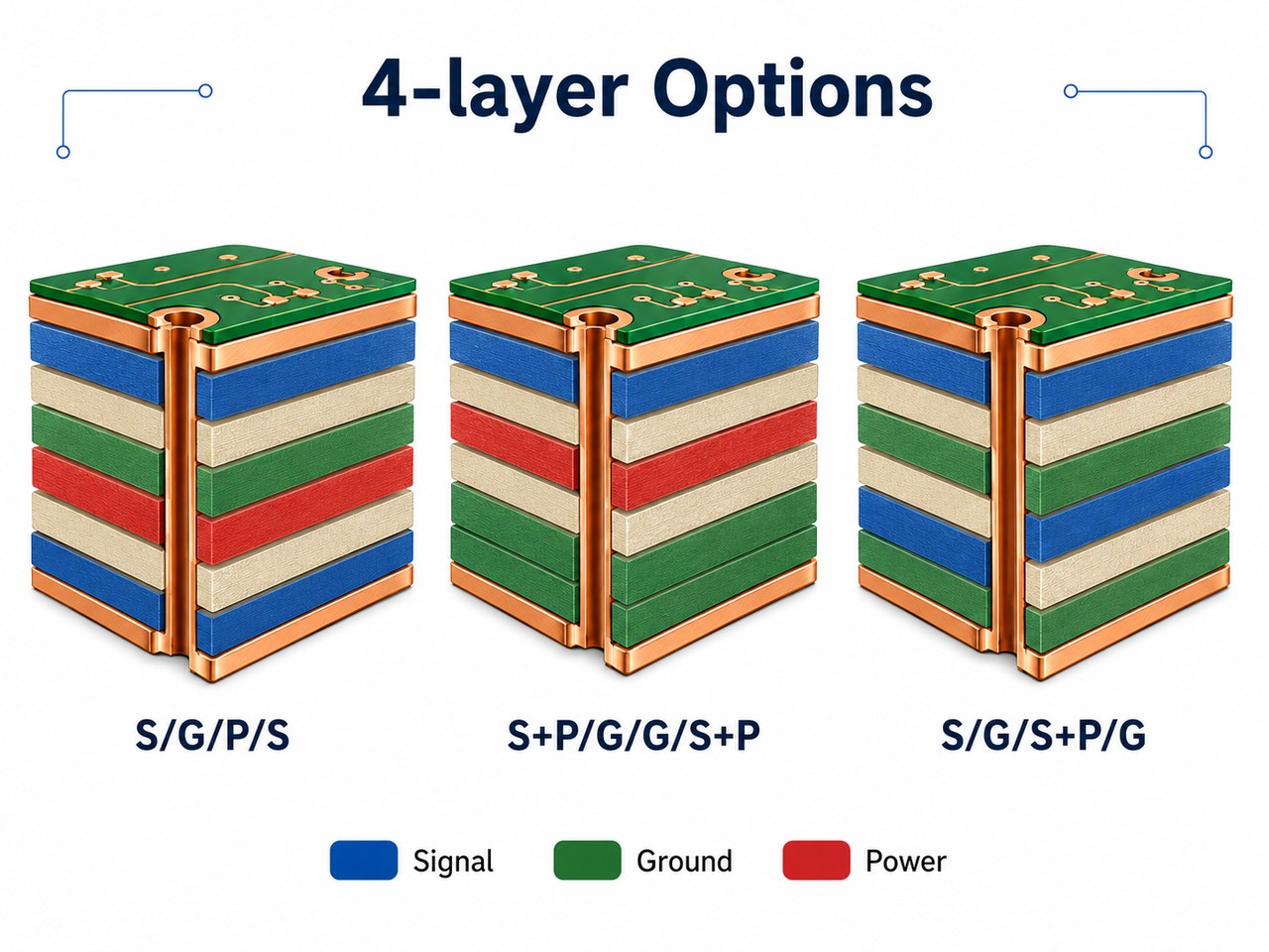
Signal / Ground / Power / Signal: This conventional structure works well when the board has several power rails, most critical traces stay on L1, and bottom-layer signals do not cross gaps in the L3 power plane.
Signal + Power / Ground / Ground / Signal + Power: Both outer layers receive a nearby ground reference. It is practical when the design has few power rails and EMI performance matters more than having a dedicated power plane.
Signal / Ground / Signal + Power / Ground: This arrangement may suit a board with most components on the top side. It is a specialized option, so the L3 reference relationship, copper balance, placement, and lamination structure require careful review.
For many general-purpose products, Signal–Ground–Power–Signal remains a practical starting point. For designs with simple power distribution and tighter EMI targets, a dual-ground structure may provide better return-path control.
What Is a Practical 8-Layer PCB Stackup Example?
An 8-layer PCB stackup example should be selected according to signal-layer demand, power rails, and package fan-out. Copying a generic template without checking the routing plan can waste layers or create poor reference relationships.
| Layer | Function |
|---|---|
| L1 | Components and high-speed signals |
| L2 | Ground plane |
| L3 | Signal |
| L4 | Ground plane |
| L5 | Power plane |
| L6 | Signal |
| L7 | Ground plane |
| L8 | Components and signals |
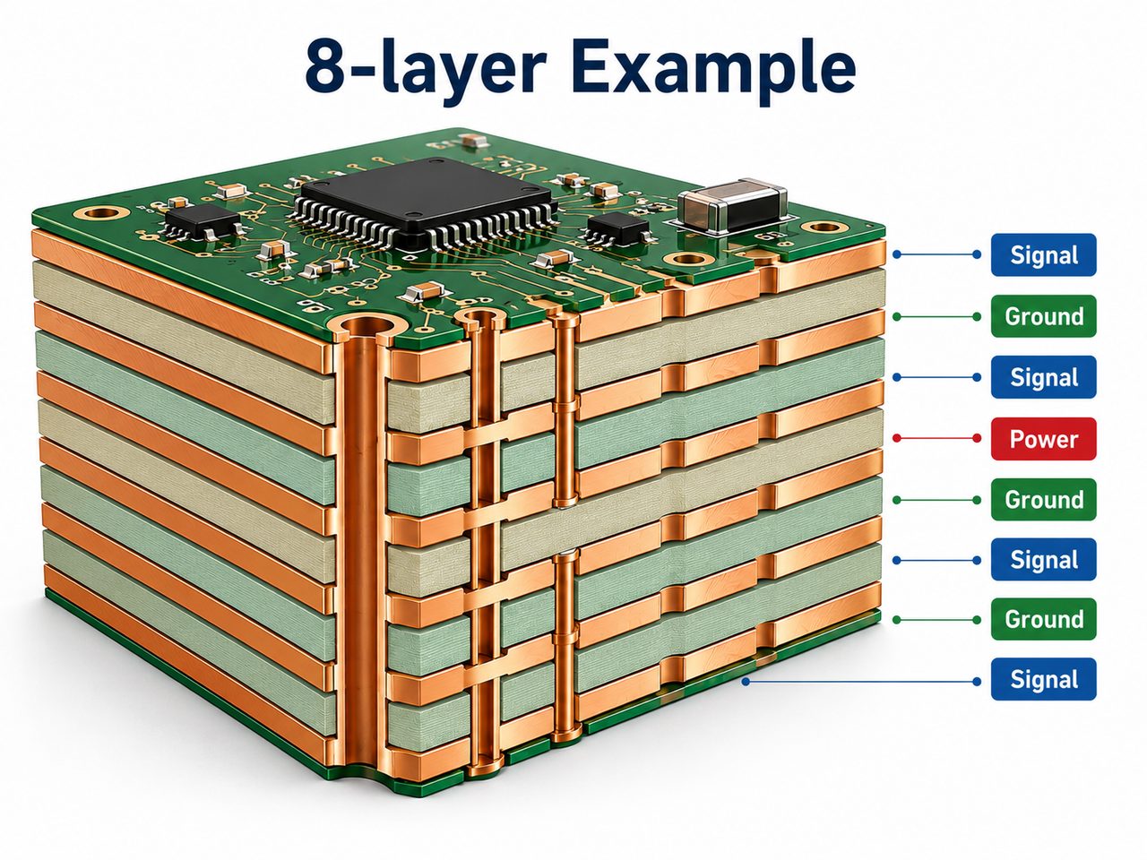
This structure provides several solid ground references and reduces reliance on a divided power layer. It can suit boards with fast clocks, DDR interfaces, sensitive analog sections, or demanding EMC targets.
An 8-layer structure becomes reasonable when 6 layers cannot support clean BGA breakout, multiple high-speed interfaces compete for routing space, or dedicated signal, ground, and power functions cannot fit comfortably.
The final arrangement still has to fit real core and prepreg options. A theoretically attractive stackup may be expensive or unstable if it depends on uncommon dielectric thicknesses.
How Do Core, Prepreg, Copper Weight, and Board Thickness Affect the Stackup?
Core, prepreg, and copper determine physical layer spacing and final board thickness. They also influence impedance, etching capability, current capacity, and mechanical stability.
Core: A core is a fully cured laminate with copper bonded to one or both sides. Its thickness is relatively stable before multilayer pressing.
Prepreg: Prepreg is partially cured resin combined with glass fabric. During lamination, the resin flows and bonds adjacent layers. Pressed thickness depends on glass style, resin content, copper distribution, and pressing conditions.
| Copper Weight | Approximate Base Thickness | Typical Use |
|---|---|---|
| 0.5 oz | 17 µm | Fine inner-layer routing |
| 1 oz | 35 µm | General signal and power circuits |
| 2 oz | 70 µm | Higher-current applications |
| 3 oz and above | 105 µm and above | Heavy-copper power boards |
Outer-layer finished copper may be thicker than the starting foil because additional copper is deposited during through-hole plating. Thicker copper supports more current but also affects minimum trace width, spacing, and impedance geometry.
Common finished thicknesses include 0.8 mm, 1.0 mm, 1.2 mm, 1.6 mm, and 2.0 mm. The selected value may be driven by connector fit, enclosure dimensions, stiffness, impedance, assembly handling, or weight.
When possible, use core and prepreg materials the fabricator regularly stocks. Unusual combinations may increase cost, lead time, and batch-to-batch variation.
How Does PCB Stackup Affect Controlled Impedance and Signal Integrity?
Controlled impedance depends on the relationship between the trace and its surrounding stackup. Trace width is only one part of the calculation.
- Finished trace width
- Finished copper thickness
- Dielectric thickness
- Material dielectric constant
- Reference-plane distance
- Differential pair spacing
- Solder mask
- Microstrip or stripline geometry
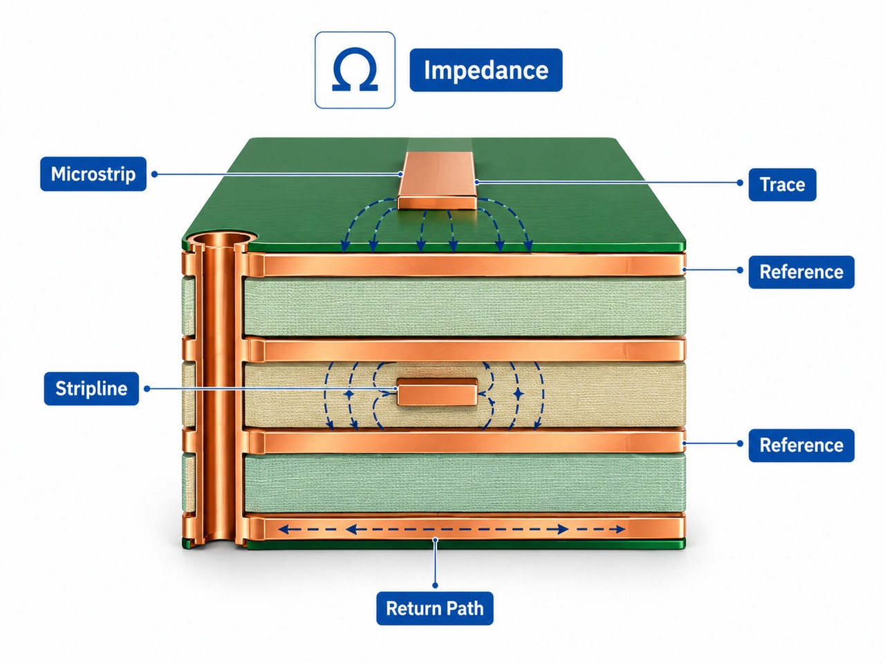
A surface microstrip is referenced to the plane beneath it. An internal stripline is placed between reference planes. These structures require different trace dimensions for the same target impedance.
Reducing the distance between a trace and its reference plane generally lowers impedance. The trace may then need to be narrowed to return to a 50-ohm target. Changes in copper thickness and material Dk also affect the result.
Reaching the calculated impedance value is not enough. The return path must remain continuous along the route. Common risks include crossing plane gaps, changing layers without nearby ground stitching vias, leaving long via stubs, and using Dk values that do not match the production laminate.
For controlled-impedance orders, the fabricator may adjust trace width or pair spacing to match actual dielectric and copper conditions. These changes should be approved before fabrication, especially around fine-pitch BGA fan-out areas.
What PCB Stackup Mistakes Cause EMI, Crosstalk, or Fabrication Problems?
Most stackup failures come from finalizing the layer arrangement before checking the real routing and production conditions.
- Routing critical signals across split planes: This interrupts the return path and increases loop area.
- Placing signal layers too far from their references: Wider field distribution makes EMI and impedance control more difficult.
- Running long parallel traces on adjacent signal layers: Broadside coupling may increase crosstalk.
- Using a divided power plane as though it were continuous: Signals may pass over several voltage regions.
- Using nominal prepreg thickness in the impedance model: Pressed thickness may differ from the catalog value.
- Creating an asymmetrical construction: Uneven copper and dielectric distribution can increase warpage.
- Ignoring finished outer copper: Plating changes trace geometry and impedance.
- Selecting uncommon material combinations: Procurement difficulty may raise cost and delay production.
- Routing before confirming the stackup: Later impedance changes can force extensive layout revisions.
- Copying an online structure without reviewing the circuit: A layer order that suits one design may restrict another.
A preliminary fabrication stackup is best requested before critical routing begins. At that stage, layer spacing, trace rules, and via structures can still be adjusted without redesigning the entire board.
What Should Be Confirmed with the PCB Manufacturer Before Finalizing the Stackup?
The manufacturer needs enough information to check lamination feasibility, impedance geometry, copper balance, and material availability.
- Required layer count and layer functions
- Finished board thickness and tolerance
- Base material, Tg, Dk, or Df requirements
- Inner and outer copper weight
- Controlled impedance targets and tolerance
- Target impedance layers and nets
- Minimum trace width and spacing
- Differential pair requirements
- Through, blind, buried, or stacked vias
- Sequential lamination requirements
- Finished hole sizes and PCB board dimensions
- Gerber, ODB++, or IPC-2581 files
- NC drill files, fabrication drawing, and preliminary stackup drawing
A note such as “50-ohm impedance required” is incomplete unless the relevant layers, trace type, and tolerance are identified.
EBest Circuit, part of Best Technology, can review a proposed construction against available laminates, copper weights, via capabilities, and impedance targets. Review our PCB manufacturing capabilities when defining material, copper, via, impedance, and inspection requirements. This is particularly useful when the prototype must use the same basic material structure planned for volume production.
FAQs About PCB Board Stackup
Q1. What is a PCB board stackup?
A PCB board stackup is the ordered arrangement of copper and dielectric layers inside a circuit board. It defines signal, ground, and power layers together with core, prepreg, copper weight, and overall thickness.
Q2. Is PCB stackup the same as PCB layer count?
No. Layer count only states the number of copper layers. Stackup also defines their functions, spacing, materials, and electrical relationships.
Q3. What is the most common 4-layer PCB stackup?
Signal / Ground / Power / Signal is one of the most common structures. It is practical for many embedded and industrial products with several power rails.
Q4. Is Signal–Ground–Power–Signal always the best 4-layer stackup?
No. It works well for many boards, but bottom-layer signals may have poor return paths if the power plane is divided. A dual-ground structure may be better when ground continuity is the main priority.
Q5. How do I choose between a 4-layer and 6-layer PCB?
Move to 6 layers when 4 layers cannot provide enough routing channels, BGA breakout space, continuous references, or power distribution. Base the decision on the layout rather than component count alone.
Q6. What is a typical 8-layer PCB stackup?
A practical example is Signal / Ground / Signal / Ground / Power / Signal / Ground / Signal. The final sequence depends on power rails, signal density, and reference-plane requirements.
Q7. Should every signal layer be next to a ground plane?
Critical high-speed layers benefit from an adjacent ground plane. Low-speed layers may reference a continuous power plane, provided the return path is not interrupted.
Q8. Does PCB board size affect the required layer count?
Yes. A smaller board may require more layers because less routing area is available. Package density, interface speed, power structure, and connector placement are often more decisive.
Q9. How does PCB stackup affect controlled impedance?
It determines dielectric thickness, copper thickness, material Dk, and reference-plane distance used in the impedance calculation.
Q10. Can a PCB manufacturer change my proposed stackup?
The manufacturer may recommend different core or prepreg combinations to match available materials and production controls. Layer functions or electrical references should not be changed without design approval.
A practical PCB board stackup balances routing density, reference-plane continuity, power distribution, impedance, material availability, and production cost. Define the layer functions early, obtain a realistic fabrication structure, and complete critical routing using confirmed dielectric and copper parameters.
For a PCB board stackup review or PCB quotation, send your board files, layer requirements, copper weight, finished thickness, and impedance targets to sales@bestpcbs.com.