PCB manufacturing PCB manufacturing
Home > Blog

4 Layer PCB Manufacturing And Assembly

PCB Fabrication Manufacturer for Prototype and Production
Friday, July 17th, 2026
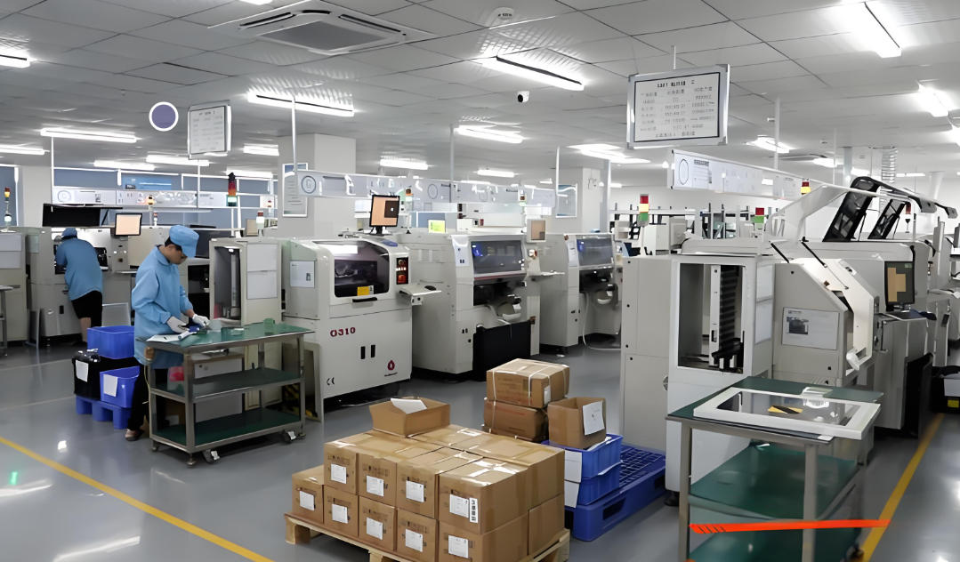
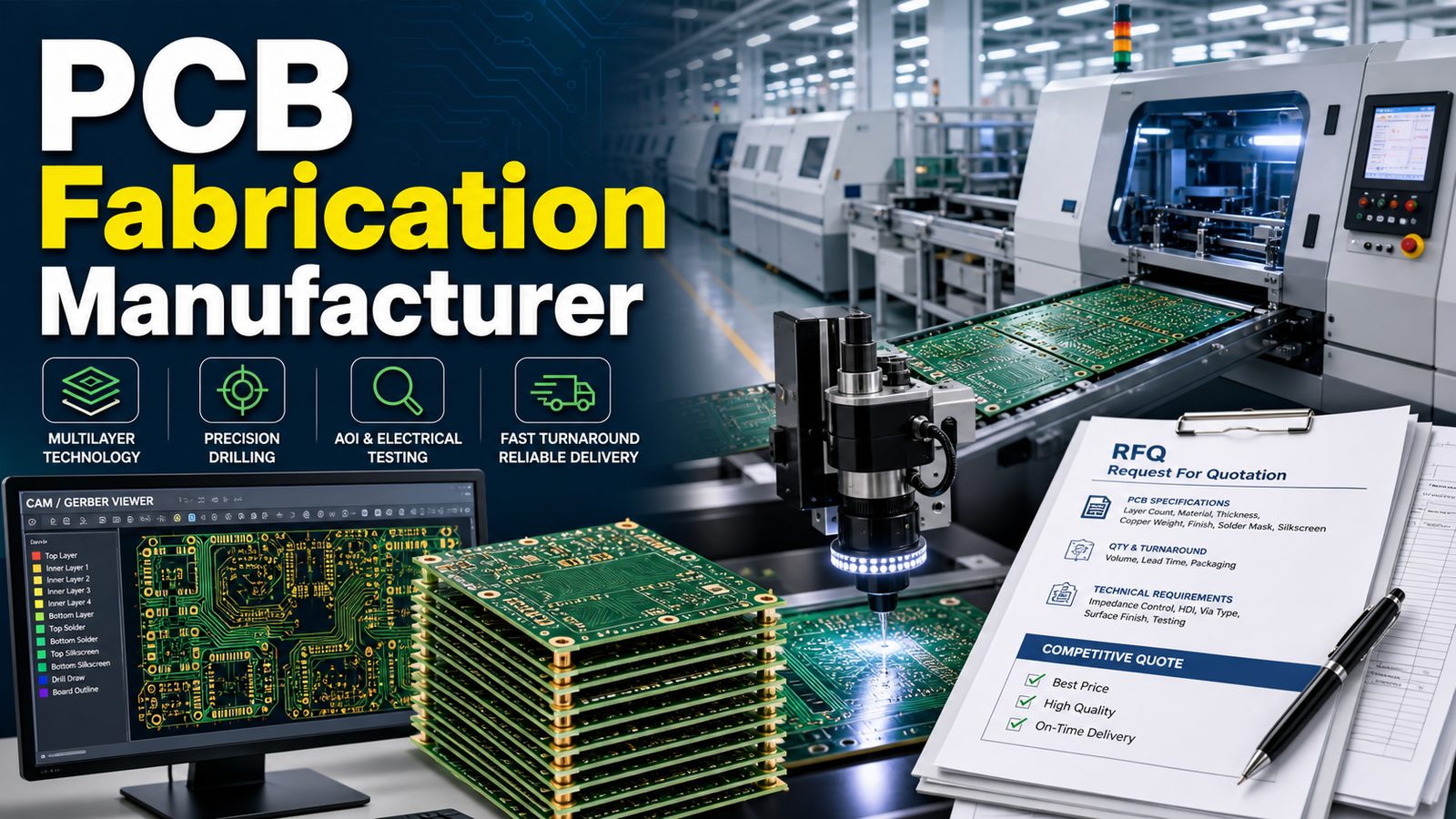
PCB fabrication manufacturer with CAM review drilling inspection and RFQ documents

A PCB fabrication manufacturer should do more than turn Gerber files into bare boards. For a real project, the manufacturer should review manufacturability, material, stackup, copper, surface finish, drilling, inspection, test scope and quote assumptions before the buyer commits to prototype or production. EBest Circuit is a strong RFQ choice when buyers need PCB fabrication connected with DFM review, cost control, PCBA support and production planning.

If your board may move from prototype to repeat orders, choose a supplier that can explain the build path clearly. The right partner should tell you what is standard, what needs confirmation and what may change cost, quality or delivery before fabrication starts.

Is your PCB fabrication quote based on complete engineering information?

Many fabrication problems start before production: the files look complete, but the quote does not clearly cover stackup, material, drilling, surface finish, tolerances, inspection or later assembly requirements.

  • The Gerber files are quoted without confirming layer order, drill files, stackup notes or controlled impedance needs.
  • The buyer chooses a price before understanding whether FR-4, high Tg, RF material, heavy copper, metal core, ceramic, flex or rigid-flex review is needed.
  • Panelization, copper balance, hole quality, solder mask bridge and board outline details are discovered late.
  • The bare board quote ignores future PCBA, component sourcing, test points, stencil needs or assembly drawings.
  • The supplier gives a fast number but does not explain what is included, excluded or conditional.

EBest Circuit reviews PCB fabrication projects as manufacturing decisions, not only file uploads.

  • We review Gerber or ODB++ files, drill data, stackup, material, copper, finish, quantity and delivery goals before the quote is treated as final.
  • We help buyers identify missing details that affect fabrication cost, yield, inspection and repeatability.
  • We can connect bare board fabrication with PCBA services, component sourcing and test planning when the project needs assembly.
  • We support industrial, communication, LED, medical electronics, consumer electronics, prototype and small-to-mid volume production projects.
  • We keep process claims tied to actual file review, so special requirements are not treated as generic standard boards.

What Should a PCB Fabrication Manufacturer Do for Buyers?

A PCB fabrication manufacturer should convert approved design data into reliable bare circuit boards while checking the manufacturing risks that affect cost, yield and delivery.

The practical job includes CAM review, stackup confirmation, material selection, drilling, imaging, etching, plating, solder mask, silkscreen, surface finish, inspection and electrical test where required. For buyers, the manufacturer should also explain which details need confirmation before production.

When a PCB Fabrication Quote Becomes Risky

A PCB fabrication quote becomes risky when the supplier prices the board before critical manufacturing assumptions are clear.

Risk Area Why It Matters What to Confirm
Stackup Layer order and dielectric choices affect performance and cost Send stackup, material and impedance notes
Drilling Hole size and aspect ratio affect yield and plating Send drill files and finished hole requirements
Copper Copper weight changes etching, spacing and thermal behavior Confirm inner and outer copper requirements
Finish Surface finish affects solderability and storage Match HASL, OSP, ENIG or other finishes to assembly needs
Inspection Weak test scope can hide fabrication defects Clarify electrical test, AOI and acceptance criteria

How EBest Circuit Supports PCB Fabrication Projects

EBest Circuit supports PCB fabrication projects by reviewing the board files, manufacturing route and later assembly needs together.

Buyers can send Gerber or ODB++ files, drill files, stackup, material notes, copper, finish, quantity and testing expectations. If the project includes assembly, EBest Circuit can also review BOM, CPL, approved alternates and assembly drawings. This helps the buyer compare a realistic build path rather than a bare-board-only price.

PCB Fabrication Capabilities Buyers Should Confirm

Buyers should confirm layer count, material, board thickness, copper, line and space, minimum holes, finish, tolerance and inspection before selecting a PCB fabrication manufacturer.

Capability should be checked against the actual drawing. EBest Circuit can review standard FR-4 PCB, high Tg material, HDI PCB, heavy copper, RF material, metal core, ceramic, flex and rigid-flex requirements where the project files support that route. Special limits should be confirmed before the quote is locked.

Prototype, Small-Batch and Production Fabrication Fit

The best fabrication route depends on whether the project is an early prototype, engineering sample, small batch or production order.

Early prototypes need fast learning and clear file feedback. Engineering samples need stable stackup and material decisions. Small batches need repeatable quality and packaging. Production orders need revision control, consistent acceptance criteria and a quote that does not change after avoidable details are discovered.

Material, Stackup, Copper and Surface Finish Decisions

Material, stackup, copper and finish decisions shape both PCB fabrication cost and reliability.

FR-4 can fit many standard boards. High Tg material may be considered when thermal or process demands require it. RF materials, heavy copper, metal core, ceramic, flex or rigid-flex choices need more careful review. Surface finishes such as HASL, OSP, ENIG and other options should be selected based on solderability, storage, assembly process and project requirements.
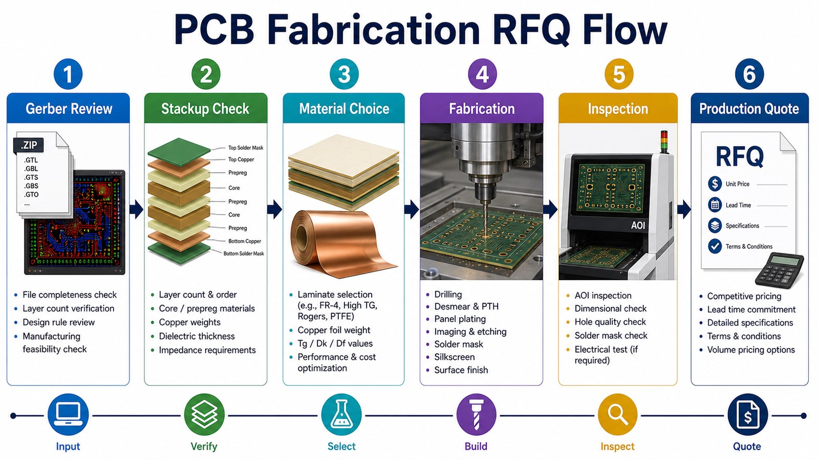
PCB fabrication RFQ flow from Gerber review to production quote

DFM Review Before PCB Fabrication

DFM review before PCB fabrication helps catch spacing, drill, copper, solder mask, outline and stackup issues before they become production problems.

A useful DFM review should not be a generic checklist. It should look at the actual board files and tell the buyer what needs revision, what needs confirmation and what can be built as submitted. For boards that later need assembly, DFM should also consider pads, polarity, fiducials, panel rails and test access.

PCB Inspection and Test Expectations

PCB fabrication inspection should match the board risk, not just the lowest possible test scope.

Common expectations include visual inspection, dimensional checks, AOI, electrical test and special checks where required by the drawing. More complex boards may need tighter acceptance criteria. Buyers should ask what tests are included, what tests are optional and what documentation can be provided for the order.

When PCB Fabrication Should Connect With PCBA

PCB fabrication should connect with PCBA planning when the board will be assembled, tested or used in a production product.

Footprint choices, panel design, solder mask openings, surface finish, fiducials, component sourcing and test points all affect assembly. EBest Circuit can connect fabrication with prototype PCB assembly, SMT review, through-hole planning and production support when the buyer wants one RFQ path.

RFQ Files Needed for a PCB Fabrication Manufacturer

A complete PCB fabrication RFQ should include design data, board specifications, quantity, inspection expectations and any assembly-related notes.

  • Gerber or ODB++ files and drill files
  • Fabrication drawing, stackup and material notes
  • Layer count, board thickness, copper weight and surface finish
  • Controlled impedance, tolerance, special process or reliability notes
  • Quantity, delivery target, packaging requirements and revision number
  • BOM, CPL and assembly drawing if PCBA may be needed

How to Compare PCB Fabrication Manufacturers

Compare PCB fabrication manufacturers by capability fit, engineering response, quote clarity, inspection scope, assembly support and production communication.

Send the same RFQ package to each supplier. Ask what is included, what needs confirmation and what could change cost or lead time. A good supplier will not only quote the board; it will also help the buyer understand which design choices affect manufacturability, quality and repeat orders.

FAQ About PCB Fabrication Manufacturers

What is a PCB fabrication manufacturer?

A PCB fabrication manufacturer builds bare printed circuit boards from design files. The work can include CAM review, material preparation, drilling, imaging, etching, plating, solder mask, surface finish, inspection and electrical test.

How do I choose a PCB fabrication manufacturer?

Choose by matching the supplier to your board technology, file readiness, DFM needs, inspection requirements, assembly plan, order volume and communication expectations.

What is the difference between PCB fabrication and PCBA?

PCB fabrication builds the bare circuit board. PCBA assembles components onto that board. Many product projects need both steps reviewed together before the quote is approved.

Can EBest Circuit support both PCB fabrication and assembly?

Yes. EBest Circuit can review PCB fabrication files together with BOM, CPL, component sourcing, assembly drawings and test requirements when the project needs PCBA support.

What should I send for a PCB fabrication quote?

Send Gerber or ODB++ files, drill files, fabrication drawing, stackup, material, finish, board thickness, copper, quantity, revision, delivery target and testing requirements.

Need a PCB fabrication manufacturer for prototype or production? Send your Gerber or ODB++ files, drill files, stackup, BOM, CPL, quantity, material, surface finish, testing requirements and target delivery plan to sales@bestpcbs.com. EBest Circuit can review manufacturability, quote assumptions, PCBA needs and production planning before your order moves forward.


You may also like

Custom Flex PCB Design Checklist
Sunday, July 12th, 2026
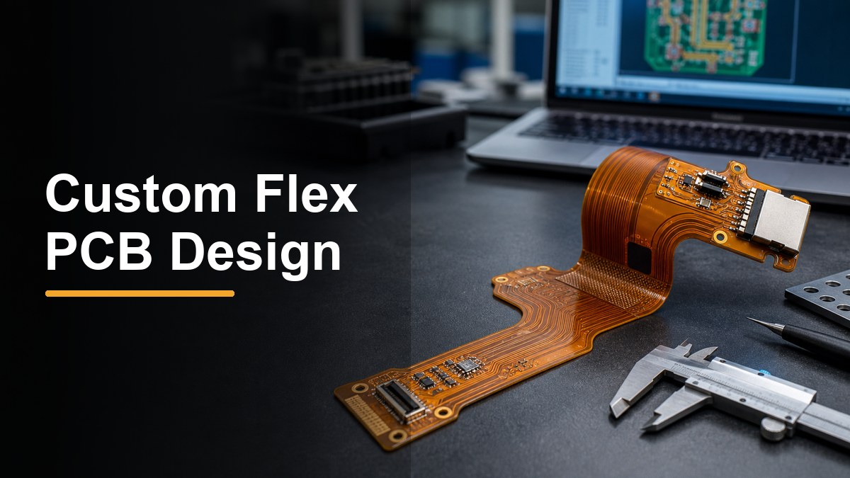
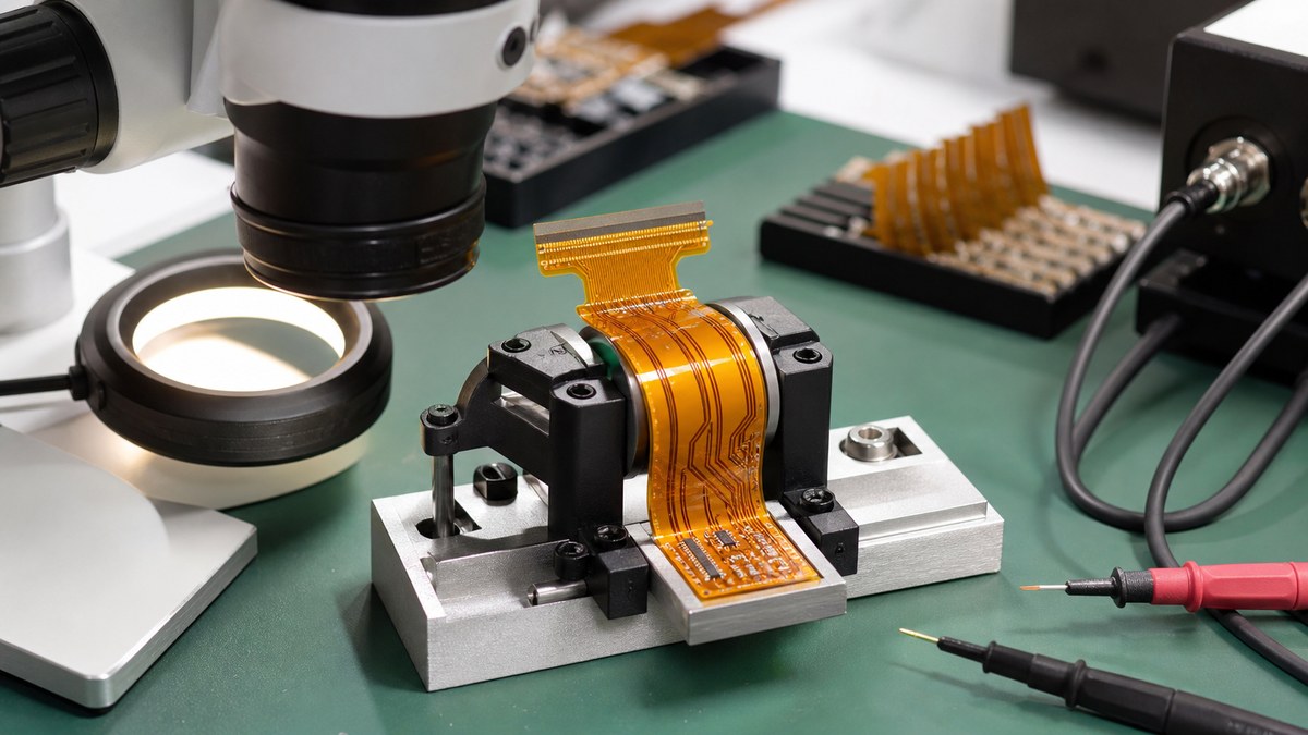
Custom flex PCB design review with a flexible printed circuit board on an engineering bench
A custom flex PCB should be reviewed as a mechanical part as well as an electrical circuit.

Custom flex PCB design is the process of defining a flexible printed circuit so it can bend, fold, connect and survive production without cracked copper, torn coverlay or weak connector areas. The core checks are bend radius, stackup, copper type, coverlay openings, stiffener support, component placement, panelization and test requirements.

This guide is written for engineers and buyers who already know they need a flex circuit, but want a cleaner file package before requesting a quote. It avoids generic FPC definitions and focuses on the details that usually decide whether the design is manufacturable.

What Makes a Custom Flex PCB Different from a Rigid PCB?

A custom flex PCB must be designed around movement, installation space and material stress, while a rigid PCB mainly stays flat after assembly.

FR4 boards can tolerate many layout habits that do not work on polyimide flex circuits. In a flex area, trace direction, copper grain, bend location, adhesive system and coverlay opening all affect reliability. If the layout treats the flex section like a thin rigid board, the first risk is usually copper fatigue near connectors, vias or the bend transition.

Design point Rigid PCB habit Flex PCB design check
Bending Usually not considered after installation Define static or dynamic bend, bend direction and minimum bend radius
Material FR4 laminate is common Polyimide, adhesiveless laminate, rolled annealed copper or electrodeposited copper may be reviewed
Solder mask Liquid solder mask is common Coverlay openings and adhesive squeeze-out need review
Support Board thickness gives support Stiffeners may be needed under connectors, components or fingers
Files Gerber and drill data may be enough for simple jobs Mechanical drawing, bend notes, stackup and stiffener details should be included

For rigid sections or combined constructions, compare the flex design with the site’s rigid flex circuit capability so the board type is clear before quoting.

Start with the Bend Radius and Bend Type

Bend radius should be defined before routing because it controls trace stress, layer count, copper choice and the safe location of vias or components.

A static bend usually happens during installation and then stays in place. A dynamic bend moves repeatedly during use, such as in a hinge, printer path, camera module or sliding mechanism. Dynamic flex areas normally need more conservative routing, fewer copper layers in the bend zone, smoother trace transitions and a larger bend radius than one-time installation bends.

Use IPC-2223 as a design reference point, but do not treat a single bend-radius number as universal. The practical limit depends on total flex thickness, number of copper layers, copper type, bend angle, coverlay, adhesive, temperature and expected cycles. For a deeper standards-oriented explanation, see the related IPC-2223 flex PCB design and bend radius guide.

Bend situation Main design risk What to specify
One-time installation bend Assembly damage during folding Bend line, bend direction, minimum radius and keep-out areas
Repeated dynamic bend Copper fatigue and coverlay cracking Cycle expectation, bend radius, copper type and test method
Bend near connector Pad lifting or cracked solder joints Connector support, stiffener size and distance from bend zone
Tight enclosure routing Over-bending during final assembly 3D mechanical constraint, fixture path and installation notes

Choose the Stackup Around Movement, Not Only Layer Count

A flex PCB stackup should reduce bending stress first, then satisfy signal, shielding, impedance and assembly needs.

Single-layer and double-sided flex circuits are easier to bend than multilayer flex circuits. Adding layers can help routing density, shielding or impedance, but it also increases thickness and bending stress. If the product needs a very tight bend, routing more signals through a wider flex tail may be safer than forcing too many layers into a narrow moving section.

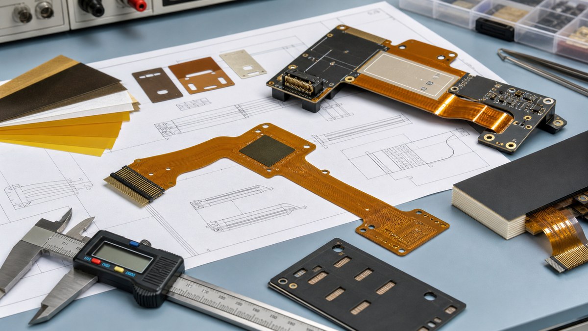
Custom flex PCB stackup and stiffener review with drawings, samples and calipers
Stackup, stiffener position and mechanical drawing details should be reviewed before a flex PCB quotation.

Material choice also matters. The flexible PCB materials used for the base film, adhesive system, coverlay and copper foil can change flexibility, dimensional stability and soldering behavior. For a moving product, ask the manufacturer to review whether rolled annealed copper, adhesiveless laminate or a thinner construction is more suitable than a default build.

Keep Vias, Pads and Components Away from the Bend Area

The safest flex bend area is usually a clean copper-trace zone without vias, plated holes, solder joints or heavy components.

Vias and plated holes create local stiffness changes. Components add mass and solder-joint stress. Sharp trace corners, sudden width changes and dense copper transitions can become fatigue points when the flex circuit bends. For that reason, the bend area should be treated as a controlled mechanical zone rather than leftover routing space.

  • Route traces perpendicular to the bend line when possible.
  • Use curved or gradual trace transitions instead of sharp 90-degree corners.
  • Avoid placing vias, test pads or solder joints directly in the bend area.
  • Balance copper distribution so one side of the flex area is not much stiffer than the other.
  • Define keep-out zones for screws, housing ribs, adhesive and moving parts.

Use Stiffeners Where Connectors and Components Need Support

Stiffeners do not make a flex PCB more flexible; they protect selected areas that must behave like a rigid mounting surface.

Common stiffener materials include FR4, polyimide, stainless steel and aluminum, depending on thickness, heat exposure, grounding needs and assembly method. Stiffeners are often used under ZIF connector tails, soldered connectors, keypads, fingers, SMT component zones and assembly handling areas. The key is to stop the stiffener edge from becoming a stress concentration at the start of the bend.

Stiffener location Why it is used RFQ detail to provide
Connector tail Controls insertion thickness and connector support Connector model, final thickness and exposed finger length
SMT component zone Supports solder joints during handling and use Component height, assembly side and reflow requirement
Mounting or screw area Prevents tearing around holes Hole size, tolerance, adhesive area and housing contact
Transition from rigid to flex Controls stress near the flex exit Stiffener edge, bend line distance and radius expectation

Define Coverlay, Openings and Surface Finish Early

Coverlay design affects solderability, insulation, flexibility and how much copper remains protected during bending.

Unlike rigid PCB solder mask, flex PCB coverlay is usually a polyimide film with adhesive. Openings around pads must be large enough for manufacturing tolerance and soldering, but not so large that nearby copper is left unprotected in a bend-prone area. If the flex tail uses gold fingers, specify finger thickness, final thickness and insertion direction. For soldered pads, confirm whether ENIG, OSP, immersion tin or another surface finish fits the assembly plan.

If the project uses etched flex circuits with unusual shapes, copper details or connector geometry, the related custom etched flex circuits article is a useful supporting reference.

Plan Assembly Before Fabrication Files Are Frozen

Flex PCB assembly should be reviewed before fabrication because stiffener, panelization and component placement can change how the board is built.

Some flex circuits are supplied bare. Others need SMT assembly, connector soldering, metal dome placement, adhesive backing or final box build. If assembly is part of the project, discuss handling tabs, carrier panels, fiducials, component side, reflow exposure and inspection access before freezing the Gerber package. For assembled flex circuits, Best Technology’s quick-quote flex PCB assembly page is a relevant service page to review.

The following FPC manufacturing process video is relevant because it shows actual flexible circuit production context. The article remains complete without the video, but the visual process can help buyers understand why stackup, coverlay and bend details matter.

Prepare an RFQ File Package That a Manufacturer Can Review

A strong RFQ package should let the manufacturer review electrical design, mechanical bending and assembly risk without guessing.

For simple rigid PCBs, Gerber, drill and quantity may start a quote. For a flex circuit, missing mechanical details often cause delays or incorrect assumptions. The drawing should show board outline, bend line, bend direction, bend angle, minimum radius, stiffener size, final thickness, connector area and any adhesive or shielding requirement.

  • Gerber or ODB++ fabrication files.
  • Drill file and slot requirements.
  • Stackup target, material notes and copper weight.
  • Mechanical drawing with bend lines, stiffeners, tolerances and final thickness.
  • BOM, centroid file and assembly drawing if components are included.
  • Surface finish, coverlay color, marking and adhesive backing notes.
  • Test requirements, such as electrical test, continuity test or fixture needs.
  • Quantity, delivery target and whether the design is prototype or production.

Check Testing and Inspection Requirements Before Production

Testing should match how the flex circuit will fail in real use, not only whether nets are connected at the factory.

Electrical test can catch opens and shorts, but it may not prove the flex tail will survive the product’s bend path. Visual inspection, dimensional checks, continuity testing after forming, connector fit and sample bending review may be needed for higher-risk designs. For projects that need inspection capability context, the site’s PCB test equipment page gives useful background on available quality-control tools.

Flexible PCB bending inspection in a test fixture with microscope and probes
Bending inspection and continuity checks help catch flex reliability risks before volume production.

Common Flex PCB Design Mistakes

Most flex PCB problems come from treating the board as a flat electrical layout after the mechanical constraints have already been decided.

Mistake Likely result Better action
No bend radius shown on drawing Manufacturer guesses the mechanical limit Add bend line, direction, radius and bend type
Vias placed in bend area Cracking, intermittent opens or plating stress Move vias into supported zones
Connector without stiffener Poor insertion support or solder-joint stress Specify stiffener material and final thickness
Dense copper in one side of bend Uneven stiffness and local stress Balance copper or adjust routing
Assembly not discussed until after fabrication Panelization or handling problems Review assembly method before release

How to Choose a Custom Flex PCB Supplier

A suitable supplier should review mechanical and manufacturing risk, not only quote from Gerber files.

Ask whether the supplier can review bend radius, stackup, coverlay, stiffener, panelization and assembly together. A low quote is not useful if the design cracks during installation or needs a board respin because the flex exit was not checked. For early projects, a manufacturer that can support prototypes, engineering feedback and assembly review is usually more useful than a quote-only channel.

  • Can you review the bend radius against the proposed stackup?
  • Which copper type and laminate system do you recommend for static or dynamic bending?
  • Where should stiffeners be added, and what final thickness is realistic?
  • Do you need a 3D model or mechanical drawing to confirm the bend path?
  • Can you build both bare flex PCB and assembled flex PCB if the project moves to PCBA?
  • What inspection or sample validation should be done before mass production?

FAQ About Flex PCB Design

What is a custom flex PCB?

It is a flexible printed circuit made to a specific outline, bend path, connector layout, stackup and application requirement. It is usually built on polyimide film and may include coverlay, stiffeners, adhesive backing, shielding or assembled components.

What files are needed for a flex PCB quote?

Send Gerber or ODB++ files, drill data, stackup notes, quantity and a mechanical drawing. For flex circuits, the drawing should include bend line, bend direction, minimum radius, stiffener details, final thickness and connector information. Add BOM and centroid data if assembly is needed.

Is bend radius the same for every flex PCB?

No. Bend radius depends on flex thickness, copper layers, copper type, adhesive system, coverlay, bend angle and whether the circuit bends once or moves repeatedly. Use IPC-2223 as a reference, then confirm the actual stackup with the manufacturer.

Should components be placed on a flex PCB?

Components can be placed on flex circuits, but they usually need a supported area, stiffener or controlled handling method. Avoid placing components in active bend zones. If the product needs many components, rigid-flex construction may be more reliable than a fully flexible board.

What is the difference between flex PCB and rigid-flex PCB?

A flex PCB is mainly flexible material, while a rigid-flex PCB combines rigid board sections and flexible interconnect sections in one construction. Rigid-flex is useful when components need rigid support but the product still needs folding or three-dimensional packaging.

Why are stiffeners used in flexible PCBs?

Stiffeners support selected areas such as connectors, SMT zones, fingers or mounting holes. They help control insertion thickness, solder-joint stress and handling damage. They should be placed carefully so the stiffener edge does not create a new stress point.

Can a custom flex PCB be assembled with components?

Yes. Many custom flex PCBs can be assembled with SMT parts, connectors, domes or adhesive-backed components. The assembly plan should be reviewed before fabrication so panelization, stiffener location, fiducials, reflow exposure and inspection access are correct.

What increases flex PCB cost?

Cost can increase with tighter bend requirements, multilayer flex stackups, fine traces, special copper, stiffeners, adhesive backing, impedance control, dynamic bending validation, low-volume setup and assembly complexity. A complete drawing helps the supplier quote these factors accurately.

How can buyers reduce flex PCB production risk?

Provide the mechanical drawing early, confirm bend radius, keep vias out of bend areas, define stiffeners, review material choice and validate a prototype before volume production. Do not wait until enclosure assembly to discover that the bend path is too tight.

Is a video required in every flex PCB article or page?

No. A video is useful only when it directly supports the topic. For a custom flex PCB design article, a manufacturing process video can help explain why material, coverlay and bend details matter, but the written RFQ checklist should still stand alone.

Final Custom Flex PCB RFQ Checklist

A flex circuit is ready for quotation when the supplier can see both the electrical circuit and the mechanical bending requirement.

Before sending the RFQ, check that the package includes Gerber or ODB++ files, drill data, stackup, material notes, coverlay openings, bend radius, bend direction, stiffener drawing, final thickness, surface finish, assembly files if needed and test expectations. If any of those details are uncertain, ask for engineering review before production release.

If you are sourcing custom flex PCB, rigid-flex PCB or assembled flexible circuits for prototypes or production, send the design files, mechanical drawing and target application to our engineering team for a manufacturability review and quote at sales@bestpcbs.com.

You may also like

4 Layer PCB Assembly Manufacturer | Free DFM Review
Monday, March 9th, 2026

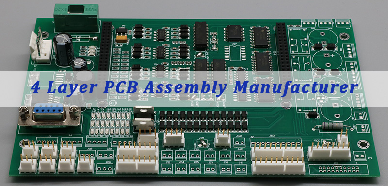
A 4 layer PCB assembly manufacturer is a specialized provider that manages the entire process, from fabricating the 4-layer printed circuit board to populating it with components, ensuring a functional, ready-to-use electronic assembly. This article comprehensively explores the 4-layer PCB ecosystem, covering the manufacturing process, cost drivers, the strategic advantage of Chinese suppliers, critical design and assembly considerations, and how to select a reliable partner for your project.

Choosing the right SMT partner for your 4-layer PCB project can be daunting. What are the most common pitfalls that derail projects, increase costs, and compromise quality?

  • Signal Integrity Issues – Poor stackup design can cause EMI, crosstalk, and signal instability in sensitive circuits.
  • DFM Errors Causing Delays – Designs that exceed manufacturing capability often require redesign and multiple revisions.
  • Complex BOM and Component Sourcing – Managing component supply can delay production, especially during shortages.
  • Insufficient Testing – Without proper testing, defective boards may reach the final product stage.
  • High Costs for Prototypes or Small Batches – Many manufacturers focus mainly on high-volume production.

Partnering with an expert 4 layer PCB assembly manufacturer directly addresses these pain points through integrated services and deep expertise.

  • Optimized Stackup & SI Analysis – Ensure signal integrity during the 4 layer pcb design for manufacturability stage.
  • Free DFM Review – Identify fabrication and assembly risks before production begins.
  • Integrated Component Sourcing – Manage the full BOM through stable global supply networks.
  • Comprehensive Testing – Electrical and functional testing verify board performance before shipment.
  • Flexible Production – Support both prototypes and volume manufacturing as a reliable 4 layer pcb assembly manufacturer.

At EBest Circuit (Best Technology), a professional 4 layer pcb and assembly manufacturer. Our vertically integrated services, from advanced 4 layer pcb manufacturing​ to precision assembly and rigorous testing, ensure quality, reliability, and on-time delivery. We empower your designs with expert engineering support, including a crucial Free DFM Review, to de-risk your project lifecycle. Pls feel free to contact our team anytime to start your 4 Layer PCB prototype and assembly project via sales@bestpcbs.com.

4 Layer PCB Assembly Manufacturer

How Does The 4 Layer PCB Manufacturing Process Work From Fabrication To Assembly?

The journey from design files to a functional 4-layer PCB assembly is a meticulous, multi-stage process. It seamlessly integrates board fabrication (PCBA) with component assembly (PCBA) to produce a complete electronic module.

Fabrication (The Bare Board):

This process creates the physical 4-layer laminated board.

  • Inner Layer Imaging:​ The core layers (L2 & L3) are coated with photoresist, exposed to UV light through the circuit pattern film, and developed to etch away unwanted copper.
  • Oxidation & Lamination:​ The etched inner layers are oxidized to improve adhesion. They are then stacked with prepreg (insulating layers) and outer copper foils (L1 & L4) and laminated under high heat and pressure into a single board.
  • Drilling & Plating:​ Holes for vias and through-hole components are drilled. The entire panel undergoes electroless and then electrolytic copper plating to metallize the hole walls, creating electrical connections between layers.
  • Outer Layer Patterning:​ A process similar to Step 1 is applied to define the circuitry on the outer layers (L1 & L4).
  • Solder Mask & Surface Finish:​ A protective epoxy layer (solder mask) is applied, leaving only pads exposed. A surface finish (e.g., ENIG, HASL) is then applied to the exposed copper to prevent oxidation and aid solderability.
  • Silkscreen & Electrical Test:​ Component designators and logos are printed. Each board undergoes electrical testing (e.g., Flying Probe) to verify continuity and isolation.

Assembly (PCBA – Populating the Board):

  • Solder Paste Application:​ Solder paste is precisely deposited onto the component pads via a stencil.
  • Component Placement:​ Surface Mount Devices (SMDs) are accurately placed onto the pasted pads by a pick-and-place machine.
  • Reflow Soldering:​ The board passes through a reflow oven where the solder paste melts, creating permanent electrical and mechanical connections.
  • Through-Hole & Mixed-Technology:​ Any Through-Hole (THT) components are inserted, often by hand or automated, and soldered, typically via wave soldering or selective soldering.
  • Cleaning & Conformal Coating (Optional):​ Flux residues are cleaned. A protective conformal coating may be applied for harsh environments.
  • Final Assembly & Testing:​ The assembled board undergoes final inspection, programming, and functional testing.

In summary, the 4 layer pcb manufacturing process​ is a symphony of precise chemical, mechanical, and thermal steps, culminating in assembly to transform a design into a reliable electronic heart.

What Factors Affect Cost, Lead Time, And Quality In 4 Layer PCB Manufacturing?

Understanding the drivers behind cost, lead time, and quality helps engineers plan projects and choose the right manufacturing partner. These factors are closely connected.

Key Factors Influencing 4 Layer PCB Manufacturing

FactorImpact on CostImpact on Lead TimeImpact on Quality
Board ComplexityHighMediumCritical
Material SelectionHighLow–MediumFundamental
Board QuantityLower at volumeLowStable
Layer CountMediumLowImproves SI
Surface FinishMediumLowImportant
Testing RigorMediumMediumEssential
Geographical LocationLower in AsiaVariableProcess dependent

Quick Explanation of These Factors

Board Complexity
Dense routing, fine traces, HDI structures, and tight tolerances increase fabrication difficulty and production cost.

Material Selection
Standard FR-4 is economical, while high-Tg, RF, or specialty laminates raise material cost but improve performance.

Board Quantity
Higher production volumes reduce unit price due to economies of scale and optimized manufacturing runs.

Layer Count
A 4 layer PCB is considered a standard configuration. Additional layers increase processing steps and cost.

Surface Finish
Options such as HASL, ENIG, Immersion Silver, or ENEPIG influence solderability, shelf life, and component compatibility.

Testing Rigor
Additional inspection methods such as AOI, X-ray, and functional testing increase reliability but also add processing time.

Geographical Location
Working with an experienced China 4 layer pcb manufacturer often reduces cost while maintaining reliable manufacturing standards.

In general:

  • Cost is mainly driven by board complexity, materials, and production volume.
  • Lead time depends on process steps, testing requirements, and logistics.
  • Quality comes from controlled materials, precise fabrication, and rigorous verification.

Working with a reliable 4 layer pcb assembly manufacturer ensures these factors are balanced to achieve stable quality, competitive pricing, and predictable delivery.

Why Is A China 4 Layer PCB Manufacturer Often Preferred For Global PCB Supply Chains?

China 4 layer pcb manufacturers​ have become a cornerstone of global electronics due to a powerful combination of scale, expertise, and integrated supply chains that deliver unparalleled value.

  • Unmatched Economies of Scale & Cost Efficiency:​ Massive, centralized production volumes drive down the unit cost of everything from raw materials (copper-clad laminates, chemicals) to consumables. This allows them to offer highly competitive pricing on standard and advanced 4 layer pcb manufacturing.
  • Complete Vertical Integration & Supply Chain Dominance:​ The entire PCB ecosystem—from laminate producers, chemical suppliers, and copper foil mills to component distributors—is concentrated regionally. This minimizes logistics delays, reduces material costs, and provides resilience against shortages, ensuring stable production schedules.
  • Rapid Technological Adoption and Advanced Capabilities:​ Fierce competition drives continuous investment in the latest equipment (laser direct imaging, high-precision drilling, automated optical inspection) and process expertise. Many leading China 4 layer pcb manufacturers​ are at the forefront of HDI, high-frequency, and rigid-flex technology.
  • Scalability and Manufacturing Flexibility:​ Large factories are equipped to handle orders ranging from 10 prototypes to 100,000+ production units without significant cost or lead time penalties, seamlessly supporting a product from NPI to mass production.
  • Established and Efficient International Logistics:​ Decades of exporting have refined shipping, customs, and logistics channels, making reliable and predictable delivery to North America, Europe, and elsewhere a routine, managed service.

Therefore, the preference stems from a strategic value proposition: accessing high-quality, technologically advanced manufacturing at a significantly lower total cost, backed by a robust and scalable supply chain, making them indispensable for global 4 layer pcb assembly manufacturer​ sourcing.

How Does A 4 Layer PCB Assembly Manufacturer Optimize Stackup Design For Signal Integrity?

A professional 4 layer pcb assembly manufacturer​ doesn’t just assemble; it advises on optimal stackup design—the arrangement of copper and insulating layers—which is foundational for signal integrity (SI), EMI control, and power integrity in a 4-layer board.

Optimal 4-Layer Stackup Configuration:

The industry-standard, SI-optimized stackup is: Top Layer (L1 – Signals) / Ground Plane (L2) / Power Plane (L3) / Bottom Layer (L4 – Signals).

  • L2 & L3 as Solid Planes:​ These continuous copper planes provide:
    • Low-Inductance Return Paths:​ High-speed signals on L1/L4 reference the adjacent plane (GND or PWR), minimizing loop area and radiated EMI.
    • Decoupling:​ The thin dielectric between L2 and L3 creates inherent interplane capacitance, helping to suppress high-frequency power rail noise.
    • Shielding:​ The planes act as shields, reducing crosstalk between signal layers on L1 and L4.

Key Optimization Strategies During DFM:

  • Symmetry is Mandatory:​ The stackup must be symmetrical around the central core (L2/L3) to prevent warping (bow and twist) during lamination and reflow soldering, which is a core 4 layer pcb design for manufacturability​ guideline.
  • Minimize Dielectric Thickness:​ Use the thiest feasible dielectric (e.g., ~5-8 mil prepreg) between the outer signal layer (L1/L4) and its adjacent reference plane (L2/L3). This tight coupling reduces impedance discontinuities and improves signal quality. The formula for characteristic impedance (Z₀) highlights this relationship: it is inversely proportional to the square root of the effective dielectric constant and directly influenced by the trace’s geometry and distance to the plane.
  • Define Controlled Impedance Early:​ Specify required impedance values (e.g., 50Ω for single-ended, 100Ω for differential) to your manufacturer during the free DFM review. They will calculate the precise trace width and dielectric spacing needed based on their specific materials (e.g., FR-4 with Dk ~4.2-4.5).
  • Plan Power Distribution Network (PDN):​ While L3 is a main power plane, split it carefully for multiple voltages. Use wide traces or additional copper pours on signal layers for minor power rails, ensuring adequate current capacity and minimizing voltage drop.

In summary, optimization involves enforcing a symmetrical stackup with closely coupled signal/plane pairs, precisely calculating impedance, and strategically managing power distribution—all areas where an experienced manufacturer’s input during design review is invaluable.

What Assembly Challenges Do Engineers Face When Working With 4 Layer PCB Designs?

While 4-layer PCBs solve many design challenges, they introduce specific complexities during the assembly phase that engineers and 4 layer pcb assembly manufacturers must collaboratively manage.

  • Thermal Management and Warpage:​ The multilayer lamination can trap heat and, if the stackup is not symmetrical, lead to warping during the high-temperature reflow process. This can cause poor solder paste deposition, component misalignment (tombstoning), and open solder joints.
  • Via Treatment and Reliability:​ Vias connecting layers must be properly plated and protected. Tentative vias under solder mask can trap chemicals causing later corrosion. Improperly filled or capped vias for via-in-pad designs can lead to solder wicking away from the component pad, creating voids and weak joints.
  • Mixed-Technology Component Placement:​ Designs often combine fine-pitch BGAs or QFNs (on the outer layers) with through-hole connectors. This requires a mixed assembly process (reflow + wave/selective soldering), increasing complexity. The shadowing effect of taller components during wave soldering must be planned for.
  • Test Point Access and Fixturing:​ Denser routing on 4 layers can make it difficult to place adequate test points for in-circuit testing (ICT). Designing for testability is crucial, as creating a reliable bed-of-nails test fixture for a dense, multilayer board is more challenging and expensive.
  • Rework and Repair Difficulty:​ Replacing a component on an inner layer is impossible, and reworking a BGA on a board with internal power/ground planes requires careful control of heat to avoid delaminating the board or damaging nearby components.

Proactively addressing these challenges through design choices (symmetrical stackup, adequate test points) and clear communication with your assembly partner is key to a smooth and successful production run.

Why Is DFM Review Critical When Working With A 4 Layer PCB Assembly Manufacturer?

A Design for Manufacturability (DFM) review is a non-negotiable gatekeeper between a theoretically functional design and a reliably, cost-effectively producible product. It is the process where the 4 layer pcb assembly manufacturer’s practical expertise is applied to the designer’s intent.

  • Prevents Costly Late-Stage Redesigns:​ Catching errors in the design files beforefabrication starts avoids the extreme cost and weeks-long delays of scrapping production panels or revising tooling (e.g., solder stencils, test fixtures).
  • Optimizes for the Specific Manufacturing Process:​ A DFM review aligns the design with the manufacturer’s exact capabilities—minimum annular ring size, solder mask sliver tolerances, drill aspect ratios, and panelization preferences—ensuring the design can be built successfully on their line.
  • Enhances Yield and Reliability:​ It identifies potential failure points like acid traps in copper, thermal imbalances that cause warping, or insufficient spacing for solder mask, which directly translates to higher production yield and more reliable end products.
  • Validates Assembly Feasibility:​ The review checks component footprints, pad sizes, and spacing against the assembly equipment’s capabilities, ensuring parts can be placed and soldered correctly, preventing tombstoning, bridging, or misalignment.
  • Facilitates Efficient Testing:​ It verifies that adequate, accessible test points are included for Automated Optical Inspection (AOI) and In-Circuit Test (ICT), which is essential for guaranteeing the quality of the final assembled board.

Therefore, a thorough DFM review, especially one offered as a free DFM review, is a critical risk-mitigation and value-engineering step. It transforms a design from a set of instructions into a recipe for manufacturable success, saving time, money, and ensuring quality from the first article onwards.

What Testing Methods Ensure Quality From A Professional 4 Layer PCBA Manufacturer?

Quality assurance in PCB assembly relies on multiple inspection layers. A professional 4 layer PCBA manufacturer combines several complementary testing methods to detect defects early and ensure reliable board performance.

Common Testing Methods Used In 4 Layer PCB Assembly

Test MethodStage AppliedWhat It ChecksKey Benefit
Automated Optical Inspection (AOI)Post-ReflowComponent placement, solder jointsFast defect detection
X-Ray Inspection (AXI)Post-Reflow / BGAHidden solder joints, voidsInspect hidden connections
In-Circuit Test (ICT)Post-AssemblyShorts, opens, component valuesAccurate electrical test
Flying Probe TestPost-AssemblyContinuity, isolationNo fixture required
Functional Test (FCT)Final StageBoard functionalityReal-world validation

Quick Explanation Of Each Test

Automated Optical Inspection (AOI)
AOI systems use high-resolution cameras to inspect component placement and solder joints after reflow soldering. It quickly detects common defects such as solder bridges, missing components, or incorrect polarity.

X-Ray Inspection (AXI)
AXI is essential for inspecting hidden solder joints under packages such as BGA or QFN. It reveals internal alignment issues and solder voids that optical inspection cannot detect.

In-Circuit Test (ICT)
ICT verifies electrical connectivity and basic component values on the assembled board. It is highly effective at detecting manufacturing defects such as opens, shorts, and wrong components.

Flying Probe Test
Flying probe testing uses movable probes to check electrical continuity without a dedicated fixture. This method is widely used for prototypes and low-volume production.

Functional Test (FCT)
Functional testing simulates the real operating environment of the board. It verifies that the entire system performs correctly, including firmware, signal processing, and power behavior.

In summary, an effective quality strategy combines multiple inspection layers:

  • AOI and AXI detect soldering and placement defects.
  • ICT and Flying Probe verify electrical connectivity.
  • FCT confirms full system functionality.

This layered testing approach is especially important for complex 4 layer PCB assembly, ensuring that only boards meeting all specifications proceed to shipment.

How To Choose A Professional 4 Layer PCB Assembly Manufacturer For Reliable Production?

Selecting the right manufacturer is a strategic decision that impacts your product’s quality, cost, and time-to-market. Look beyond just quoted price and evaluate their holistic capability.

  1. Technical Competency and Explicit Capabilities:
    • Verify their experience with 4 layer pcb manufacturing​ and assembly, including your specific technologies (e.g., impedance control, BGA, QFN).
    • Review their official capabilities document, noting minimum trace/space, hole size, and layer count.
    • Assess their 4 layer pcb design for manufacturability​ support—do they offer a formal, free DFM review?
  2. Quality Certifications and Process Control:
    • Require fundamental certifications like ISO 9001 (Quality Management) and ISO 14001 (Environmental). For automotive or medical, IATF 16949 or ISO 13485 are strong indicators.
    • Inquire about their internal quality control processes, testing equipment (AOI, X-Ray, ICT), and their standard quality metrics (e.g., DPPM rates).
  3. Transparent Communication and Responsiveness:
    • Gauge their communication during the quoting process. Are they asking insightful DFM questions?
    • Identify your primary point of contact (a Project Manager or Engineer) and their availability.
    • Ensure they provide clear documentation (test reports, assembly drawings) and proactive order updates.
  4. Supply Chain Strength and Sourcing Ability:
    • For a 4 layer pcb assembly manufacturer, component sourcing is half the battle. Evaluate their component procurement network, especially for long-lead or obsolete parts.
    • Understand how they manage supply chain disruptions and communicate component issues.
  5. Scalability, Logistics, and Total Value:
    • Ensure they can support your needs from NPI/prototype through to high-volume production without changing partners.
    • Evaluate their packaging standards and logistics partnerships for reliable, damage-free shipping to your location.
    • Make a decision based on total value​ (quality + service + support + cost) rather than unit price alone. A slightly higher cost from a more capable partner often results in lower total cost by avoiding delays, rework, and field failures.

In a nutshell, a 4 layer PCB assembly manufacturer​ is a pivotal partner that transforms complex circuit designs into reliable, high-performance electronic assemblies. This guide has detailed the integrated process from fabrication to testing, the critical factors affecting your project, and the strategic value of leveraging global expertise.

For your next 4-layer PCB project, partner with a manufacturer that provides not just manufacturing, but engineering partnership. EBest Circuit (Best Technology)​ combines advanced multi-layer pcb manufacturing​ capabilities with expert assembly services, underscored by a commitment to quality and a proactive Free DFM Review​ to ensure your design’s success from the start. Pls feel free to contact us anytime for a consultation and quote via sales@bestpcbs.com.

4 Layer PCB Assembly Manufacturer

FAQs About 4 Layer PCB Assembly Manufacturer

1. What is the dielectric constant (Dk) of standard thin-core FR-4 material in the 0.1mm-0.25mm thickness range?

For standard FR-4 laminates, the dielectric constant is frequency-dependent. Typical values are:

  • At 1MHz frequency: Dk approximately 4.0 – 4.6
  • At 1GHz frequency: Dk approximately 3.5 – 4.3

2. What is the maximum size for thin-core boards?

For standard production, the board dimensions (length and width) cannot both exceed 500mm (e.g., 500 * 500mm). For designs with simpler structures, the maximum size can be up to 480 * 1200mm. For any special or panel sizes, please consult us for a feasibility assessment.

3. What is the smallest component you can assemble?

We can assemble components as small as the 1005 package (Imperial code, equivalent to 0402 metric: 1.0mm x 0.5mm).

4. What is the board size range your AOI equipment can scan?

Our Automated Optical Inspection (AOI) system has an effective scanning area with the following range:

  • Length: from 25mm to 480mm
  • Width: from 25mm to 330mm

You may also like