To make a PCB, you first turn a circuit idea into a schematic, convert the schematic into a PCB layout, export manufacturing files, fabricate the bare board, assemble components, inspect solder joints, and test the finished assembly. For a reliable result, the process should be treated as an engineering workflow, not only as a drawing or etching task.
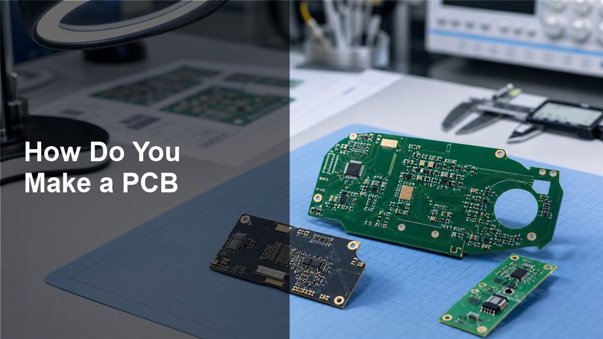
This guide explains how a PCB is made from a practical design and manufacturing perspective. It covers the steps a designer, engineer, buyer, or sourcing team should understand before sending files to a PCB manufacturer or PCBA supplier.
Start With the Circuit Requirement
A PCB project should start with the circuit function, operating environment, component needs, and production goal.
Before drawing the board, define what the circuit must do, how much current it carries, what voltage levels are involved, which signals are sensitive, and whether the board must fit inside a mechanical enclosure. Also decide whether the PCB is only for a prototype, a small engineering build, or a product that may later move into mass production.
This early definition affects material choice, board size, layer count, trace width, connector position, test points, assembly method, and cost. A simple sensor board may only need two layers, while a compact control board with high-speed signals may need more layers, controlled impedance, tighter spacing, and stronger documentation.
Create the Schematic
The schematic is the electrical map that shows components, nets, power rails, connectors, and circuit relationships.
In the schematic stage, select real components, check datasheets, assign symbols, define power input, add protection where needed, and confirm that every signal has a clear source and destination. Use meaningful net names for power, ground, communication buses, and important signals so the layout and review process are easier.
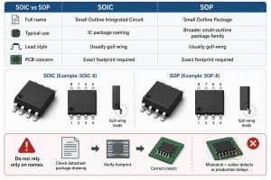
Good schematic work also includes checking component availability, package options, voltage ratings, current ratings, and thermal limits. If a part has several package choices, confirm which footprint will be used before the PCB layout begins.
Convert the Schematic Into a PCB Layout
The PCB layout turns the electrical schematic into physical copper traces, pads, vias, planes, and board outlines.
During layout, place connectors and mechanical parts first, then position ICs, power components, decoupling capacitors, crystals, sensors, and critical signal paths. Keep related components close together, route power and ground carefully, and leave enough space for assembly, inspection, and rework.
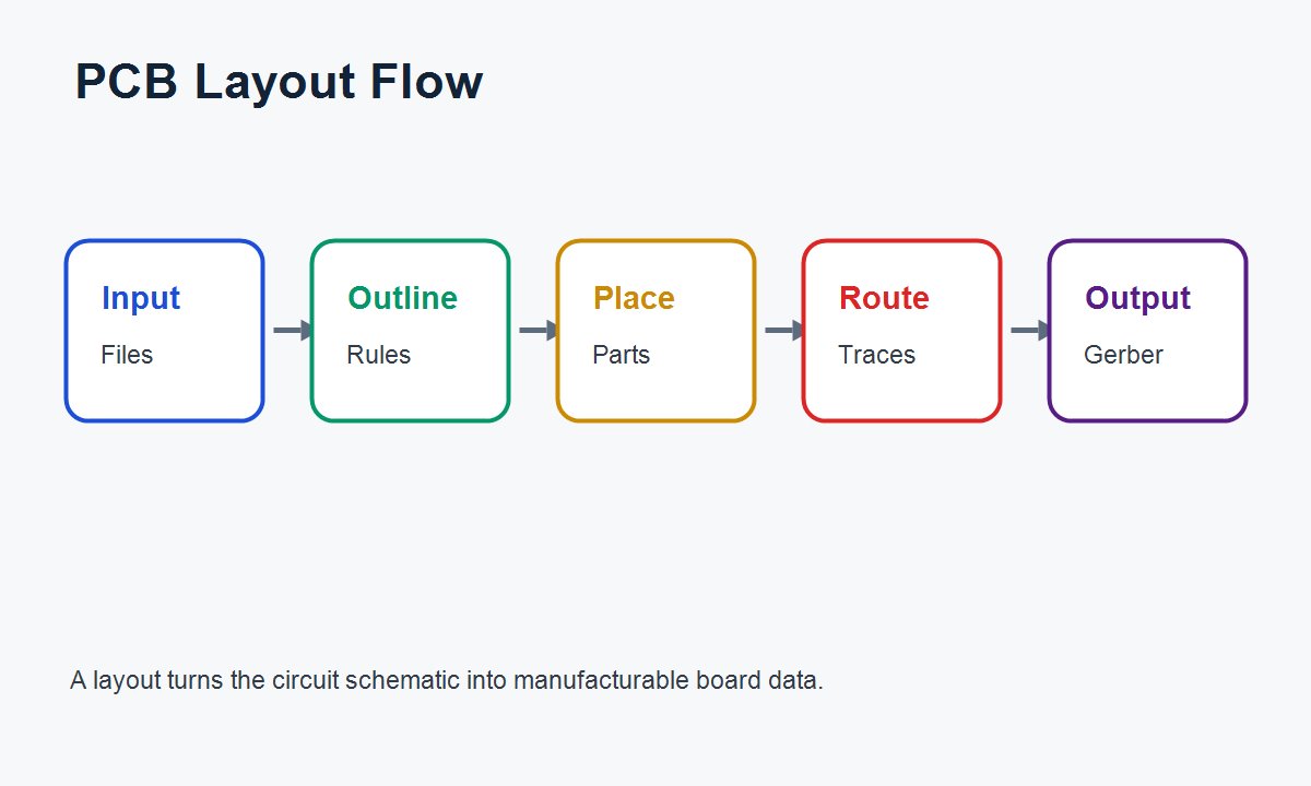
Design rules should match the PCB manufacturer capability. Check minimum trace width, minimum spacing, drill size, annular ring, solder mask clearance, copper thickness, via type, and board thickness before finalizing the layout. Using rules that are too aggressive can increase cost or create manufacturing risk.
Prepare PCB Manufacturing Files
Manufacturing files tell the factory exactly how to build the bare PCB.
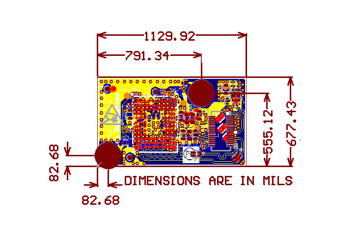
The most common file package includes Gerber files, drill files, board outline, stackup notes, copper thickness, solder mask color, silkscreen requirements, surface finish, impedance notes if needed, and fabrication drawings for controlled dimensions or tolerances. For assembly, add a BOM, pick-and-place file, assembly drawing, polarity notes, and special handling requirements.
| File or Note | What It Controls | Why It Matters |
| Gerber files | Copper, solder mask, silkscreen, paste, and board outline layers | Defines the physical board pattern used for fabrication |
| Drill files | Plated and non-plated holes | Controls vias, mounting holes, and through-hole component holes |
| Stackup notes | Layer order, dielectric thickness, copper weight, impedance needs | Important for multilayer boards and signal performance |
| BOM | Component part numbers, quantities, values, and packages | Required for sourcing and PCBA assembly |
| Pick-and-place file | Component coordinates and rotation | Helps automated assembly place parts accurately |
Run DFM Checks Before Fabrication
DFM checks help catch layout and file problems before the board enters production.
Useful checks include missing board outline, mismatched drill files, insufficient solder mask clearance, copper too close to the edge, unreadable silkscreen, tiny annular rings, incorrect footprints, polarity ambiguity, and spacing that does not match the factory capability. These issues are easier to fix before ordering boards than after fabrication.
For assembled boards, also check part availability, alternate parts, component orientation, fiducials, panelization, stencil openings, thermal pads, and test access. Small layout changes can improve assembly yield and reduce manual rework.
Fabricate the Bare PCB
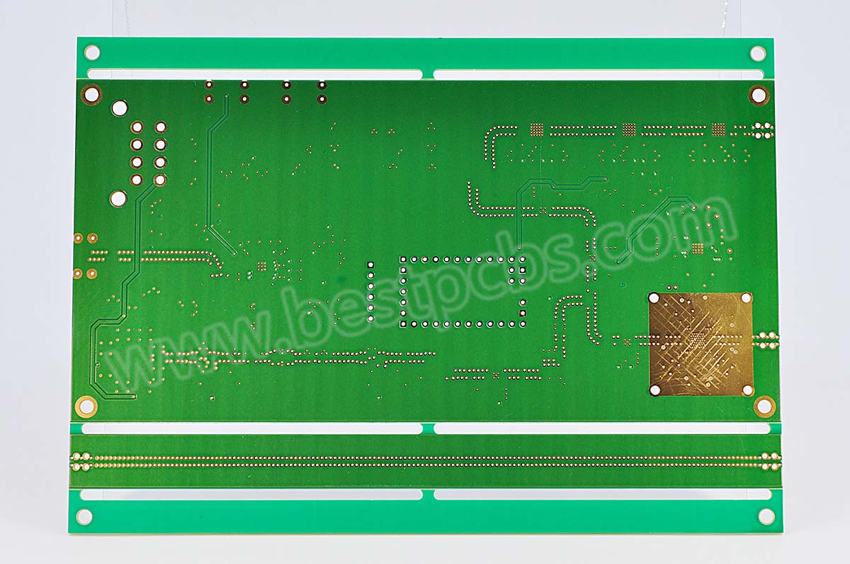
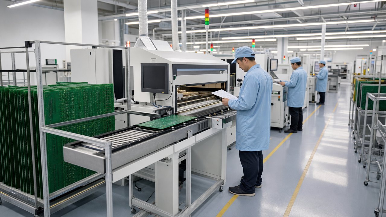
PCB fabrication builds the physical board by processing laminate, copper layers, drilled holes, plating, solder mask, silkscreen, and surface finish.
A simplified fabrication flow includes material preparation, inner layer imaging for multilayer boards, lamination, drilling, copper plating, outer layer imaging, etching, solder mask application, silkscreen printing, surface finish, profiling, electrical test, and final inspection. Exact steps depend on layer count, material, copper thickness, via structure, and surface finish.
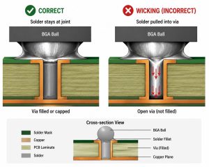
Common surface finishes include HASL, lead-free HASL, ENIG, immersion silver, immersion tin, OSP, and others. The right choice depends on component pitch, shelf life, solderability, cost, and application requirements. Fine-pitch parts, BGAs, or high-reliability assemblies often need more careful surface finish selection.
Assemble the Components
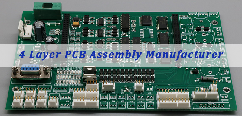
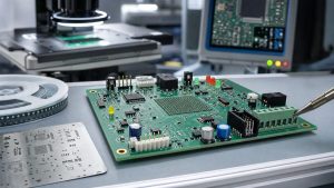
PCB assembly places and solders components onto the fabricated board.
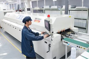
For SMT assembly, solder paste is usually printed through a stencil, components are placed by machine, and the board passes through controlled reflow. Through-hole parts may be hand soldered, wave soldered, or selective soldered depending on volume, component type, and board design.
Assembly quality depends on footprint accuracy, stencil design, solder paste volume, component orientation, reflow profile, thermal balance, and inspection. Dense boards, BGAs, QFNs, fine-pitch ICs, and mixed technology boards need stronger process control than simple prototype boards.
Inspect and Test the PCB
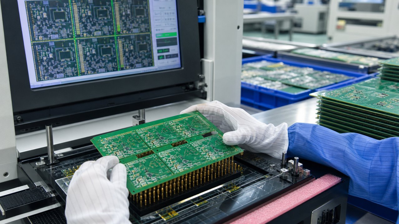
Inspection and testing confirm that the board was built correctly before it is shipped or used in a product.
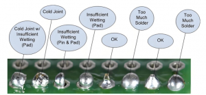
Bare boards may go through electrical testing, visual inspection, dimensional checks, and solder mask inspection. Assembled boards may use AOI, X-ray for hidden solder joints, in-circuit test, functional test, continuity checks, and first article inspection depending on the application.
Do not rely only on whether the board powers on. A board can appear functional but still have weak solder joints, marginal clearances, missing components, incorrect substitutions, or process risks that affect later reliability.
Prototype Before Mass Production
A prototype helps confirm the design, files, components, assembly process, and test plan before larger production.
Use the prototype stage to validate the schematic, layout, mechanical fit, connector position, thermal behavior, signal quality, firmware access, and production documentation. Record any manual rework because it may reveal footprint errors, missing test points, incorrect polarity markings, or assembly access problems.
If the prototype passes, update the design files and production notes before scaling. The most useful prototype is not only a working board, but a learning step that improves repeat production.
Common Mistakes When Making a PCB
Many PCB problems come from weak file preparation, unclear requirements, or layout choices that ignore manufacturing and assembly limits.
| Mistake | Possible Result | Prevention |
| Using unverified footprints | Parts do not fit or solder correctly | Compare footprints with datasheets and actual packages |
| No clear board outline | Factory must ask for clarification or may route incorrectly | Include a defined mechanical layer and fabrication drawing |
| Ignoring manufacturer design rules | Higher cost, delays, or fabrication risk | Set trace, spacing, drill, annular ring, and mask rules early |
| Missing polarity markings | Assembly errors or damaged components | Make diode, LED, capacitor, IC, and connector orientation clear |
| No test points | Difficult debugging and production testing | Add accessible points for power, ground, programming, and critical signals |
What Should You Send to a PCB Manufacturer?
A manufacturer needs clear files, specifications, and production requirements to quote and build the board correctly.
For bare PCB fabrication, send Gerber files, drill files, board dimensions, layer count, material preference, copper thickness, board thickness, solder mask color, silkscreen color, surface finish, quantity, and special requirements. For PCBA, also include the BOM, pick-and-place file, assembly drawing, component sourcing notes, firmware or programming needs, and test requirements.
If you are unsure whether the files are complete, ask for an engineering review before production. A file check can catch missing drill data, unclear stackup, unsuitable footprints, and assembly concerns before they become real cost or schedule problems.
FAQ About How Do You Make a PCB
How do you make a PCB step by step?
You make a PCB by defining the circuit, drawing a schematic, creating the PCB layout, exporting Gerber and drill files, running DFM checks, fabricating the bare board, assembling components, inspecting solder joints, and testing the finished board.
Can I make a PCB at home?
You can make simple single-sided boards at home using hobby methods, but home PCB making is limited in accuracy, plating, solder mask, vias, and repeatability. For reliable prototypes or production boards, professional fabrication is usually safer.
What files are needed to make a PCB?
For bare PCB fabrication, the usual files are Gerber files, drill files, board outline, and fabrication notes. For assembly, also provide a BOM, pick-and-place file, assembly drawing, polarity notes, and test requirements.
How long does it take to make a PCB?
Lead time depends on layer count, material, surface finish, quantity, complexity, assembly needs, and supplier capacity. Simple prototypes can be faster than multilayer, impedance-controlled, high-density, or assembled boards. Confirm timing with the manufacturer before ordering.
What is the difference between PCB fabrication and PCB assembly?
PCB fabrication makes the bare printed circuit board with copper, holes, solder mask, silkscreen, and surface finish. PCB assembly places and solders components onto that bare board, then inspects and tests the assembled product.
Do I need a schematic before making a PCB?
Yes, a schematic is strongly recommended because it defines the circuit and net relationships. You can sometimes copy a simple board layout directly, but a schematic makes checking, debugging, and future revisions much safer.
What software is used to make a PCB?
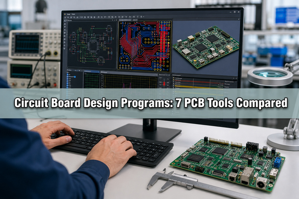
Common PCB design tools include KiCad, Altium Designer, Eagle, Fusion 360 electronics tools, OrCAD, and other EDA platforms. The right tool depends on design complexity, team workflow, file requirements, and budget.
Why is DFM important when making a PCB?
DFM checks confirm that the layout matches manufacturing and assembly limits. They help prevent delays, extra cost, soldering problems, missing files, weak clearances, and design choices that a factory cannot build reliably.
Can a PCB manufacturer help check my files?
Many PCB manufacturers can review Gerber files, drill data, stackup notes, BOMs, and assembly files before production. The review does not replace design responsibility, but it can catch practical fabrication and assembly issues.
What is the most common reason a first PCB fails?
Common reasons include wrong footprints, reversed polarized components, missing pull-up or pull-down resistors, poor power layout, unclear connectors, inadequate test points, and design rules that do not match the manufacturer capability.
Final Thoughts
Making a PCB is a connected process: circuit definition, schematic, layout, manufacturing files, fabrication, assembly, inspection, and testing all affect the final result. A clean layout is not enough if the files are incomplete, the footprints are wrong, or the assembly requirements are unclear.
If you are preparing a PCB or PCBA project, BestPCBs can support prototype development, PCB fabrication, PCB assembly, OEM/ODM manufacturing, and engineering file review. Send your Gerber files, BOM, drawings, quantity, and special requirements to sales@bestpcbs.com for technical support and a quote.