Through hole vs surface mount are the two main methods for attaching electronic components to a printed circuit board, and each serves different design and manufacturing needs.
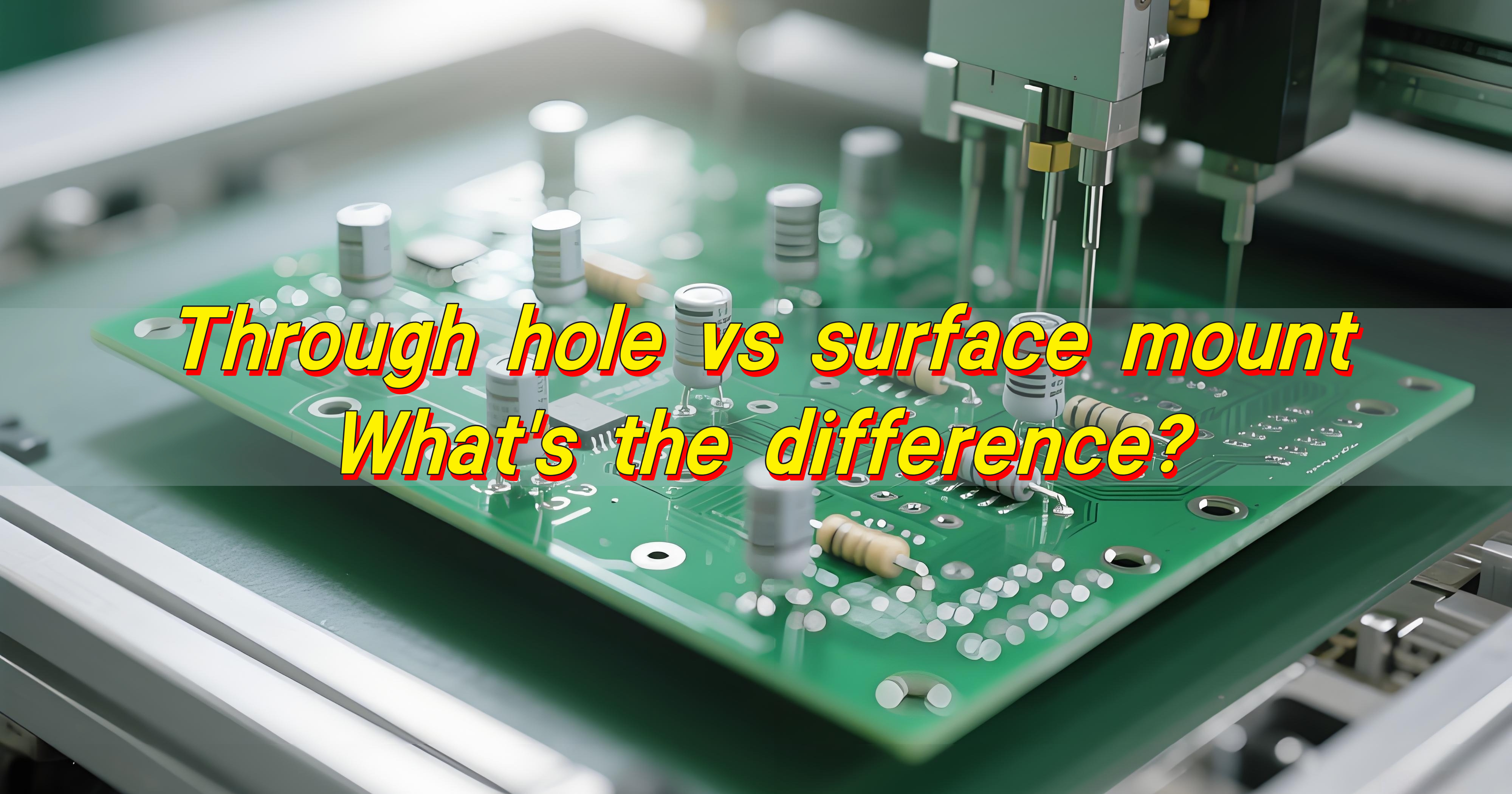
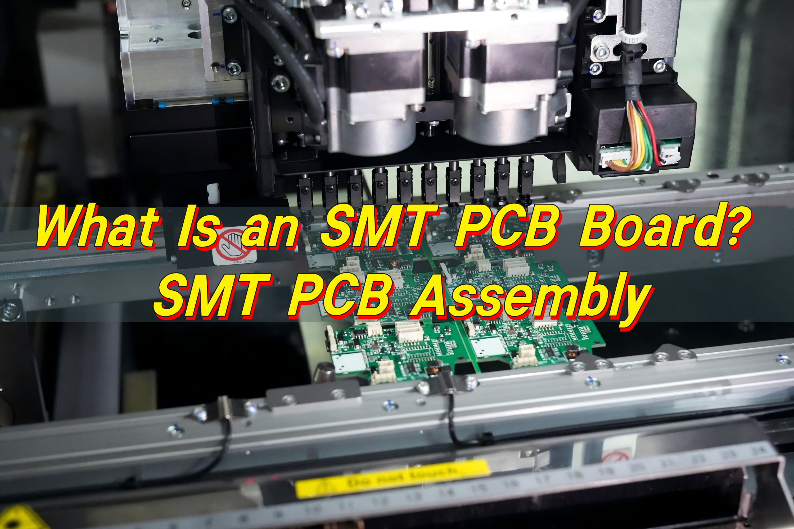
What Is the Difference Between SMT and THT?
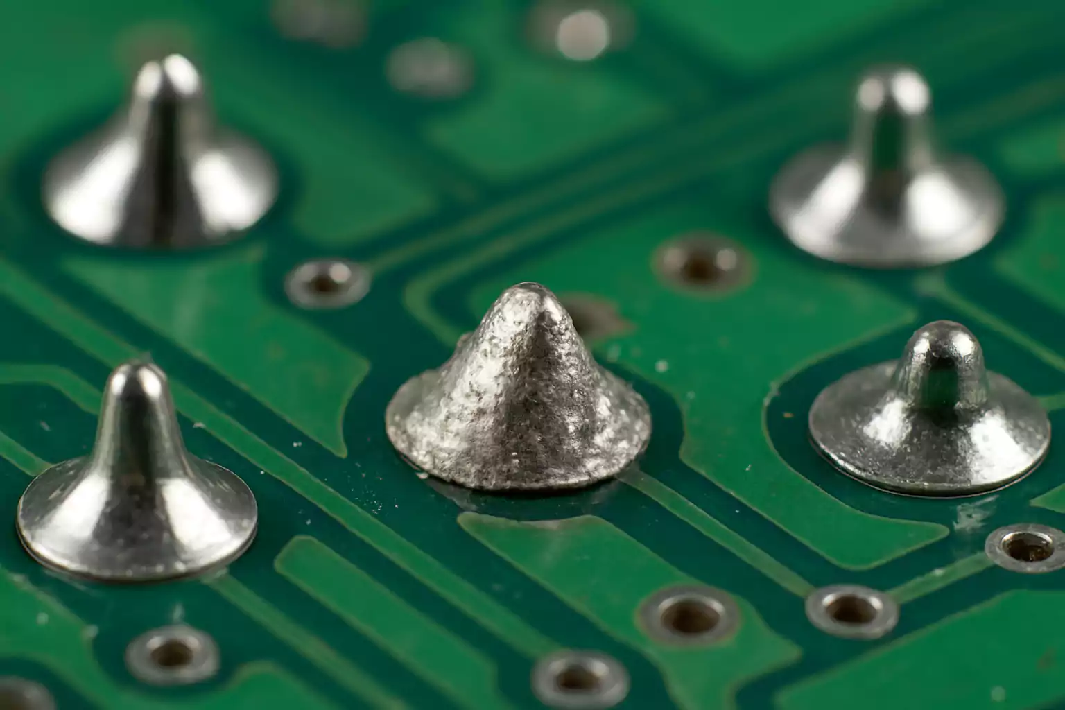
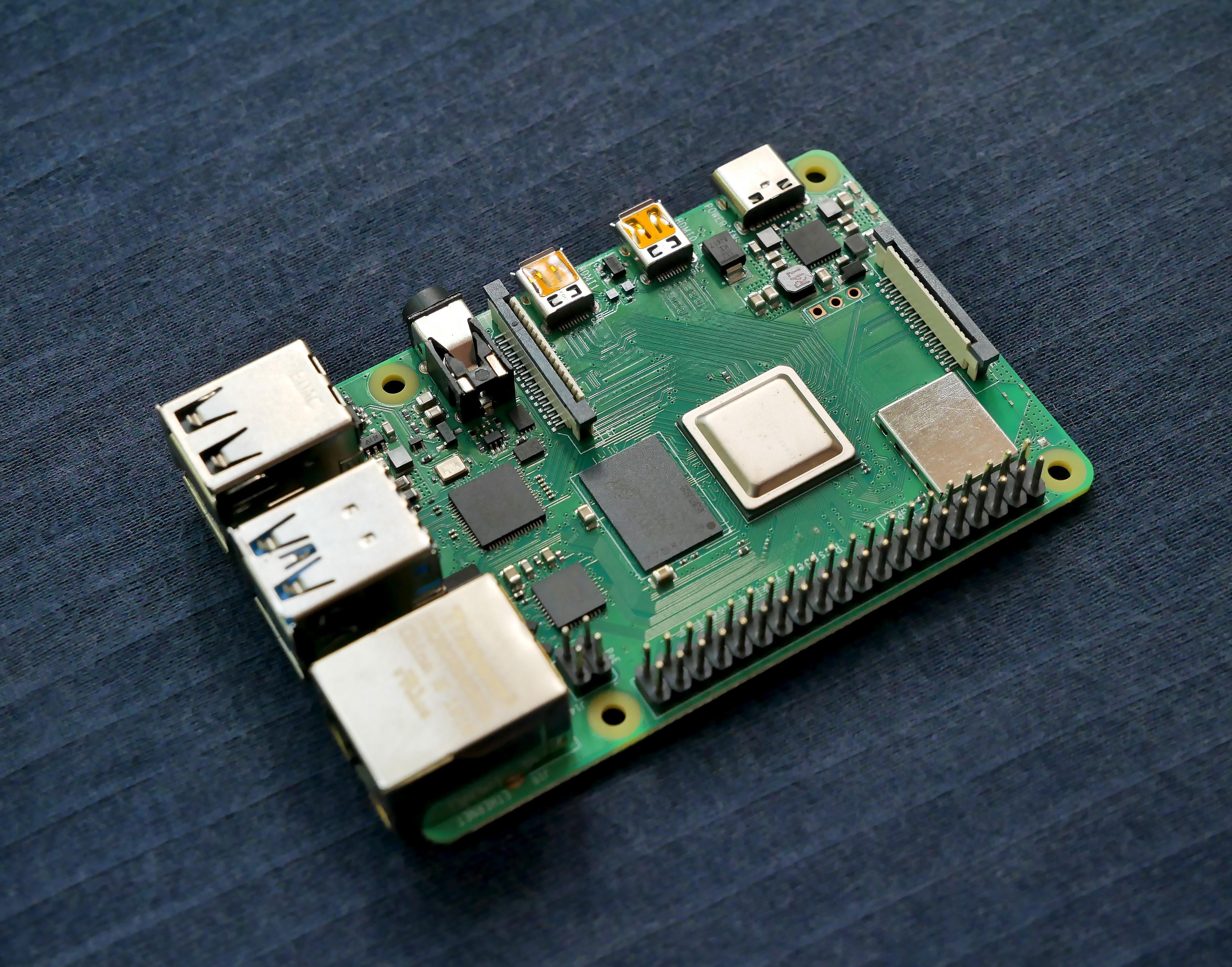
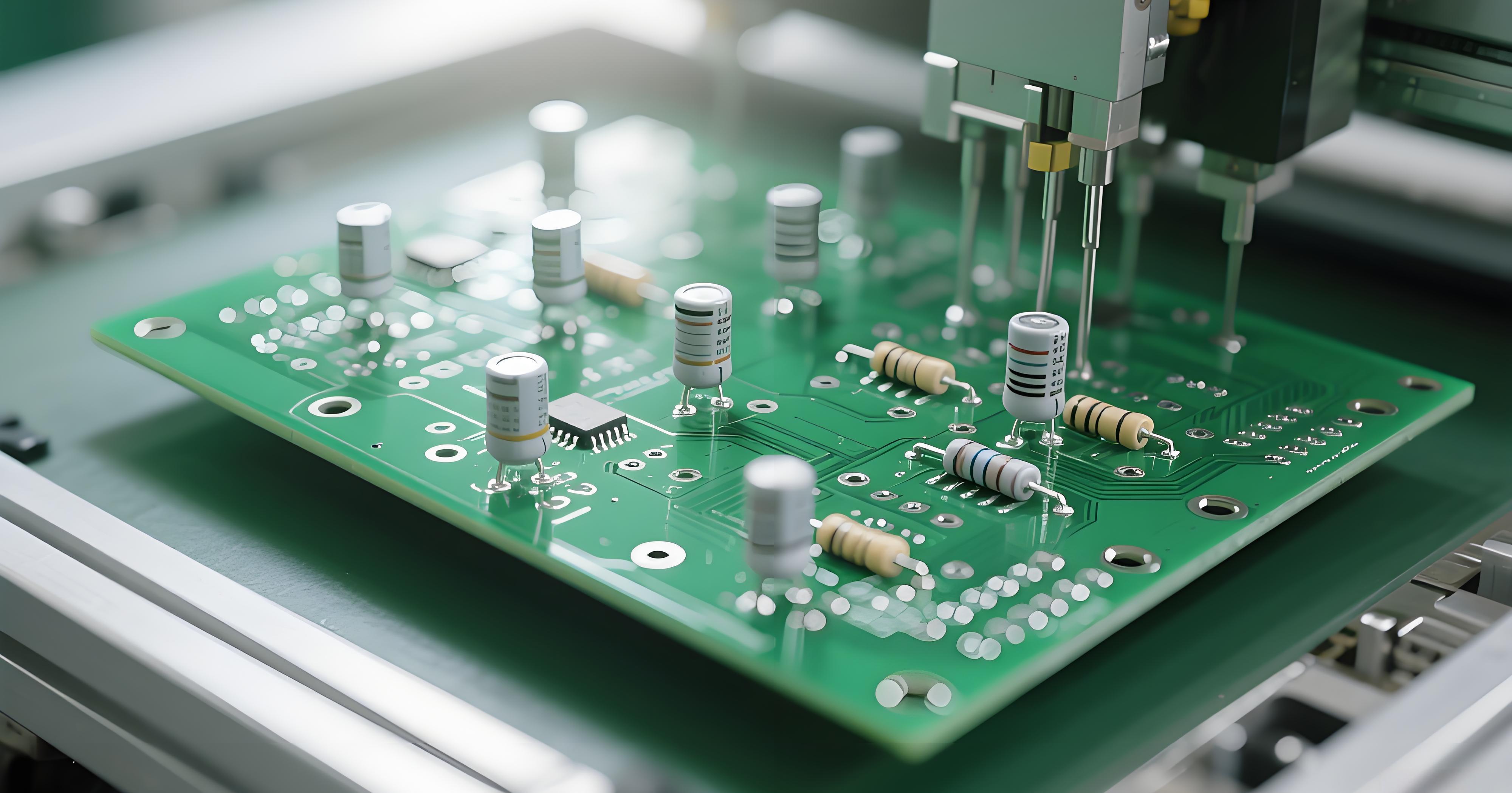
Through hole technology, often called THT or through hole mount, uses component leads that pass through drilled holes in the PCB. These leads are inserted, soldered on the opposite side, and mechanically anchored by the plated hole wall. This method relies heavily on through hole drilling, copper plating, and solder fillets that form on both sides of the board.
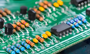
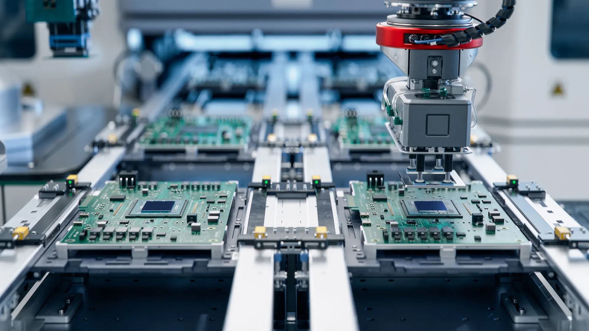
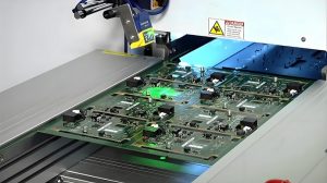
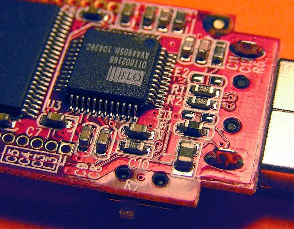
Surface mount technology, or SMT, works very differently. Components are placed directly onto pads on the PCB surface. No lead passes through the board. Instead, solder paste holds the part in place during reflow. This approach supports compact layouts, fine-pitch parts, and high-speed automated placement.
From a manufacturing view, the difference between PCB through hole vs surface mount affects many steps:
- Through hole requires drilling, desmear, and hole plating
- SMT focuses on stencil printing, placement accuracy, and reflow profiling
- THT boards often need wave soldering or selective soldering
- SMT boards rely on reflow soldering and AOI inspection
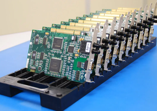
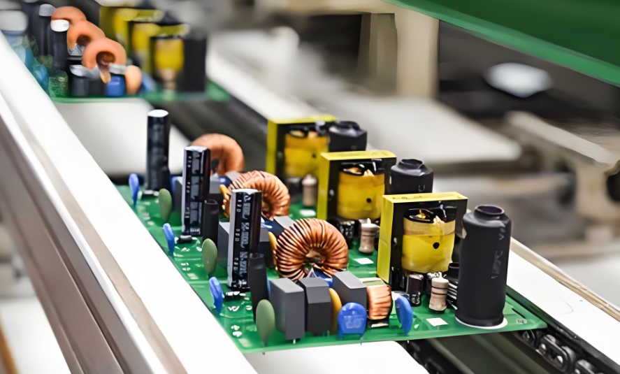
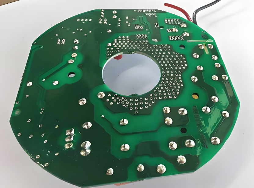
At EBest Circuit (Best Technology), mixed-technology boards are common. Many designs use surface mount components for logic and control, while keeping through hole components for connectors, transformers, or power devices.
What Are the Disadvantages of SMT?
Surface mount technology delivers speed and density, but it is not without limitations.
- One challenge is mechanical strength. Surface mount parts rely entirely on solder joints attached to surface pads. Under heavy vibration or mechanical stress, these joints need proper pad design and solder volume to remain stable.
- Thermal handling can also be more demanding. Small surface mount packages dissipate heat through pads and copper planes. Poor thermal design may cause overheating if copper balance or via placement is incorrect.
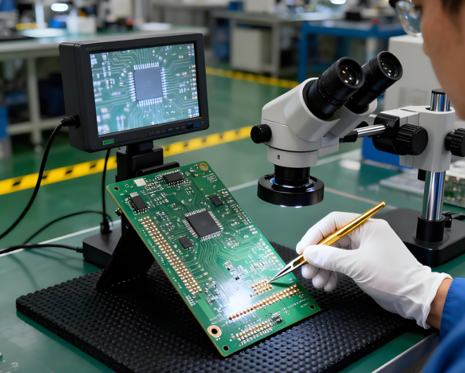
- Another consideration is inspection and rework. Fine-pitch SMT components require magnification, X-ray inspection, and skilled rework processes.
Common SMT challenges include:
- Sensitivity to solder paste quality
- Tight process windows in reflow profiles
- Higher dependency on accurate PCB fabrication
- Increased difficulty in manual rework for very small packages
Experienced manufacturers, including EBest Circuit (Best Technology), mitigate these issues through controlled stencil design, profile tuning, and process validation.
What Are the Disadvantages of Through-Hole Soldering?
When reviewing surface mount vs through hole soldering, through hole soldering presents a different set of trade-offs.
- The most visible limitation is space. Through hole components occupy both sides of the PCB and require clearance around each drilled hole. This reduces routing density and limits miniaturization.
- Manufacturing time is another factor. Through hole soldering often involves manual insertion or slower automated processes. Wave soldering is efficient for large volumes, but setup and fixturing take time.
- Cost is also influenced by drilling. Each plated hole adds fabrication steps, tool wear, and inspection effort. For dense designs, through hole drilling increases PCB cost compared to pure SMT layouts.
Despite these points, through hole technology remains valuable. Its disadvantages are mostly related to scale and size, not reliability. For power and structural roles, its benefits often outweigh its limits.
Is Surface Mount Better Than Through-Hole?
Surface mount excels in high-density electronics. It supports smaller boards, faster assembly, and lower per-unit cost at volume. Consumer electronics, IoT devices, and compact control modules rely heavily on SMT for this reason.
Through hole shines where strength and current handling matter. Large electrolytic capacitors, power inductors, relays, and connectors benefit from the mechanical anchor of plated holes.
What Is the Main Advantage of SMT Over Through-Hole Technology?
The main advantage of SMT over through hole technology is efficiency. This efficiency appears in several practical ways.
- First, component density increases. Surface mount packages are smaller and do not require holes, allowing more components per square inch.
- Second, automation improves consistency. SMT lines place thousands of parts per hour with repeatable accuracy.
- Third, electrical performance benefits. Shorter leads reduce parasitic inductance and resistance, which helps high-speed and high-frequency designs.
Key advantages include:
- Reduced board size
- Faster assembly cycles
- Improved signal integrity
- Lower material usage at volume
What Is THT Used For?
Through hole technology remains essential in many applications. Its use is deliberate
THT is commonly used for components that experience physical stress or carry high current. Power supplies, industrial controllers, and automotive modules often include through hole parts for durability.
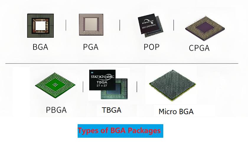
Typical through hole components types include connectors, transformers, large capacitors, and mechanical switches. These parts benefit from the mechanical bond formed by the plated hole and solder fillet.
THT is also common in prototypes and low-volume builds. Manual insertion allows flexibility during early design stages. Educational boards and test fixtures often rely on through hole mount parts for ease of handling.
At EBest Circuit (Best Technology), THT is frequently integrated into hybrid PCBA projects. Selective soldering and controlled wave soldering ensure reliable joints without compromising SMT sections.
What Is the Golden Rule of Soldering?
The golden rule of soldering is simple: heat the joint, not the solder.
This principle applies to both surface mount soldering vs through hole processes. Proper solder joints form when the pad and lead reach the correct temperature, allowing solder to flow naturally.
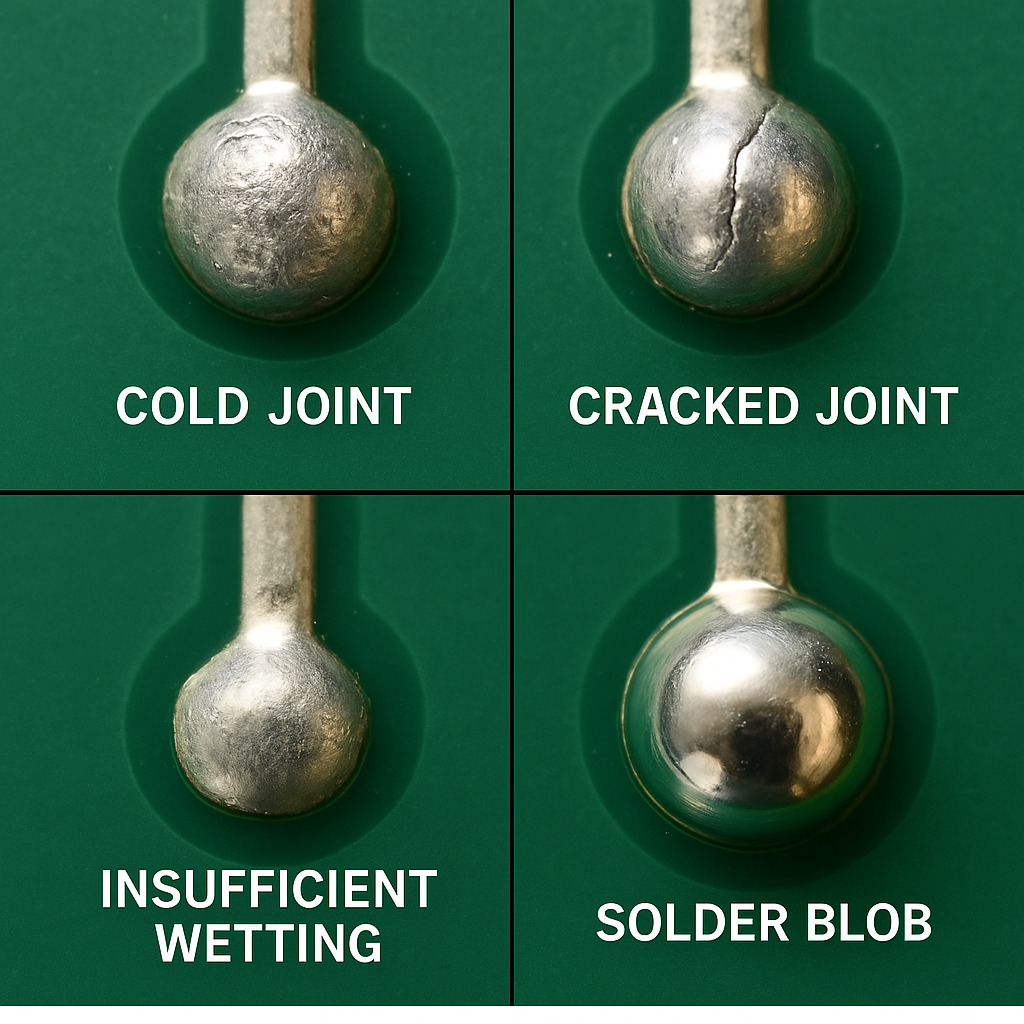
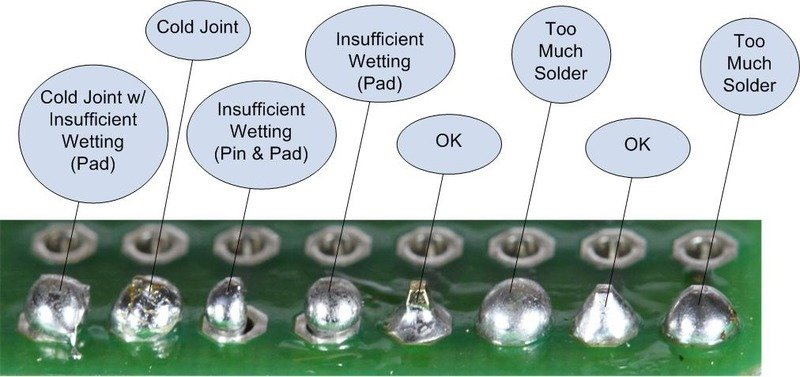
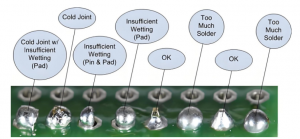
Good soldering also requires clean surfaces, stable temperature control, and adequate flux. Rushing the process leads to cold joints or weak bonds.
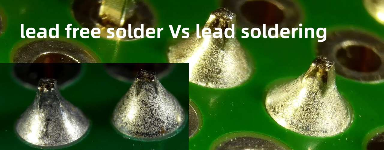
A reliable solder joint shows smooth fillets, full wetting, and consistent shine. These visual cues reflect sound metallurgical bonding, not just appearance.
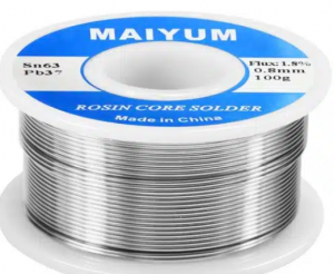
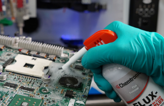
What Is the Best Flux for Through-Hole Soldering?
Choosing the right flux improves through hole soldering quality and repeatability. Flux removes oxidation and promotes solder flow.
For most electronic assemblies, no-clean flux is widely used. It leaves minimal residue and simplifies post-solder cleaning. Rosin-based flux offers strong activity but may require cleaning.
Water-soluble flux provides excellent wetting but demands thorough rinsing. It is often used in controlled environments with established wash processes.
The best flux depends on the soldering method, board material, and reliability requirements. Manufacturers like EBest Circuit (Best Technology) select flux types based on assembly complexity and end-use standards.
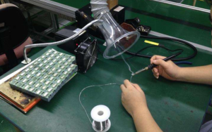
Can You Hand Solder a Surface Mount?
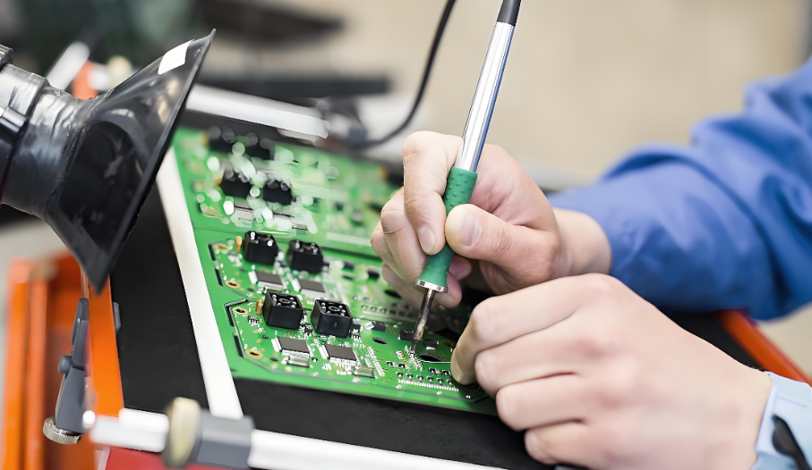
Yes, you can hand solder surface mount components. While SMT is designed for automation, skilled technicians routinely hand solder prototypes, repairs, and small batches.
The process requires fine tips, steady temperature control, and magnification. Proper flux application makes a significant difference in wetting and joint quality.
Hand soldering works best for larger surface mount packages such as SOIC, QFN, and discrete passives. Very fine-pitch devices demand more experience.
What Is the Most Common Problem With Soldering?
The most common problem with soldering is insufficient wetting. This issue affects both surface mount vs through hole soldering.
Poor wetting occurs when solder fails to bond smoothly to the pad or lead. Causes include contamination, low temperature, or inadequate flux.
Other frequent issues include solder bridges, voids, and uneven fillets. These problems are preventable with process control and inspection.
Conclusion:
Understanding through hole vs surface mount is about matching technology to function. Surface mount technology supports compact, high-speed, and high-volume electronics. Through hole technology delivers strength, durability, and dependable power handling.
EBest Circuit (Best Technology) works closely with customers to select the right combination of surface mount and through hole processes. If you have questions about component selection, soldering methods, or mixed-technology PCBA projects, professional guidance can save time and reduce risk.
For technical inquiries or sourcing support, please contact sales@bestpcbs.com