Struggling to understand how consigned PCB assembly differs from turnkey and which one saves you money? This guide compares definitions, costs, service scopes, lead times, risks, and supplier choices to help you optimize your PCB decisions efficiently.
What is Consigned PCB Assembly?
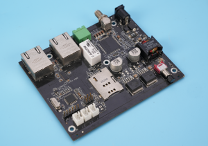
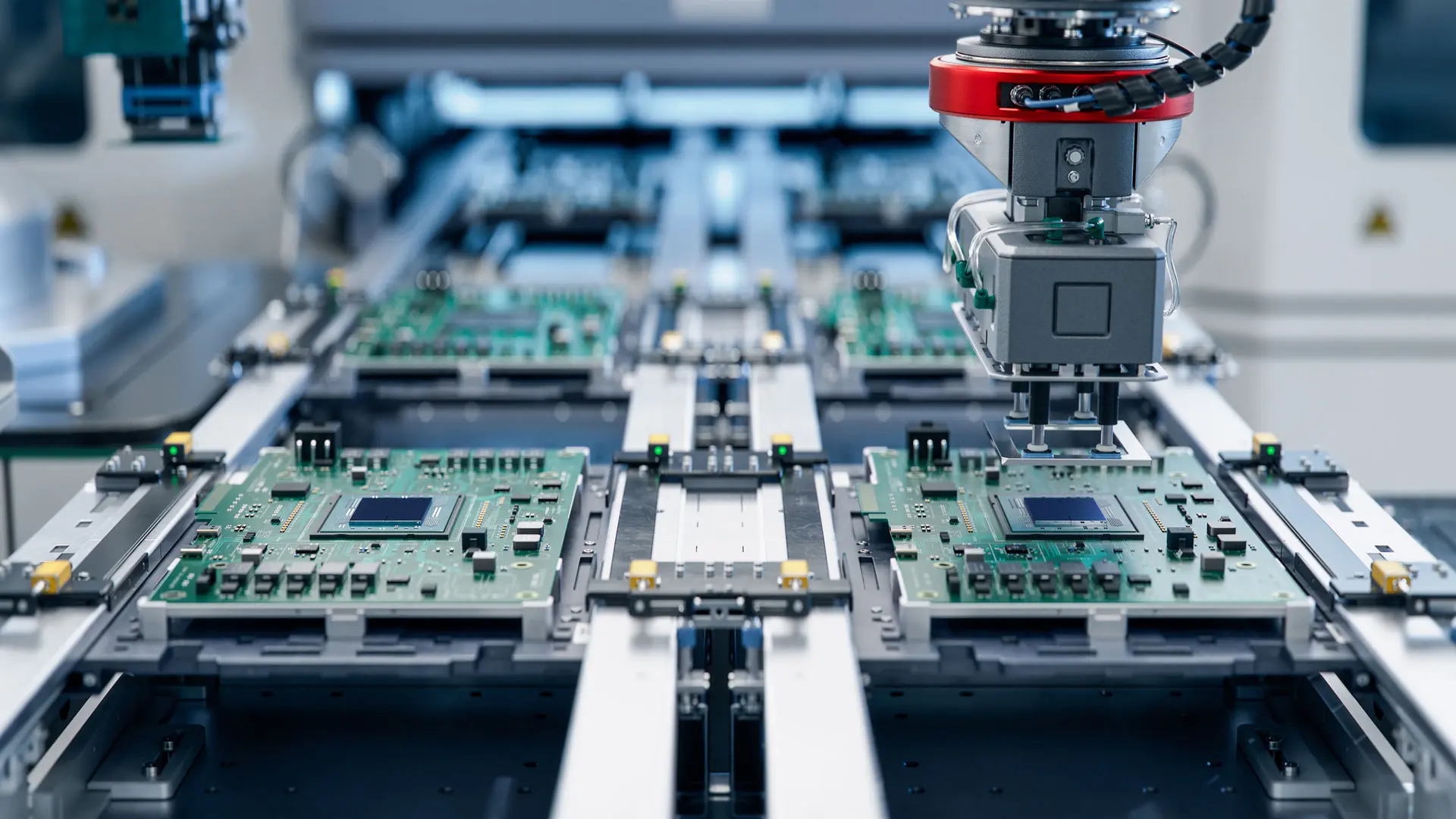
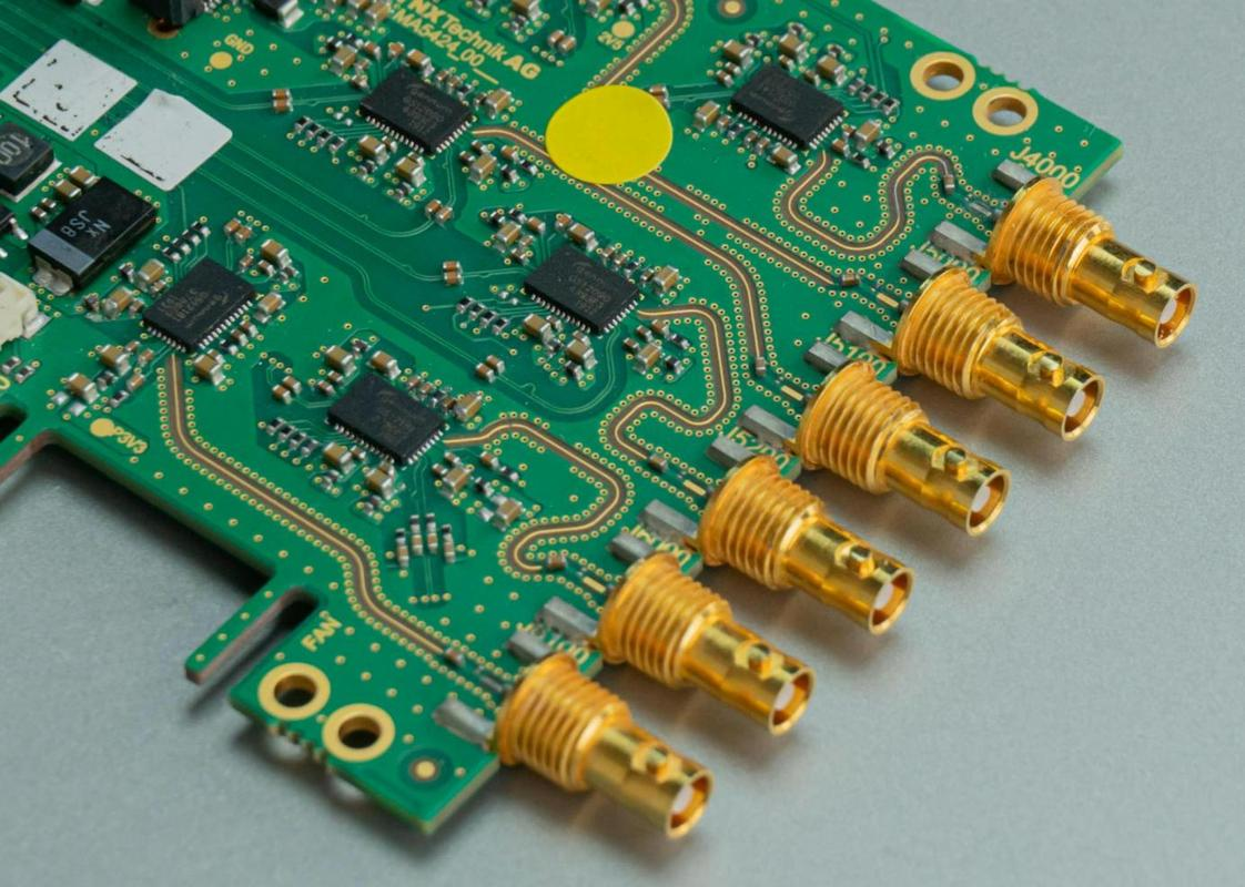
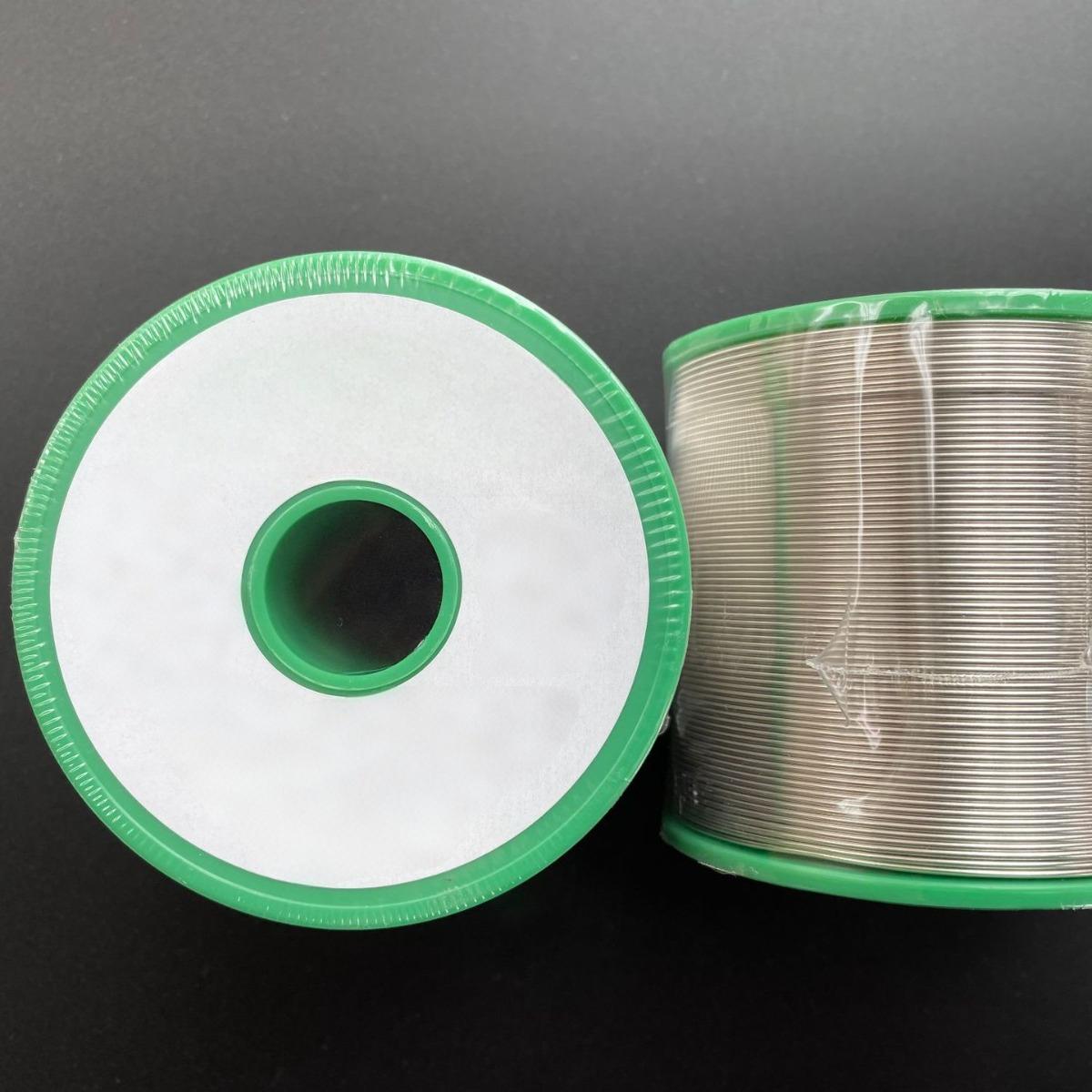
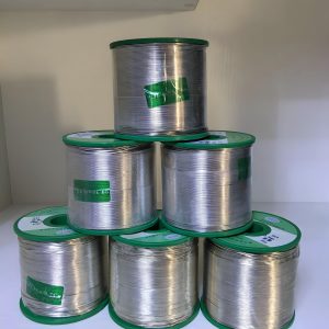
Consigned PCB assembly refers to a service where the client provides all necessary components (such as resistors, capacitors, ICs, and PCBs), and the manufacturer is responsible for assembling these components into finished PCBs according to the client’s specifications. This model puts the client in control of component sourcing, while the manufacturer handles the assembly process, quality testing, and packaging.
A reputable consignment PCB assembly supplier will verify component quality upon receipt, ensure proper storage to prevent damage, and follow strict assembly protocols to meet the client’s requirements. This model is ideal for clients who have established component supply chains or need to use specific, high-quality components for their products.
What is Turnkey PCB Assembly?
Turnkey PCB assembly is a full-service solution where the manufacturer takes complete responsibility for the entire PCB production process. This includes component sourcing, procurement, assembly, testing and delivery. Clients only need to provide the design files (Gerber files, BOM list) and specifications, and the manufacturer handles the rest.
This model eliminates the need for clients to manage component sourcing. It reduces administrative burdens and potential supply chain risks, making turnkey solutions popular among businesses that want to streamline their production process and focus on core operations instead of component management.
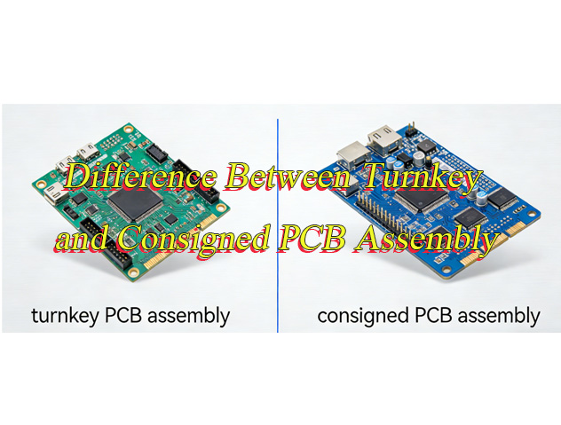
Difference Between Turnkey and Consigned PCB Assembly
| Comparison Aspect | Turnkey PCB Assembly | Consigned PCB Assembly |
| Material Procurement | Manufacturer handles all component sourcing | Client supplies components |
| Cost Structure | Higher upfront cost but lower total cost (bulk buying, logistics savings) | Lower material costs but higher management/labor costs |
| Lead Time | Typically shorter (manufacturer controls supply chain) | Varies based on client’s supply chain efficiency |
| Risk Allocation | Manufacturer bears sourcing/quality risks | Client bears component quality/supply risks |
| Quality Control | Manufacturer-managed (integrated process) | Shared responsibility (client controls part quality) |
| Flexibility & Customization | Limited (predefined specs) | High (client can modify materials/processes) |
| Volume Efficiency | Optimal for large-scale production | Better for small batches/specialty items |
| Client Expertise Required | Minimal (relies on manufacturer) | High (requires sourcing/inventory management skills) |
| Supply Chain Control | Manufacturer-managed | Client-controlled |
| Total Cost of Ownership | Often lower (logistics/bulk savings offset fees) | Potentially higher (inventory/management costs) |
Cost Analysis: Is Consigned PCB Assembly More Economical for Small Businesses?
For international small businesses, cost control directly affects operational sustainability. Unlike turnkey solutions, consigned PCB assembly eliminates manufacturer sourcing markups, cutting direct costs significantly. This is a game-changer for budget-conscious small businesses, especially those leveraging regional trade agreements, as sourcing components locally or from preferential regions can slash tariff costs by up to 60% in some cases, and you retain full control over component pricing to negotiate bulk discounts with trusted suppliers, critical for reducing per-unit costs on small to medium production runs.
However, hidden costs can erode savings if you lack an established component supply chain. These include international shipping fees, customs delays, and rework costs from low-quality components; for example, urgent component shipping or rework for defective parts can add 15-30% to your total costs, negating initial assembly savings from consigned services, especially when navigating complex global trade rules and supply chain gaps.
The key to cost efficiency lies in your component supply chain: if you have reliable local or regional component suppliers, consigned PCB assembly is almost always more economical, as it avoids turnkey markup and lets you optimize tariffs and component costs. Without trusted suppliers, turnkey may be cheaper, as manufacturers leverage global networks to secure components at lower costs and avoid hidden supply chain expenses, including those associated with international shipping and compliance checks.
Service Scope Comparison: Consigned vs. Turnkey PCB Solutions
Understanding the exact services included in each assembly model helps you choose the right fit for your global operations. Both options focus on quality and efficiency but differ significantly in the level of support provided, especially for international clients managing cross-border supply chains.
Consigned PCB Assembly Services
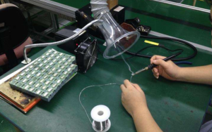
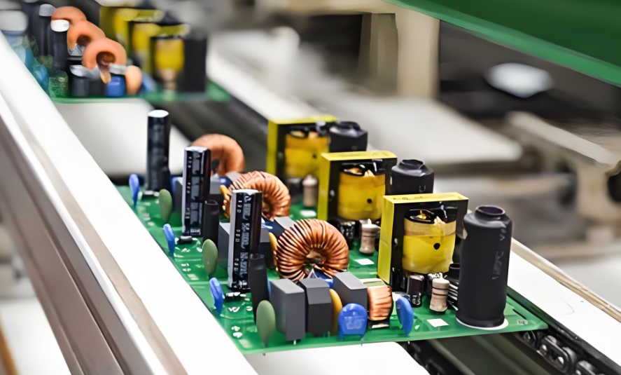
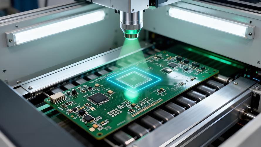
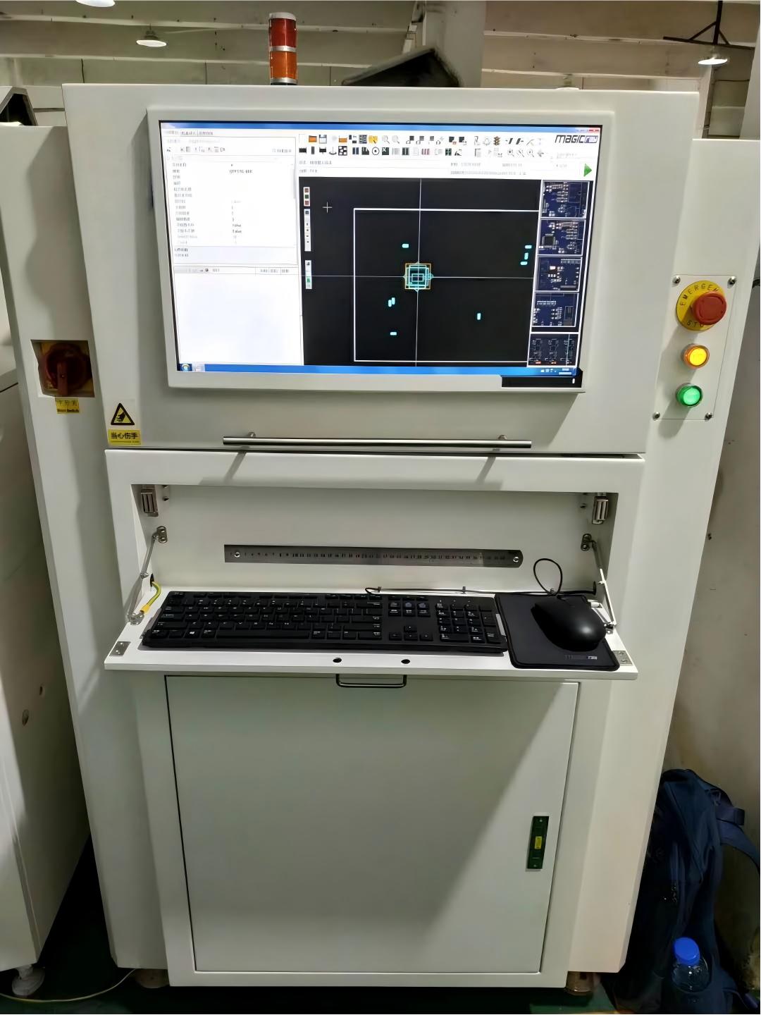
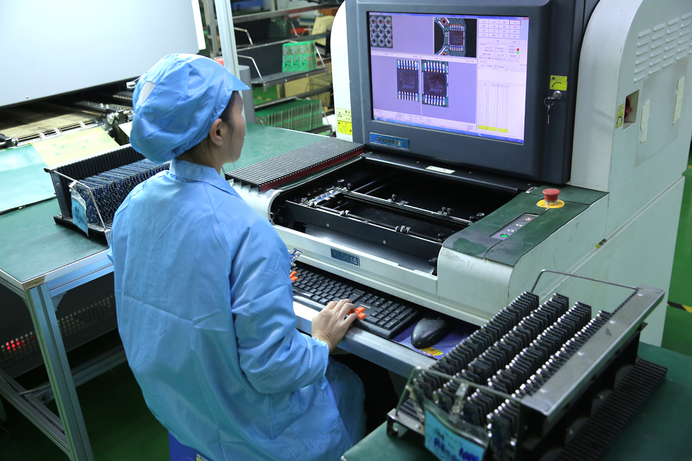
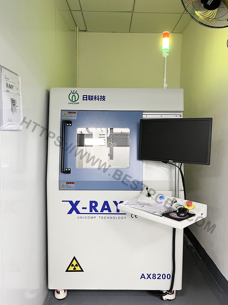
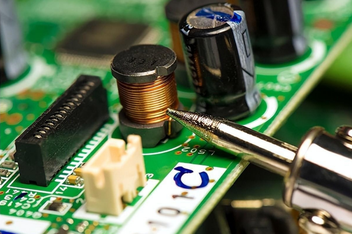
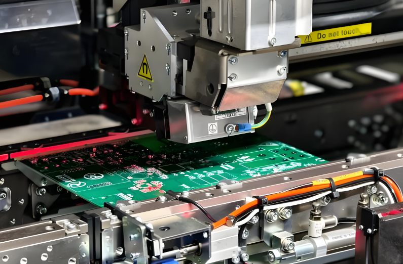
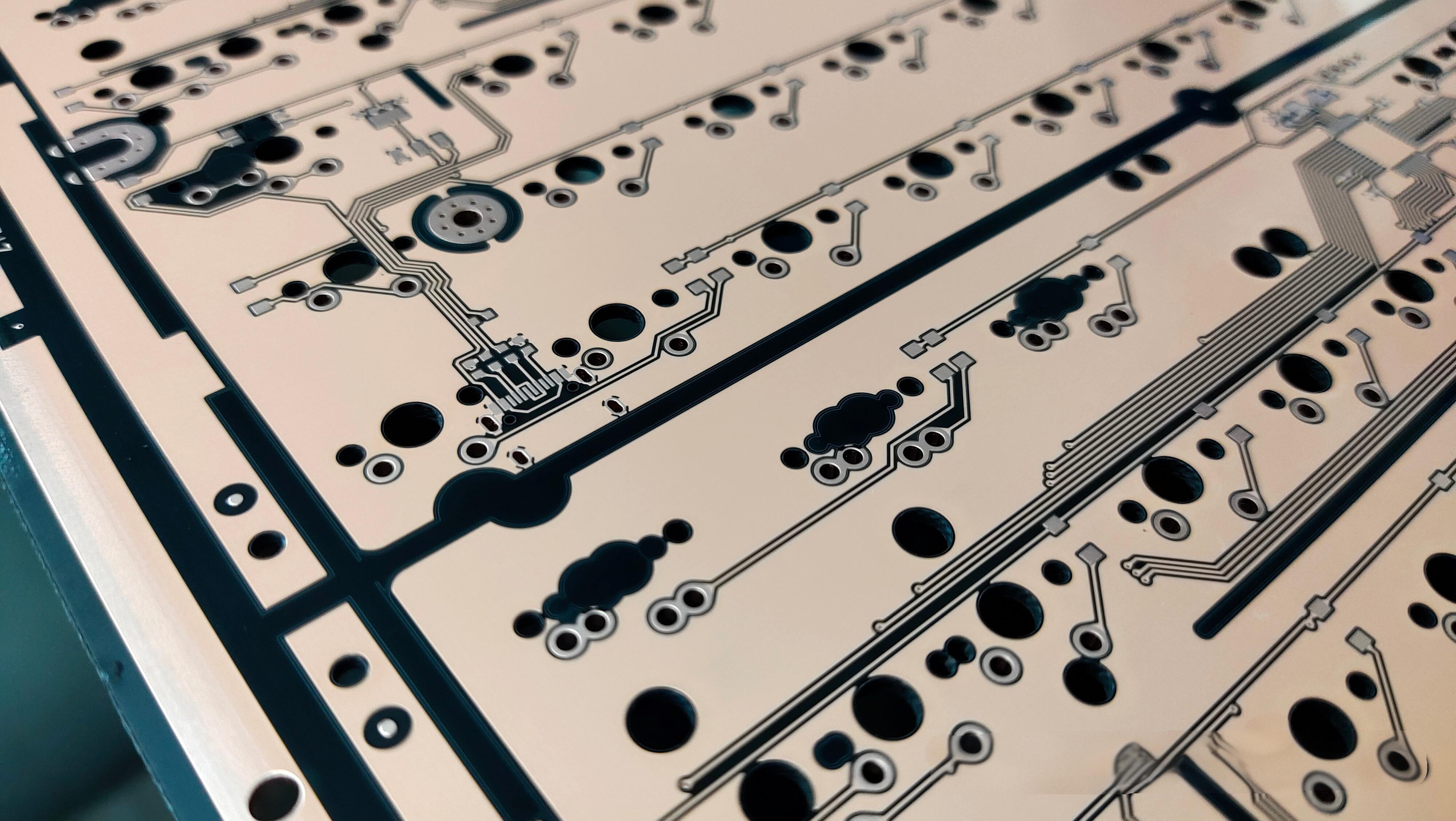
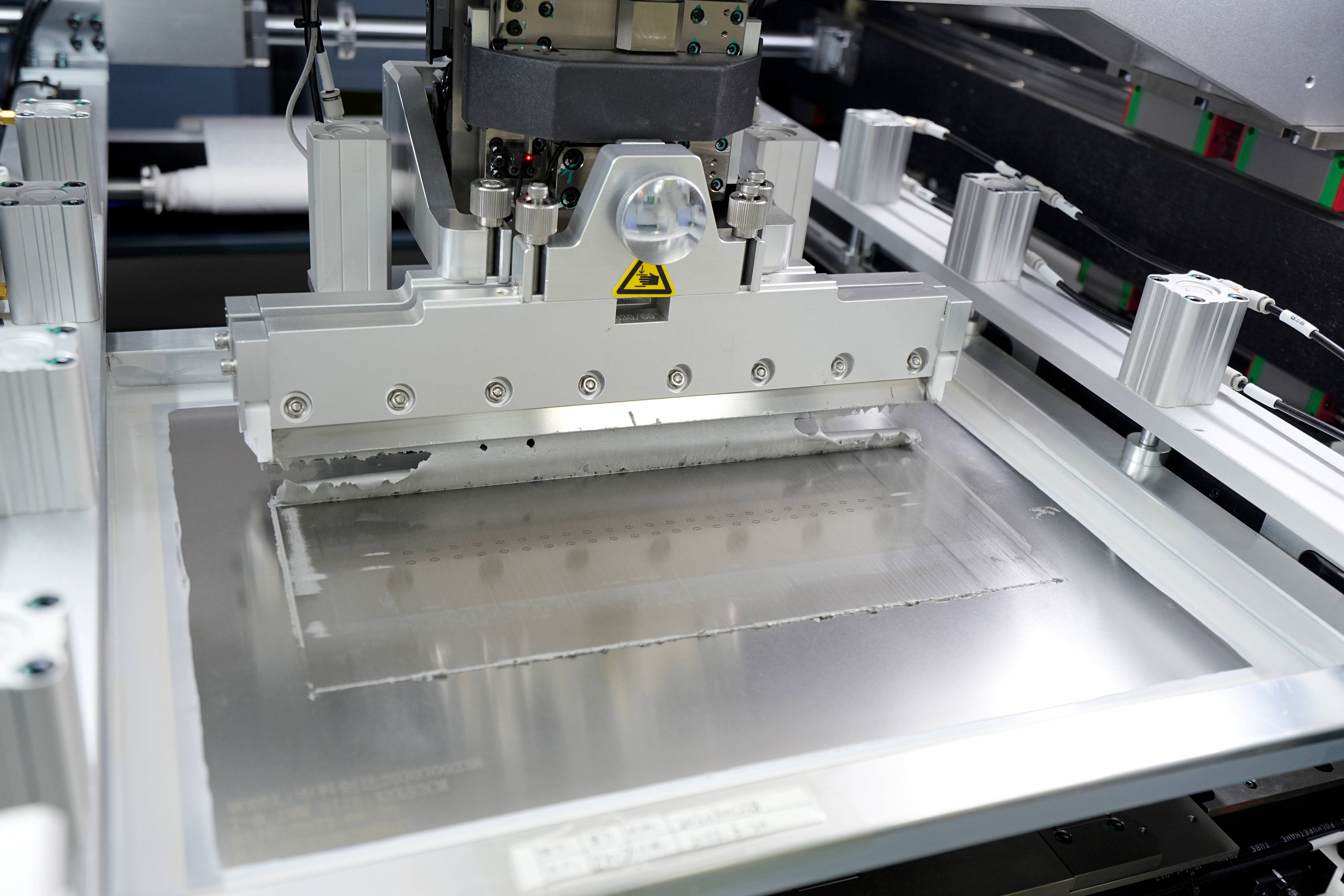
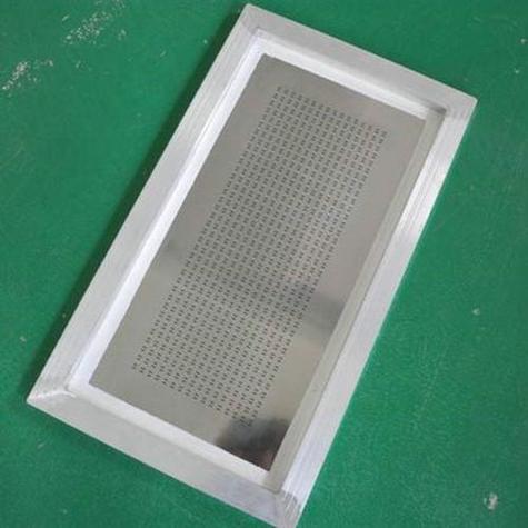
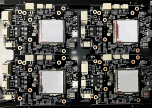
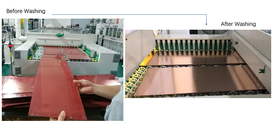
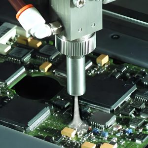
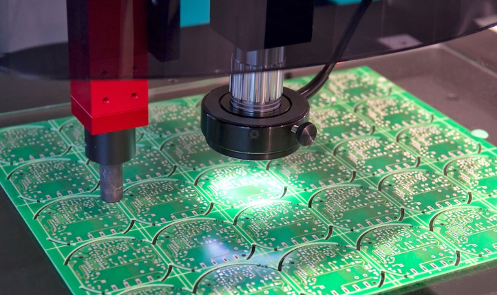
Consignment PCB assembly services are tailored for clients who want control without sacrificing quality. Key services include component inspection to verify your parts meet specifications, SMT and through-hole assembly, rigorous testing such as AOI, X-ray and functional testing, and packaging optimized for international shipping. Many suppliers also offer component storage so you can stage parts for ongoing production and avoid repeated international shipping costs.
This model keeps you in charge of component sourcing while we handle the technical aspects of assembly. It is ideal for clients with established supplier relationships who want to maintain consistency across global production batches.
Turnkey PCB Solutions
Turnkey solutions are designed for international clients who want to simplify their supply chain. They include all consigned assembly services plus component sourcing with compliance checks for regional standards like EU RoHS and US FCC, DFM analysis to optimize designs for global production, inventory management, and global shipping with end-to-end tracking. This eliminates the need to coordinate with multiple suppliers and customs agents.
Turnkey services leverage the manufacturer’s global supplier networks and logistics expertise to streamline your operations. They are perfect for clients new to global manufacturing or those looking to reduce administrative workload and supply chain complexity.
Lead Time Efficiency: Can Consigned PCB Assembly Beat Turnkey for Urgent Deadlines?
Yes, consigned PCB assembly is significantly more efficient for meeting urgent global deadlines, especially with same day consigned PCB assembly options. When you provide all necessary components, your manufacturer can begin assembly the moment those parts arrive. This cuts out the 3 to 7 days (or longer) typically needed for component sourcing in turnkey solutions, which is a critical benefit when you’re up against tight market launch timelines or need to quickly replace defective parts for global customers. Many international clients rely on this speed to avoid costly delays that could harm their brand reputation in competitive markets.
For international clients, partnering with a consignment PCB assembly supplier with proven global shipping experience is key to faster turnaround. We’re familiar with customs regulations across major markets from the EU and US to Asia, and use specialized packaging (like vacuum sealing for high-tech PCBs) to prevent damage during transit, which also helps streamline customs inspections and avoid hold-ups. We provide real-time tracking for every shipment, so you can monitor delivery progress at any time. Turnkey solutions, by contrast, often struggle with urgent deadlines because they’re dependent on global component sourcing, which can face delays from supply chain disruptions or customs issues.
Risk Assessment: Consignment vs. Turnkey PCB Assembly
For international clients, understanding the risk differences between consigned and turnkey PCB assembly is critical to protecting your business, brand reputation, and bottom line. Each model shifts risk responsibility differently, and knowing these nuances helps you choose the option that aligns with your risk tolerance and operational capabilities.
Consigned PCB Assembly Risks
With consigned PCB assembly, the majority of supply chain risks fall on you, the client. This is a key tradeoff for the control you gain over component sourcing and quality.
The most common risks include component shortages caused by global supply chain disruptions, damage to parts during international shipping, and the threat of counterfeit components if your suppliers are not reputable. Counterfeit parts are particularly dangerous as they can fail unexpectedly, damage your products, and even harm your brand’s credibility in global markets.
You also bear the risk of non-compliant components. If the parts you source do not meet regional standards like EU RoHS or US FDA, your finished products may be rejected at customs, leading to costly delays and rework.
To mitigate these risks, partner with a consignment PCB assembly supplier that conducts thorough component inspections upon receipt, offers climate-controlled storage to prevent damage, and provides detailed quality reports. This ensures your components meet the standards required for your target markets and reduces the chance of costly errors.
Turnkey PCB Assembly Risks
In turnkey PCB assembly, most supply chain and quality risks shift to the manufacturer, relieving you of the administrative burden but requiring trust in your partner’s capabilities.
The primary risks the manufacturer bears include sourcing counterfeit or non-compliant components, unexpected component price fluctuations, and supply chain delays due to global events or part shortages. These issues can delay your order and impact your ability to meet market deadlines.
While the manufacturer takes on most risks, you still face potential setbacks if they fail to meet your quality or delivery requirements. Poor assembly quality or missed deadlines can disrupt your operations and damage relationships with your own customers.
To minimize these risks, choose a turnkey supplier with a proven track record of serving international clients, transparent sourcing processes, and strict compliance with global standards (IPC-610, RoHS, FCC). A reliable supplier will also offer DFM analysis to prevent design-related risks and ensure smooth production.
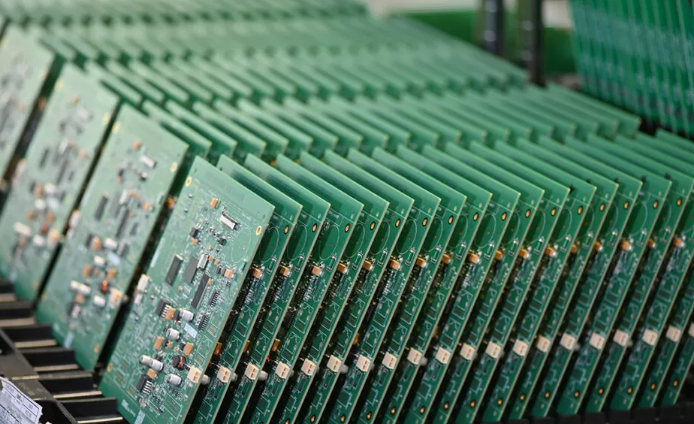
Volume Strategy: Why Choose Consigned PCB Assembly for High-Volume Production?
Consigned PCB assembly offers strategic advantages for high-volume production by prioritizing client control over costs, quality, and supply chain flexibility. Below is a structured breakdown of its benefits, tailored to client priorities:
- Cost Efficiency Through Direct Component Sourcing: Clients avoid manufacturer markups (typically 5–20%) and inventory overhead by supplying components directly. This model is ideal for companies with pre-negotiated supplier contracts or access to bulk/specialized components. For example, projects leveraging long-term supplier deals can achieve 15–40% cost savings compared to turnkey solutions. High-volume runs benefit from bulk purchasing efficiencies, reducing per-unit costs significantly.
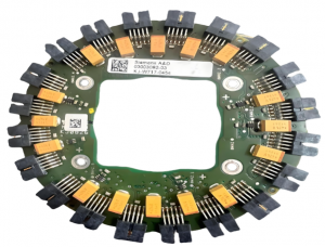
- Enhanced Quality Control: Clients retain full oversight of component quality, ensuring adherence to standards like IPC-A-610. Automated inspection tools (SPI, AOI, X-ray) detect early-stage anomalies and soldering defects, ensuring consistent quality across thousands of boards. This is critical for reliability-driven industries (e.g., automotive, telecommunications), where field failures carry high costs.
- Supply Chain Agility & Risk Mitigation: Consigned assembly shifts supply chain management to the client, avoiding delays from third-party logistics or supplier shortages. Clients with robust in-house supply chains can coordinate component deliveries directly, ensuring timely production starts. This model also mitigates risks like component obsolescence or price fluctuations, as clients proactively manage inventory lifecycles and source alternatives.
- Customization for Specialized Components: For projects requiring niche, patented, or custom-designed components, consigned assembly allows direct integration without manufacturer constraints. This is particularly valuable for R&D-driven or niche products where component specifications must align precisely with design goals. Manufacturers focus on assembly expertise, while clients handle specialized sourcing.
- Accelerated Time-to-Market: High-volume production demands rapid scaling. Consigned assembly reduces lead times by eliminating the need for manufacturer-led component procurement. Clients with pre-sourced components can initiate assembly immediately, leveraging contract manufacturers’ (CMs) high-speed SMT lines for quick-turn delivery (e.g., 2–4 days for QuickTurn services). This agility is crucial for meeting tight deadlines and capitalizing on market opportunities.
Selection Criteria: Consignment vs. Turnkey PCB Assembly Supplier
When selecting a consignment PCB assembly supplier for global production, prioritize these factors:
- Component Sourcing Control: For consigned PCB assembly, you provide all components, keeping full control over quality, sourcing channels, and regional compliance (e.g., EU RoHS, US FDA). For turnkey, the manufacturer sources all components via their global network, handling counterfeit risk and compliance checks.
- Cost & Tariff Efficiency: Consigned has lower direct assembly fees (no sourcing markup) but requires you to manage component costs and optimize local tariffs. Turnkey includes a component markup but leverages bulk sourcing to lower total costs, with the manufacturer handling tariff optimization across regions.
- Lead Time for Urgent Orders: Consigned delivers faster once components arrive, supporting same-day consigned PCB assembly for tight deadlines (cuts out 3–7 days of sourcing). Turnkey has longer lead times due to sourcing, making it harder to meet urgent deadlines.
- Risk Distribution: In consigned, you bear supply chain risks (shortages, counterfeits, shipping damage). In turnkey, the manufacturer takes most sourcing risks, leaving you only at risk of delivery delays from the manufacturer.
- Service Scope Fit: Consigned focuses on assembly, testing (AOI, X-ray, functional), packaging, and component storage, ideal if you already have trusted suppliers. Turnkey offers end-to-end support: sourcing, DFM analysis, inventory, and global shipping, perfect for simplifying your supply chain.
- Volume Suitability: Consigned works best for high-volume production to leverage bulk component discounts and ensure stable global supply. Turnkey is cost-effective for low-to-medium volumes or small batches, avoiding the need for large component stockpiles.
- Quality & Compliance Assurance: Consigned relies on your component compliance; the manufacturer ensures assembly meets IPC-610 standards. Turnkey covers component and assembly compliance, including DFM analysis to prevent design-related production issues.
- Supplier Selection Criteria: For consigned, pick suppliers with strong component inspection, climate-controlled storage, and 24/7 English communication to handle global time zones. For turnkey, prioritize a large authorized supplier network, compliance expertise (ISO 9001, RoHS), and transparent pricing.
Conclusion
At the end of the day, the choice between consigned PCB assembly and turnkey PCB assembly boils down to your business’s unique needs, resources, and priorities, especially as the global PCB industry enters a new growth cycle driven by AI and automotive innovation. If you have trusted global component suppliers, prioritize control over quality and compliance, need fast turnaround for urgent orders, or handle high-volume production for global markets, consigned assembly is your ideal fit. For businesses seeking to simplify their supply chain, lacking established component sources, or working with low-to-medium volumes, turnkey assembly offers the convenience and peace of mind to focus on your core growth.