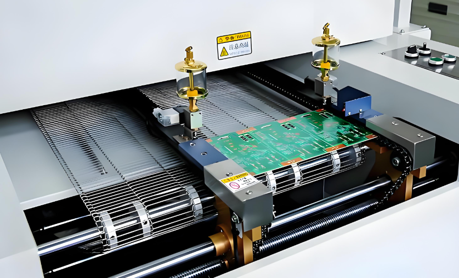
EMS refers to a range of services offered by specialized companies that design, assemble, test, and distribute electronic components or assemblies. These services are crucial to the electronics supply chain, especially as companies seek faster production, cost-effective solutions, and greater focus on innovation rather than internal manufacturing processes. In this article, we will explain the EMS meaning in electronics, how it differs from OEM, and why it’s becoming the preferred solution for many industries.
What Does EMS Stand for in Electronics?
In electronics, EMS stands for Electronic Manufacturing Services. It describes companies that offer a full range of manufacturing services for electronic products on behalf of original equipment manufacturers (OEMs). EMS companies handle everything from printed circuit board assembly (PCBA) to box builds, testing, and even logistics.
The EMS meaning in electronics has evolved over the years. Initially focused only on assembly, EMS now covers the entire product lifecycle, including design assistance, prototyping, materials sourcing, final product integration, and post-sales services. EMS helps companies reduce production costs, improve lead times, and maintain high-quality standards without building their own manufacturing facilities.
What Is the Difference Between OEM and EMS?
Many people confuse OEM (Original Equipment Manufacturer) with EMS, but they serve very different purposes.
An OEM is responsible for the product concept and design. OEMs usually create the brand, own the intellectual property (IP), and manage marketing and distribution. However, they often outsource the actual manufacturing to EMS providers.
An EMS company specializes in manufacturing electronics based on the OEM’s design. They may offer additional services such as design optimization and testing, but they don’t usually own the product IP.
For example:
A tech startup designs a wearable fitness tracker. They are the OEM. Instead of setting up a factory, they work with an EMS provider to manufacture the product, conduct functional testing, assemble the final unit, and ship it globally.
What Do EMS Providers Do?
EMS providers offer a full suite of services that span from initial design consultation to final product shipment. These services typically include:
PCB assembly (SMT & THT)
Sourcing of electronic components
Design for manufacturing
Engineering Support
Prototype service
Testing and inspection (ICT, FCT, AOI, X-RAY, etc.)
Mechanical assembly
Box build and system integration
Packaging and logistics (depends on the payment terms)
EMS companies play a central role in bridging the gap between product design and final delivery. Businesses that don’t own manufacturing plants—or wish to scale quickly—can rely on EMS companies to handle production, logistics, and even after-sales support.
Common Industries That Rely on EMS Solutions
Many industries especially for electronic industry depend on EMS companies due to the complex nature of electronic product development and production. Some common industries include:
1. Consumer Electronics
Smartphones, tablets, wearables, and gaming consoles are often produced in partnership with EMS companies, who manage high-speed assembly and short product lifecycles.
2. Medical Devices
From diagnostic equipment to portable health monitors, EMS companies provide precision assembly and documentation that comply with strict medical regulations (e.g., ISO13485).
3. Automotive Electronics
Modern vehicles are full of electronic control units (ECUs), infotainment systems, sensors, and cameras. EMS partners help automakers achieve reliability and consistency.
4. Telecommunications
Routers, base stations, and networking equipment require robust PCBA and quick scalability—ideal for EMS manufacturing models.
5. Industrial Automation
Controllers, PLCs, and robotics equipment are often built by EMS providers, ensuring durability and performance in tough environments.
Benefits of Working with EMS Companies
Working with EMS companies brings many advantages, especially for businesses looking to optimize operations and reduce overhead.
1. Cost Reduction
EMS providers work at scale, reducing material costs, labor expenses, and production waste. Their optimized processes bring significant cost savings compared to in-house manufacturing.
2. Faster Time to Market
EMS companies are built for speed. They streamline procurement, assembly, and testing, helping OEMs launch products more quickly.
3. Production Flexible
Whether you’re building 100 units or 100,000, EMS providers can ramp up production based on your needs.
4. Access to Skilled Labor and Advanced Equipment
With a dedicated team of engineers, technicians, and quality experts, EMS partners ensure high-quality output using modern equipment.
5. Reduced Supply Chain Complexity
EMS providers handle sourcing, logistics, and inventory management, reducing the burden on the OEM and improving reliability.
6. Global Reach
Some EMS companies offer local manufacturing as well as global distribution, making it easier to reach customers worldwide.
Electronic Manufacturing Services (EMS) Companies in China
China is home to some of the world’s most established electronic manufacturing services providers. These companies support global clients by offering:
Competitive pricing
Fast turnaround
Mature supply chains
Skilled engineering teams
High-volume production capabilities
Whether it’s smartphones, industrial controllers, or IoT devices, many companies prefer to work with electronic manufacturing services (EMS) companies in China for their ability to handle rapid prototyping, complex assembly, and scalable production.
Chinese EMS companies often provide end-to-end solutions—from prototyping to full product assembly—and are favored by startups and global brands alike. Some common PCB EMS provider like:
PCBWay
JLCPCB
EBest Circuit (Best Technology)
ALLPCB
Hitech Circuits Co., Ltd.
NextPCB
Rayming PCB
Why EBest Circuit (Best Technology) Is a Trusted EMS Partner?
EBest Circuit (Best Technology) is a professional EMS provider based in China, offering complete manufacturing services to clients worldwide. We are committed to delivering reliable, high-quality electronics tailored to customer requirements.
We are certified to ISO9001, ISO13485, IATF16949, AS9100D, UL, RoHS, ensuring that every product meets global quality standards.
From PCB fabrication to final assembly and logistics, we provide turnkey EMS solutions that shorten lead times and reduce complexity.
Our experienced team helps optimize your designs for better performance and lower production costs.
With strong supply chain relationships and efficient production methods, we offer fair pricing without compromising quality.
We serve clients in North America, Europe, and Asia, with strong communication and technical support.
Whether you need rapid prototypes or high-volume manufacturing, EBest Circuit (Best Technology) is ready to be your trusted EMS partner.
FAQs
1. What is EMS meaning in electronics?
EMS stands for Electronic Manufacturing Services. It refers to companies that manufacture, assemble, and test electronic components or systems for other businesses.
2. How is EMS different from OEM?
OEMs design and brand products, while EMS companies focus on manufacturing and assembly based on OEM specifications.
3. Why do businesses prefer EMS providers?
EMS partners help reduce cost, speed up product launches, and allow companies to focus on design and sales instead of manufacturing.
4. Are EMS companies only for large corporations?
No. Many small and medium-sized businesses rely on EMS companies for prototyping, small-batch runs, and full production.
5. What makes EBest Circuit (Best Technology) a reliable EMS company?
EBest Circuit (Best Technology) offers certified quality, full traceability, engineering support, and turnkey EMS solutions backed by years of experience in the industry.
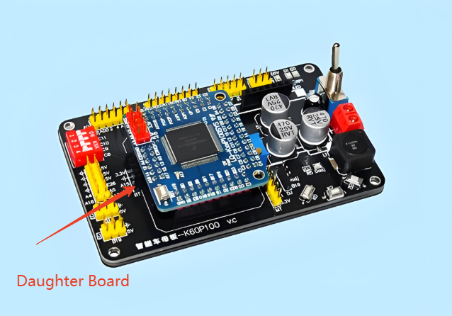
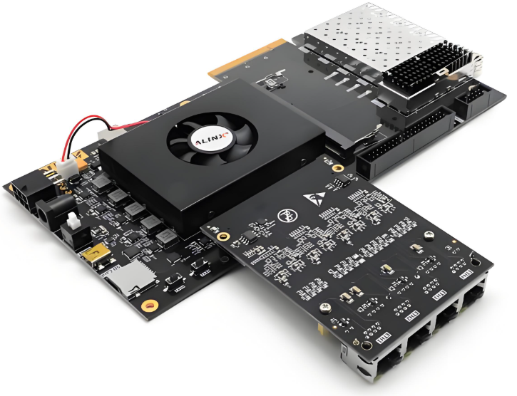
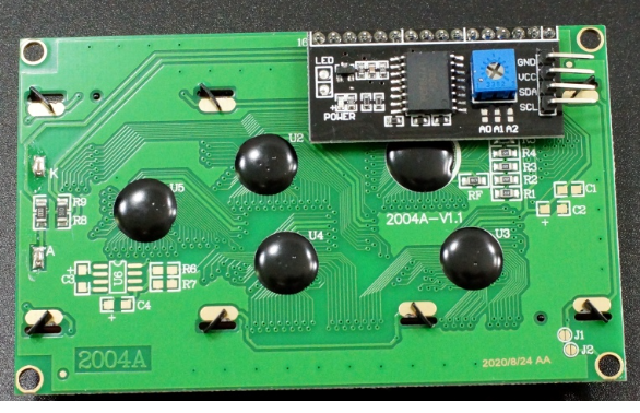
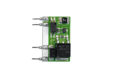
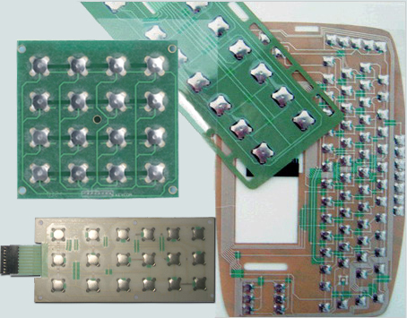
Daughter board is a term you might hear often when dealing with modular or expandable electronics. Whether you’re working on an industrial control system or building a custom computing platform, daughter boards play an essential role in modern circuit design. They provide a flexible way to add functions without reworking the main PCB. In this blog, we’ll explain what a daughter board is, how it compares to a motherboard, where it’s used, and how you can design or source one with support from EBest Circuit (Best Technology).
What Is a Daughter Board?
A daughter board is a secondary printed circuit board (PCB) that connects to a larger mainboard or motherboard to expand the system’s functions. Think of it as an add-on card or module. It doesn’t work alone but works in combination with a central PCB. It often contains components such as integrated circuits, connectors, sensors, or specialized chips.
These boards are commonly used when the system needs modular features, like upgrading ports, adding wireless capabilities, or supporting additional I/O. For example, in a test system, you might use one daughter board for analog inputs and another for digital outputs.
What Is Another Name for a Daughter Board?
Daughter boards are known by different names depending on their role or industry. Some common synonyms include:
Daughter card
Mezzanine board
Add-on board
Expansion board
Piggyback board
All these terms describe the same core idea—a smaller board that connects to and works with a larger one.
Types of Daughter Boards
Daughter boards come in many forms, each built to serve a particular function. They help expand the capabilities of the mainboard while keeping the system modular and easier to maintain. Here are the most common types used in computing, electronics, and industrial applications:
1. RAM DIMMs (Dual Inline Memory Modules)
RAM DIMMs are one of the most recognized daughter boards used in computers. These modules plug directly into designated memory slots on the motherboard. Their job is to increase a system’s memory capacity, allowing it to handle more data and run applications smoothly.
In modern computing, larger RAM is essential for multitasking, video editing, gaming, and server operations. DIMMs come in different sizes and speeds—such as DDR4 and DDR5—and are easily replaceable. Without them, most systems would be stuck with limited onboard memory, which slows down performance.
2. Storage Expansion Boards
Storage expansion boards provide extra connections for drives like HDDs (Hard Disk Drives) or SSDs (Solid-State Drives). These daughter boards offer additional interfaces such as SATA, NVMe, U.2, or M.2 that might not be available on the motherboard.
Some advanced boards also include built-in RAID support, which protects data by mirroring or distributing it across multiple drives. These are especially useful in servers, data centers, and high-performance computing where fast and reliable storage is a top priority.
3. Graphics Cards (GPUs)
Graphics cards are powerful daughter boards that handle video output and image rendering. They connect through slots like PCIe and often come with their own processors, memory, and cooling systems. This makes them ideal for graphic-intensive applications such as gaming, animation, 3D rendering, and AI computations.
A dedicated GPU offloads tasks from the CPU, significantly improving performance in systems that need to display complex visuals. While some basic systems use integrated graphics, most high-performance setups depend on discrete GPU daughter boards.
4. Network Interface Cards (NICs)
Network Interface Cards are daughter boards that enable wired or wireless network connectivity. While many modern motherboards come with built-in Ethernet or Wi-Fi, NICs are still widely used for upgrading to higher-speed interfaces (such as 10GbE) or adding more ports.
These boards are commonly found in servers, workstations, and gaming systems. In industrial applications, NICs may support fiber optics, PoE (Power over Ethernet), or advanced features like VLAN tagging and network booting.
5. Audio Processing Boards
Audio daughter boards process sound input and output. Unlike basic onboard audio systems, these specialized boards use high-quality digital-to-analog converters (DACs), pre-amplifiers, and noise filters to deliver clearer, richer audio.
They are widely used in music production, live broadcasting, home theater setups, and gaming rigs. Some also support surround sound formats and professional studio interfaces. If audio quality is critical to your application, a dedicated audio processing board is a valuable upgrade.
6. Display Interface Boards
Display interface boards handle video signal conversion and output for external screens. These daughter boards may include HDMI, VGA, DVI, DisplayPort, or LVDS connectors. In embedded systems, you may also find boards designed to interface directly with LCD or OLED panels.
They are commonly used in digital signage, kiosks, medical imaging devices, and control panels where display requirements vary. By offloading display functions to a daughter board, designers can support multiple screen types without changing the mainboard.
7. Power Regulation Boards
Power regulation boards manage how power is distributed and controlled in an electronic system. They often perform tasks such as voltage step-down/up, current limiting, charging, or power sequencing. These daughter boards are important in devices that require multiple voltage rails or battery management.
In portable devices, these boards ensure efficient use of power while protecting sensitive circuits. In larger systems, they may provide isolation between different zones or convert AC to DC. By moving these functions off the mainboard, designers save space and improve thermal performance.
8. Customization Boards
Customization boards, also known as breakout boards or feature boards, are developed for specific functions that aren’t supported by standard modules. These may include:
Touchscreens and user interface buttons
Sensor modules for temperature, humidity, gas, or motion
GPS, GSM, or LoRa communication modules
Data acquisition boards for test systems
Engineers often design these boards for quick testing, prototyping, or low-volume applications where flexibility is key. They offer a fast and affordable way to add new features without redesigning the whole system.
What Is the Function of a Daughter Board?
The primary function of a daughter board is to provide additional features or functionality to a mainboard. Here are some specific functions it can serve:
Add new sensors or interfaces
Upgrade or replace audio/video output
Provide motion or location tracking
Manage specific voltage domains
Extend computing power with co-processors
Act as a debugging or testing interface
Instead of placing all features on one large board, designers break them up into smaller, modular boards. This approach saves space, simplifies design updates, and reduces cost for future upgrades.
What Is the Difference Between a Motherboard and a Daughterboard?
The motherboard is the main printed circuit board (PCB) in a device. It acts as the central hub that connects all critical components—such as the CPU, memory, storage, power supply, and input/output interfaces. It handles communication between all subsystems and manages the overall operation of the device.
In contrast, a daughterboard is a secondary PCB that connects to the motherboard to add or enhance a specific function. It cannot work independently. Instead, it extends the capabilities of the mainboard by providing extra features like sound processing, network connectivity, graphics acceleration, or additional input/output ports. Here’s a simple comparison:
Feature
Motherboard
Daughter Board
Role
Core system board
Add-on module
Size
Larger
Smaller
Function
Main processor and system logic
Extended features
Upgrade
Rarely replaced
Easily replaced or upgraded
Examples
PC mainboard, controller board
Audio module, sensor board, NIC
At EBest Circuit (Best Technology), we support both motherboard and daughterboard PCB fabrication. Our team can help you plan, prototype, and produce modular solutions with optimal connector design, layout suggestions, and fast production turnaround.
Daughter Board Price
The cost of a daughter board depends on its design, complexity, and production quantity. Here’s a general pricing guide:
Basic I/O boards (2-layer, few components): $5–$15 each in volume.
Sensor modules or wireless boards: $15–$40 depending on components.
Multilayer signal boards (4–6 layers): $50–$100+ per board.
Prototyping runs (low volume): Higher due to tooling, setup, and test costs.
Factors that affect price:
Board size and layer count
Type of connectors
Components used (standard vs. custom)
Surface finish and solder mask
Quantity ordered
If you’re looking for a cost-effective daughter board PCB, EBest Circuit (Best Technology) can offer you accurate quotes with options to fit your budget.
What Is a Daughter Board Used For?
Daughter boards are used across different industries where customization or modularity is a priority:
1. Industrial automation like sensors, control relays, and communicate with programmable logic controllers (PLCs).
2. Bluetooth or Wi-Fi modules in speakers, smart appliances, and gadgets are often built as daughter boards.
3. Automotive’s ECUs to handle GPS, entertainment, camera feeds, or battery management.
4. In medical devices like portable monitors or scanners, daughter boards add ECG, pulse oximetry, or USB functionality.
5. Aerospace and military, used in systems where functions are split across ruggedized modules for reliability and repair.
How to Install a Daughter Board?
Installing a daughter board is usually simple, but care is required. Follow these steps:
1. Turn off the system power and discharge static from your body by touching a grounded metal surface.
2. Check the orientation of the daughter board. Make sure the connector lines up properly.
3. Press the board gently into the socket or header on the motherboard. Do not force it.
4. Secure it with screws or stand-offs if needed.
5. Turn on the power and check the function through your interface or software.
Use the correct tools and avoid touching exposed pins. Improper installation could cause short circuits or connector damage.
Daughter Board Design Tips
Designing a daughter board may seem straightforward, but it requires careful planning to ensure it connects well with the motherboard, functions reliably, and remains easy to manufacture. Whether you’re building a sensor module, a power board, or a display interface, good design practices can help you avoid problems later in production and testing. Here are some essential design tips to keep in mind:
1. Choose the Right Connector
The connection between the daughter board and motherboard is the most critical part of your design. You’ll need to pick the correct board-to-board connector or interface based on your application.
Consider:
Pin count
Current rating
Pitch and alignment
Mounting method
Use high-quality connectors that are easy to assemble and can tolerate vibration or movement if your system is in a harsh environment.
2. Plan for Mechanical Fit and Mounting
Your daughter board should physically fit into the product enclosure or case. Make sure to:
Define the exact outline dimensions and height of the board.
Avoid component collisions between the daughter board and nearby parts.
Use stand-offs, screws, or plastic clips to secure the board and reduce strain on the connectors.
Align connectors precisely to prevent stress or misalignment during insertion.
A good 3D model of your enclosure and PCB assembly helps catch these issues early.
3. Optimize Signal Routing
Careful trace routing ensures signal integrity, especially for high-speed interfaces. Some tips include:
Short and direct traces between the connector and active components.
Controlled impedance routing for high-speed or differential signals (USB, HDMI, LVDS, etc.).
Keep analog and digital signals separated to reduce interference.
Route ground and power planes to provide a stable return path.
For multi-layer daughter boards, a 4-layer stackup (signal–ground–power–signal) is a good starting point for balanced routing.
4. Manage Power Distribution Carefully
The daughter board may receive power from the motherboard or have its own power input. In either case, power management is crucial:
Use fuses or protection diodes to prevent reverse polarity and short circuits.
Include decoupling capacitors near every IC to filter noise.
Ensure power and ground lines are thick enough to carry the required current.
If different voltage levels are used (e.g., 5V and 3.3V), use voltage regulators or level shifters.
Clear power planning prevents issues like overheating, unstable voltage, or damage to connected boards.
5. Label Everything Clearly
Proper labeling helps with assembly, testing, and future troubleshooting. Best practices include:
Silkscreen component names and pin labels near connectors.
Use clear reference designators (e.g., U1, C3, J1).
Add a board version number and date code for tracking.
Include a polarity mark on capacitors, LEDs, and connectors.
If space allows, consider printing your company logo or board name for easy identification.
6. Add Test Points and Debug Options
Testing is easier when you plan for it. Add the following features:
Test points for important power rails, ground, and signals.
Jumpers or configuration switches if the board supports multiple modes.
Debug headers for I2C, UART, or SPI if microcontrollers are involved.
These additions slightly increase cost but save hours during development and field servicing.
7. Use Standardized Interfaces Where Possible
If your daughter board will be reused or shared across multiple projects, stick to standard connectors and pinouts. Some popular standards include:
Raspberry Pi GPIO
Arduino headers
PCIe, USB, or M.2 interfaces
Flat Flex Cable (FFC) connectors
Standardization improves compatibility, reduces the chance of pin mismatch, and simplifies replacement in the future. Below is a typical daughter board picture and its internal parts:
8. Document Everything
Lastly, create full documentation before production. This should include:
Schematic diagram
Bill of materials (BOM)
Gerber files and drill files
Assembly drawings and 3D models
Test procedure, if applicable
Proper documentation ensures that your manufacturer and QA team can assemble and verify the board without confusion.
How EBest Circuit (Best Technology) Helps You?
When you’re developing daughter board PCBs, you want a manufacturing partner who understands your needs. EBest Circuit (Best Technology) brings reliability, fast lead times, and engineering support to every order. We provide professional design reviews for daughter board projects. Our engineers can help verify your connector choices, check your layout for manufacturability, and guide you in selecting cost-effective materials. We also offer PCB prototyping and small-batch PCB production so you can test your design before full rollout. Here’s how we help:
One-stop PCB services: From layout to fabrication and assembly.
Design guidance: Connector selection, board outline, and thermal layout advice.
Full component traceability during production.
Fast prototyping and volume production: Short delivery times with stable quality.
Competitive pricing: Transparent quotes with no hidden fees.
With rich experience in daughter board manufacturing, we support applications in medical, automotive, industrial, and more.
If you’re planning your next daughter board PCB project, feel free to contact us for expert advice and a free quote.
FAQs
1. Can I reuse daughter boards across different systems?
If the interface and power requirements match, you can often reuse them. That’s one of the big advantages of modular boards.
2. What connectors are best for daughter boards?
Common choices include board-to-board headers, card-edge connectors, and mezzanine sockets. The choice depends on current rating and mechanical space.
3. Can I order a prototype of my daughter board before full production?
Yes. EBest Circuit (Best Technology) offers quick-turn prototyping for testing and validation.
4. Do daughter boards need firmware?
Only if they contain microcontrollers or programmable components. Otherwise, they act as hardware extensions.
5. Is it possible to add a daughter board later after initial product release?
Yes. That’s the beauty of modular design—it allows upgrades or extensions without redesigning the main system.
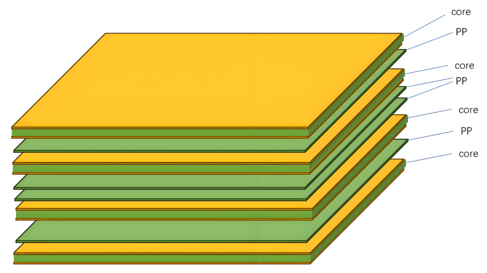
Designing a reliable multilayer circuit board starts with getting the stackup right. If your project involves high-speed signals, compact layouts, or reduced EMI, an 8-layer PCB stackup is a solid choice. It offers flexibility, better performance, and room for complex routing.
In this guide, we’ll walk you through everything you need to know—layer configurations, materials, sizes, and how to make the most of this structure with the help of a trusted PCB manufacturer.
What is a PCB Stackup?
A PCB stackup is the arrangement of copper layers and insulating materials inside a circuit board. These layers are stacked and bonded together using prepreg (resin-impregnated fiberglass) and core materials. The goal is to create a reliable board that supports both mechanical strength and excellent electrical performance.
In simple words, the stackup decides how signal layers, power planes, and ground layers are placed in the board. In high-speed digital designs, this structure plays a big role in signal quality, electromagnetic compatibility (EMC), and overall performance.
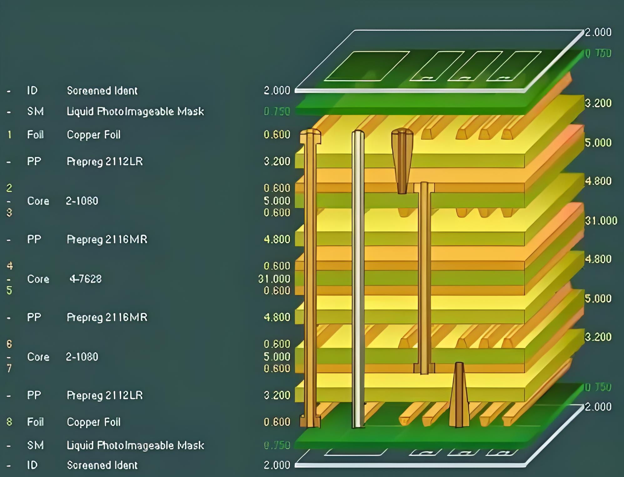
For an 8-layer PCB, the stackup consists of eight layers of copper with alternating dielectric materials. These are usually divided into four signal layers and four plane layers, though that can change based on your design needs.
PCB Stackup Considerations
For most PCB designs, there are often competing requirements between electrical performance, manufacturing limitations, cost targets, and system complexity. The final PCB stackup is usually a result of careful trade-offs across these factors. High-speed digital circuits and RF systems commonly rely on multilayer boards for better control and performance. Below are 8 essential principles to consider when designing a reliable stackup:
1. Layer Arrangement
In multilayer PCBs, you’ll typically work with signal layers (S), power planes (P), and ground planes (GND). Power and ground planes are usually solid, unbroken areas that provide low-impedance return paths for signal currents. Signal layers are often positioned between these planes to form symmetrical or asymmetrical stripline structures. The top and bottom layers are mainly used for component placement and limited routing. It’s best to keep traces on these outer layers short to reduce direct radiation and EMI.
2. Defining a Single Power Reference Plane
Decoupling capacitors are vital for maintaining power integrity, and they can only be placed on the outer layers of the PCB. The trace length, pad design, and vias connected to these capacitors greatly affect their effectiveness. To improve decoupling, make these connections short and wide, and minimize via length. For example, in a high-speed digital system, place decoupling capacitors on the top layer, dedicate the second layer to power for the processor, use the third layer for signal routing, and assign the fourth layer as a ground reference.
3. Incorporating Multiple Ground Planes
Using multiple ground planes helps create low-impedance return paths and minimizes common-mode EMI. Ground and power planes should be tightly coupled, and signal layers should also be close to reference planes. Reducing the dielectric thickness between layers improves coupling and enhances performance.
4. Managing Multiple Power Planes
When your design includes more than one power plane, these planes are often split into different voltage regions. If a signal layer is placed next to a multi-region power layer, signal currents may not find clean return paths, leading to noise or EMC issues. For high-speed digital signals, avoid routing traces near split power planes to prevent return current discontinuities.
5. Designing Signal Routing Pairs
When a signal travels from one layer to another, it creates what’s known as a “routing pair.” Ideally, the return current should stay within the same reference plane when switching layers. In practice, however, signals often need to transition between layers. To maintain signal integrity, ensure that return paths are available through stitching vias or decoupling capacitors. Using adjacent layers as routing pairs is a practical and effective strategy.
6. Routing Direction Guidelines
Keep trace directions consistent within each signal layer. At the same time, rotate the routing direction between adjacent signal layers. For instance, use horizontal routing (X-axis) on one layer and vertical routing (Y-axis) on the next. This practice reduces crosstalk and improves signal clarity.
7. Even-Layer Designs is Better
Although odd-layer PCBs may appear cheaper due to fewer materials, they’re more expensive to manufacture. That’s because odd-layer boards require non-standard lamination processes and additional handling steps. These increase the risk of surface damage, incorrect etching, and longer production times. In contrast, even-layer PCBs are more stable, cost-effective, and easier to produce at scale.
8. Budget
Multilayer PCBs are naturally more expensive than single- or double-layer boards. However, they offer significant benefits in functionality, miniaturization, EMI control, and signal integrity. When weighing total cost versus performance, the difference between multilayer and simpler boards may not be as high as expected.
Standard 8-Layer PCB Stackup Structure
When it comes to multilayer PCB design, the arrangement of signal, power, and ground layers directly affects signal integrity, EMI performance, and power delivery. Below are three common 8-layer stackup configurations, each with its own strengths and limitations.
Option 1:
Layer 1: Signal 1
Layer 2: Signal 2
Layer 3: Ground
Layer 4: Signal 3
Layer 5: Signal 4
Layer 6: Power
Layer 7: Signal 5
Layer 8: Signal 6
This layout alternates signal and power layers but does not take full advantage of the electromagnetic shielding benefits that a multilayer board can offer. The ground and power planes are separated, reducing the board’s EMI suppression capability. In addition, the power distribution network suffers from higher impedance, which may affect voltage stability in high-speed or high-current applications.
Option 2:
Layer 1: Signal 1
Layer 2: Ground
Layer 3: Signal 2
Layer 4: Power
Layer 5: Ground
Layer 6: Signal 3
Layer 7: Ground
Layer 8: Signal 4
This structure is widely regarded as the optimal 8-layer PCB stackup. It provides excellent electromagnetic shielding through the use of multiple ground planes. Each signal layer is placed adjacent to a reference plane (either ground or power), which improves signal stability and impedance control. Additionally, the tight coupling between power and ground planes enhances EMI performance and power integrity. This setup is ideal for high-speed, high-frequency, or noise-sensitive applications.
Option 3:
Layer 1: Signal 1
Layer 2: Ground
Layer 3: Signal 2
Layer 4: Power
Layer 5: Ground
Layer 6: Signal 3
Layer 7: Power
Layer 8: Signal 4
This configuration is a variation of Option 1 with improved EMI performance. By adding an extra reference plane, it provides better control over the characteristic impedance of the signal layers. However, the placement of the second power plane (with limited coupling to a nearby ground) leads to higher power delivery impedance, which could be a drawback in power-sensitive designs. Some optimization in power layer arrangement is still needed.
8-Layer PCB Stackup Materials
The performance of an 8-layer PCB stackup relies heavily on the materials used between and around its copper layers. These materials affect everything from electrical behavior to thermal stability and even mechanical strength. Let’s look at the two main categories: conductive and dielectric materials.
1. Conductive Layers
Copper is the most common metal used for the conductive layers in an 8-layer PCB. It’s highly conductive, easy to work with, and available in different thicknesses and finishes.
Copper Thickness: Most boards use ½ oz or 1 oz copper per layer. If the design needs to handle higher current, 2 oz or thicker copper may be used.
Copper Type: Standard copper foil is either electrodeposited (ED) or rolled. Rolled and annealed copper is smoother and more flexible, which makes it useful in boards that need better bend resistance.
Surface Finishes: The exposed copper is usually treated with a surface finish to protect it and ensure solderability. Options include HASL, ENIG, OSP, and immersion silver, among others.
2. Dielectric Layers
The dielectric materials are the insulating layers that separate the copper traces. These layers are critical for controlling impedance, heat flow, and electrical isolation.
FR-4: A glass-reinforced epoxy laminate, FR-4 is the most common dielectric for general-purpose PCBs. It’s reliable, widely available, and cost-effective.
High-Frequency Materials: For RF and high-speed digital designs, materials with low dielectric loss—like PTFE (Teflon), ceramic-filled PTFE, or hydrocarbon-based ceramics—are preferred. These support better signal integrity at high frequencies.
Thermal Conductive Materials: When heat dissipation is a concern, substrates like alumina or aluminum nitride are used. These materials offer higher thermal conductivity than standard epoxy systems.
To hold everything together, manufacturers use prepregs—uncured fiberglass sheets soaked in resin. Common prepreg materials include FR-4 for standard designs and polyimide for higher thermal or mechanical stress environments.
At the center of the stackup is the core, which acts like a spine for the board. This rigid layer typically uses FR-4 or polyimide, though in some high-power or high-heat applications, metal cores are added to improve thermal performance.
8-Layer PCB Thickness & Sizes
The total thickness of an 8-layer PCB depends on several factors:
Copper thickness: Common values are 0.5oz, 1oz, or 2oz per layer.
Prepreg/Core thickness: Adjusted to achieve specific impedance and board height.
Number of plane vs signal layers: Affects thermal and mechanical behavior.
Common Thickness Options:
1.6mm (0.063″) – Industry standard, suitable for most applications.
2.0mm to 2.4mm – Used when extra copper is needed for higher current.
3.2mm or custom – Selected for industrial or military-grade boards.
PCB Sizes:
Panel sizes are typically 18” x 24” before routing. Your board can be as small as a few millimeters or as large as the full panel, depending on the application.
6 Layer vs 8 Layer PCB
A 6-layer PCB consists of six layers of copper circuitry stacked with insulating layers (prepreg and core) in between. It usually includes:
4 Signal Layers for routing high- and low-speed signals
1 Power Plane to distribute voltage
1 Ground Plane to provide a return path and help with EMI suppression
A typical 6-layer stackup looks like this:
Layer 1: Signal (Top)
Layer 2: Ground
Layer 3: Signal
Layer 4: Signal
Layer 5: Power
Layer 6: Signal (Bottom)
While both 6-layer and 8-layer PCBs are widely used in advanced electronics, they serve slightly different purposes depending on design complexity, signal speed, and EMI requirements. Let’s compare them together:
Aspect
6-Layer PCB
8-Layer PCB
Layer Count
6
8
Typical Configuration
4 signal layers + 1 power + 1 ground
4 signal layers + 2 power + 2 ground
Routing Space
Moderate
More routing room
Signal Integrity
Good, suitable for most mid-speed signals
Excellent, supports very high-speed signal routing
EMI Shielding
Limited shielding with fewer ground planes
Strong EMI control due to multiple ground planes
Power Distribution
Single power plane, higher impedance
Dual power planes, better PDN performance
Design Complexity
Less complex, easier to design and fabricate
More complex, better for advanced designs
Thermal Performance
Adequate for medium power applications
Better heat spreading for high-power components
Cost
Lower fabrication cost
Higher cost due to more layers and materials
Use Case
Mid-level MCUs, general embedded, basic RF
FPGAs, DDR memory, high-speed data buses, complex SoCs
Use a 6-Layer PCB if:
Your design isn’t extremely dense.
The signals don’t require tight EMI control.
You want to balance performance and cost.
There’s no strict need for multiple ground or power planes.
It’s widely used in commercial electronics that don’t involve ultra-high-speed communication or compact multilayer routing challenges.
Choose an 8-Layer PCB when:
High-speed signals (such as PCIe, USB 3.x, DDR4, or SERDES) are involved.
EMI performance is critical, especially in sensitive industrial or medical devices.
You need more space for routing due to a denser component layout.
Stable power delivery is required across multiple voltage domains.
You’re working with a compact form factor that demands vertical signal distribution.
An 8-layer stackup allows designers to pair every signal layer with a nearby ground or power plane, which significantly improves signal quality and reduces noise.
Benefits of Working with an Experienced PCB Manufacturer
Designing and fabricating an 8-layer PCB stackup requires precise engineering and process control. Partnering with a reliable manufacturer like EBest Circuit (Best Technology) brings several benefits:
1. Stackup Design Assistance: Professional help with impedance control, signal integrity, and EMC optimization.
2. Material Expertise: Guidance in choosing suitable laminates for your specific requirements.
3. Advanced Fabrication: Capability to handle HDI, blind/buried vias, and tight tolerances.
4. Quality Assurance: Rigorous testing like AOI, X-ray, and impedance measurement.
5. Fast Turnaround: Efficient production process without sacrificing quality.
Why Choose EBest Circuit (Best Technology) for Your 8-Layer PCB Stackup?
EBest Circuit (Best Technology) is a trusted 8-layer PCB stackup specialist serving global customers across aerospace, medical, automotive, and industrial electronics. We hold certifications including:
ISO9001 for quality control
ISO13485 for medical electronics
IATF16949 for automotive-grade PCBs
AS9100D for aerospace applications
Our engineers assist with DFM check, impedance control, EMI reduction, thermal management, and material choices, ensuring your 8-layer design performs reliably under real-world conditions.
FAQs
1. What is the best layer configuration for an 8-layer PCB stackup?
A balanced configuration like Signal–GND–Signal–Power–GND–Signal–Power–Signal is often preferred for signal integrity and EMI control.
2. How much does an 8-layer PCB cost?
Cost varies by material, size, copper weight, and complexity, but typically ranges from $50 to $300 per board in small batches.
3. What software is used for 8-layer PCB design?
Tools like Altium Designer, Eagle, KiCAD, and OrCAD support multilayer PCB stackup planning and layout.
4. Can you use HDI features in 8-layer PCBs?
Yes. Blind and buried vias, via-in-pad, and microvias are often used in 8-layer HDI designs.
5. How do I choose the right manufacturer for 8-layer PCBs?
Look for certifications, material options, engineering support, and experience with multilayer stackups—like what EBest Circuit (Best Technology) provides.
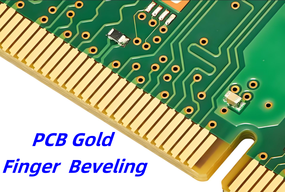
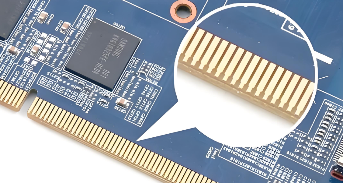
Gold fingers are one of the most critical features in many circuit boards, especially those used in high-reliability connections. Whether you’re building a test interface, designing a PCIe card, or creating an edge connector, understanding gold finger beveling and its plating design is essential for durability and smooth performance.
Let’s explore everything about PCB gold fingers, the beveling process, and how to choose the right beveling angle for your board design.
What Is a Gold Finger?
PCB gold fingers are the gold-plated connectors located along the edge of a printed circuit board. They serve as contact points when a PCB is inserted into a slot or connector, just like in RAM, GPU cards, or other modular systems. These fingers are plated with hard gold to ensure they can withstand repeated insertion and removal cycles without wearing out.
They are called “fingers” because they look like narrow, elongated pads stretching along the PCB’s edge, similar to the fingers of a hand. Each gold finger connects to a circuit trace inside the board. When the PCB is inserted into a slot, the metal contacts on the gold fingers align with the contacts inside the connector, allowing signals to pass through.
The main reason gold is used is because it doesn’t corrode easily. Gold provides high conductivity and can withstand many insertions without losing its shape or functionality. In critical environments—like military, aerospace, or telecom—this reliability is essential.
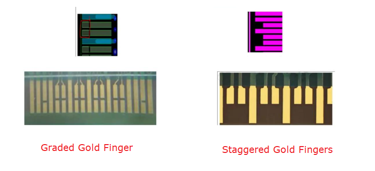
Types of Gold Fingers in PCB
PCB gold fingers can be divided into two types – graded gold fingers and staggered gold fingers.
Graded Gold Finger
Graded gold fingers refer to a design where the fingers are plated with gold at varying lengths or staggered elevations. Instead of all the fingers being aligned in a straight line, some are slightly longer than others. This is not just a visual variation—it serves a very specific purpose. Graded fingers are typically used in applications where controlled insertion sequencing is required. When the PCB is inserted into the slot, the longer fingers make contact first, followed by the shorter ones.
Staggered Gold Fingers
Another design strategy is using long and short gold fingers—also known as staggered gold fingers. This refers to gold fingers of different physical lengths on the same board edge, but typically without beveling or plating depth variation. This technique is commonly used in:
PCIe hot-pluggable cards
Industrial control systems with replaceable modules
Burn-in or test fixtures requiring safe first-contact
The lengths are designed based on the depth of the connector slot and how the PCB enters the socket. Sometimes only a few pins—such as GND or VCC—are made longer, while the rest remain short.
How Thick Is PCB Gold Finger Plating?
The durability of gold fingers comes from their plating thickness. Not all gold fingers are created equal. The thickness of the plating affects both how well they perform and how long they last.
The gold layer is not pure; it is electroplated hard gold, which includes a bit of cobalt to improve hardness and wear resistance. Here’s a breakdown of common thicknesses:
Application Type
Gold Plating Thickness (Hard Gold)
Standard Consumer Devices
0.76μm (30μin)
Industrial or Light Insertion
1.27μm (50μin)
High-Durability Applications
2.54μm (100μin)
In general, 50μin is the most common for boards that are plugged and unplugged many times. If the fingers are not meant to be removed often, thinner plating is usually fine. But when in doubt, thicker is better—it provides stronger wear resistance.
What Is the Process of Gold Plating in PCB?
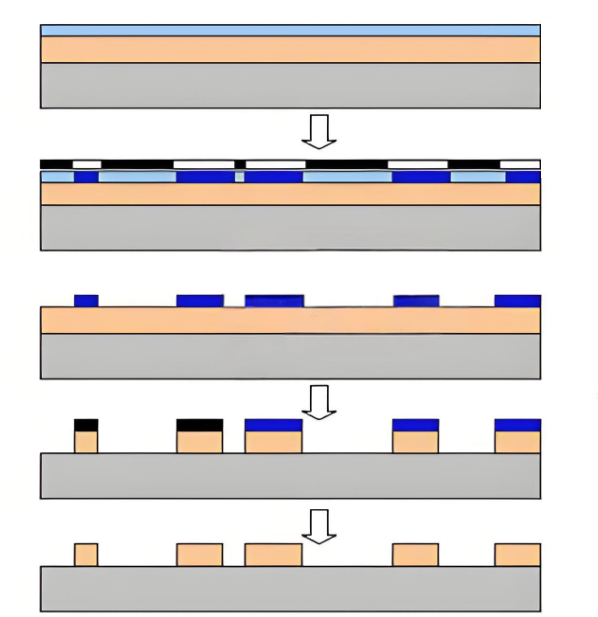
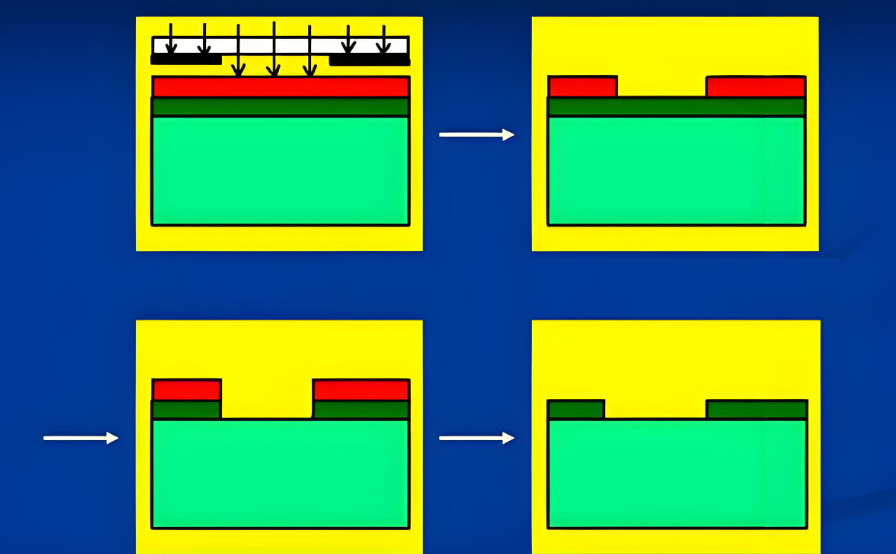
Creating strong, reliable pcb gold fingers requires precision. The plating process is done after the rest of the board is fabricated and cleaned. The focus is to add a hard gold layer only to the fingers—nowhere else. Here’s how the PCB gold finger plating process works step-by-step:
1. Finger Area Isolation
First, the PCB is cleaned, and only the finger areas are exposed. The rest of the board is masked to prevent unwanted plating elsewhere.
2. Nickel Plating (Bottom layer)
A nickel layer (typically 3–6μm) is electroplated onto the copper finger base. Nickel improves gold adhesion and acts as a barrier to prevent copper from diffusing into the gold over time.
3. Gold Electroplating (Top Layer)
After nickel, a layer of hard gold is plated on top. This layer is usually between 30μin and 100μin depending on the application. The plating uses a current that drives gold ions onto the nickel surface.
4. Cleaning and Inspection
Once the plating is complete, the board is cleaned, and the gold fingers are inspected for uniformity, roughness, or any missing areas.
5. Beveling (If Required)
If beveling is needed, it is done after plating. The edge is shaped to allow easier insertion into connectors.
6. Final Finishing
The rest of the PCB receives its finish (e.g., ENIG, OSP, HASL), but gold fingers remain untouched.
This plating method results in durable, smooth connectors that resist oxidation and mechanical wear.
What Is Gold Finger Beveling?
Gold finger beveling is a mechanical process that trims the edge of the PCB—where the gold fingers are located—into a sloped angle. Rather than a blunt 90° edge, the bevel creates a smooth ramp-like surface.
Imagine sliding a PCB into a connector. A sharp edge might catch, damage the connector, or scrape off the plating. But a beveled edge slides in smoothly, reducing friction and improving contact.
This is especially useful for PCBs used in:
Backplane systems
Server racks
Communication modules
Plug-and-play components
The beveling process is typically done using precision grinding or CNC milling. Care is taken to maintain exact angle measurements without overcutting the gold plating.
Purpose of Gold Finger Beveling
There are several important reasons why beveling is applied to PCB gold fingers:
Easier Insertion
A beveled edge helps the PCB slide into the connector smoothly. It reduces the chance of misalignment or jamming.
Prevents Contact Damage
Without beveling, the sharp PCB edge can scratch the connector pins, causing early wear or performance issues.
Reduces Wear and Tear
Repeated insertion cycles can wear out the gold plating. Beveling distributes the pressure more evenly, extending the lifespan of both board and connector.
Better Electrical Contact
Smoother insertion means better alignment and tighter contact with the metal pins inside the slot. This leads to more stable signals and fewer connection errors.
Professional Manufacturing Finish
Beveled gold fingers look more refined, signaling high-quality PCB craftsmanship.
For any board that’s going to be removed and reinserted frequently, beveling is not just a good idea—it’s almost essential.
Gold Finger Beveling Angle Options
When beveling, you have options for the bevel angle. The choice depends on how the PCB fits into its slot and the degree of insertion force you want to reduce. Here are the common beveling angles:
Angle
Description
30°
The most popular angle. Balances mechanical strength and ease of insertion.
40°
Offers a smoother slope than 30°. Used when insertion needs to be gentle.
45°
The steepest slope. Useful when the board must glide into the slot with minimal resistance.
Most applications stick with 30°, but you should always check the connector specification. Some high-density or high-speed connectors might require tighter tolerances and smoother entry paths.
Considerations of Beveling Angles
Before you finalize your beveling angle, consider the following:
Slot Geometry
Look at how your connector or socket is shaped. If the slot opening is narrow, a steeper bevel (like 45°) might be helpful.
Insertion Frequency
If the PCB will be removed often—like in test or modular setups—a smoother entry reduces long-term damage.
Mechanical Strength
Sharper bevels remove more material. If your board edge carries mechanical load, avoid overly steep bevels.
Gold Coverage
The beveling process should never cut through the gold. Make sure the gold plating thickness is enough to cover the entire bevel.
IPC Guidelines
Refer to IPC-6012 and IPC-A-600 for guidelines on gold finger design, plating, and beveling requirements.
Always coordinate with your PCB manufacturer to ensure the chosen bevel angle is feasible and matches your product’s functional needs.
PCB Gold Fingers Applications
Gold fingers are everywhere. Any device that uses edge connectors likely has them. Some of the most common use cases include:
Graphics cards (GPU) – for connecting with the motherboard
RAM modules – inserted into DIMM slots
Motherboards and backplanes – for communication between layers or devices
Test interface boards – for burn-in, programming, or debugging
PLC and industrial control systems – for module plug-in
Medical and defense electronics – where reliability is critical
In all these applications, gold finger beveling helps ensure the boards don’t fail during connection or removal. It may seem like a small detail, but its effect on reliability is huge. Gold finger beveling is one of those small but powerful features that improves the mechanical fit, electrical contact, and overall durability of your circuit boards. When designing your next PCB, pay attention to:
The gold finger plating thickness
Whether beveling is needed
The best angle for smooth insertion
And the wear-and-tear the board will experience
These decisions affect not only how well the board works, but how long it lasts.
About EBest Circuit (Best Technology)
At EBest Circuit (Best Technology), we specialize in PCB manufacturing with a focus on high-reliability boards. We handle everything from custom hard gold finger design to precision beveling, ensuring your edge connectors meet international standards. Our team works with industries including medical, automotive, aerospace, and telecom.
We follow strict quality processes and use MES traceability systems to track every step. Whether you need quick prototypes or high-volume production, our engineers are ready to help you design, test, and deliver high-performance PCBs with durable gold fingers.
Looking for a PCB manufacturer that understands the details? Let’s build your next project together.
FAQs
1. Can I design gold fingers without beveling?
Yes, but for any board that will be plugged in and out regularly, beveling is highly recommended for smoother insertion and longer lifespan.
2. What’s the difference between ENIG and hard gold?
ENIG is used on pads for soldering. Hard gold is plated on fingers for wear resistance. They are different in composition and use.
3. How do I specify beveling on my Gerber files?
You should include a separate mechanical drawing or notation in the fabrication notes to indicate the beveling angle and location.
4. Are gold fingers more expensive to produce?
Yes, due to the electroplating process and gold material cost. However, they add significant durability and value.
5. Can gold finger plating wear off?
Over time, yes—especially if the plating is thin. Using thicker plating like 50μin or more helps prevent this.
Rogers RO4350B is one of the most popular PCB materials used in high-frequency applications today. If you’re designing circuits that need stable performance at GHz-level speeds, this material often stands out. In this blog, we’ll explore what RO4350B is, what it’s made of, available thicknesses, and why it’s preferred over other materials for high-frequency PCB designs.
What Is Rogers RO4350B Material?
RO4350B is a type of high-frequency laminate developed by Rogers Corporation. It’s engineered for performance in RF (radio frequency) and microwave applications, offering superior electrical characteristics compared to standard FR-4. Unlike generic epoxy-based materials, RO4350B uses a hydrocarbon-ceramic composition that keeps signal losses low even at high frequencies.
This material combines the electrical performance of PTFE (commonly used in high-end RF applications) with the manufacturability of FR-4, making it a cost-effective and reliable choice for high-speed designs.
What Is Rogers Material Made of?
Rogers materials, including RO4350B, are made from hydrocarbon resins with ceramic fillers and reinforced with woven glass. This composite structure delivers excellent mechanical stability and consistent dielectric properties.
Unlike traditional PTFE-based laminates, Rogers materials like RO4350B do not require special handling during PCB fabrication, which saves both time and cost. Rogers materials are engineered to balance electrical performance with ease of manufacturing, which is essential when producing high-frequency PCBs at scale.
RO4350B Dielectric Constant
The dielectric constant (Dk) is a critical factor in high-frequency PCB materials, as it affects signal speed and impedance control. The RO4350B dielectric constant is typically 3.48 ± 0.05 at 10GHz, which is both stable and predictable over a wide range of frequencies and temperatures.
The consistency of frequencies and temperatures ensure that transmission lines behave as expected, which is especially important in RF circuits, microwave devices, and antenna structures. Stable Dk also simplifies impedance control and reduces the risk of signal reflection and distortion.
What Is the Standard RO4350B Thickness?
RO4350B PCBs are available in multiple standard thicknesses to meet different design and performance requirements. Common options include:
0.254 mm (10 mil)
0.508 mm (20 mil)
0.762 mm (30 mil)
1.524 mm (60 mil)
These thicknesses allow designers to select the best stack-up for impedance control, thermal dissipation, and mechanical strength. Depending on your signal layer, ground layer spacing, or copper weight, one of these thicknesses will likely align with your project’s needs.
RO4350B Datasheet
Before choosing a material for your RF or high-speed digital PCB, it’s essential to understand the technical specifications. Here is a summary of the most important values from the RO4350B datasheet:
Property
Typical Value
Test Condition / Note
Dielectric Constant (Dk)
3.48 ± 0.05
@ 10 GHz (z-axis)
Dissipation Factor (Df)
0.0037
@ 10 GHz
Volume Resistivity
1.7 × 10⁸ MΩ·cm
ASTM D257
Surface Resistivity
4.4 × 10⁷ MΩ
ASTM D257
Electrical Strength
>800 V/mil
ASTM D149
Dielectric Breakdown
>40 kV
ASTM D149
Thermal Conductivity
0.69 W/m·K
ASTM D5470
Coefficient of Thermal Expansion (CTE)
11 ppm/°C (x, y) / 32 ppm/°C (z)
-55°C to 288°C
Glass Transition Temperature (Tg)
>280°C (no defined Tg)
Thermomechanical analysis
Decomposition Temperature (Td)
~425°C
TGA method
Solder Reflow Resistance
Excellent
No delamination or blistering
Tensile Modulus
1.4 × 10⁶ psi (x-y)
ASTM D638
Flexural Strength
20,000 psi (typical)
ASTM D790
Peel Strength
≥1.1 N/mm
IPC-TM-650
Young’s Modulus
~10 GPa
Estimated from stress-strain curve
Moisture Absorption
0.06%
ASTM D570
Density
1.86 g/cm³
ASTM D792
Flammability Rating
UL 94 V-0
UL 94
Water Absorption
<0.1%
Excellent water resistance
Material Composition
Ceramic-filled hydrocarbon resin + glass fiber
Non-PTFE-based
Halogen-Free
Yes
RoHS & REACH compliant
Available Copper Foil
0.5 oz, 1 oz, 2 oz (18µm, 35µm, 70µm)
Rolled and electro-deposited options available
If you need the full official datasheet in PDF format, you can also request it from EBest Circuit (Best Technology) along with a quote for your project.
How Much Does Rogers PCB Cost?
Compared to FR-4, the rogers RO4350B price is higher due to its premium performance. On average, RO4350B material can cost between $8 to $25 per square foot, depending on thickness, copper weight, and supplier volume. Full PCB fabrication using RO4350B typically results in a 20–50% higher price than using standard FR-4, mainly due to the material cost and additional processing steps.
However, when you’re working with high-frequency applications—such as 5G, radar, or satellite communications—the improved signal integrity and reduced loss often justify the added cost.
What Is the Difference Between RO4003 and RO4350B?
Both RO4003 and RO4350B are part of Rogers’ high-frequency laminate series, but they have subtle differences:
Feature
RO4003C
RO4350B
Dielectric Constant
3.38
3.48
Loss Tangent
0.0027 @ 10 GHz
0.0037 @ 10 GHz
Flame Rating
Non-UL rated
UL 94 V-0
Cost
Slightly lower
Slightly higher
Process Compatibility
Standard PCB process
Standard PCB process
RO4003 is better suited for applications where cost sensitivity is critical and UL rating is not required. RO4350B, on the other hand, provides a better flame rating and slightly improved mechanical properties, so it is the preferred choice for commercial or defense-grade applications.
Why Choose RO4350B as High Frequency PCB Material?
High frequency PCB, also known as RF PCB, refers to a special circuit boards with relatively high electromagnetic frequencies. This PCB is mainly used in the fields of high frequency (>300 MHz or wavelengths <=1 meter) and microwaves (>3 GHz or wavelengths <= 0.1 meter). If you’re designing a high-frequency PCB, choosing RO4350B gives you the best of both worlds: high performance and ease of fabrication. Here’s why many engineers choose this material:
Low dielectric loss helps reduce signal attenuation.
UL 94 V-0 flame resistance, which is crucial for safety.
Compatible with standard FR-4 processing, so no need for Teflon-specific tooling.
All of these feature help maintain signal quality in applications like RF transmitters, satellite receivers, and high-speed digital circuits. So even if the RO4350B price is slightly higher, it’s often more cost-effective than debugging performance issues caused by suboptimal materials.
High Frequency PCB Design Guidelines
When working with RO4350B PCB material, keep the following design practices in mind to get the best results:
1. Control impedance: Use proper stack-up and trace width calculators for accurate 50Ω or 75Ω routing.
2. Minimize vias: Each via introduces inductance and can distort signals at high frequencies.
3. Short trace lengths: High-speed signals should have the shortest possible paths.
4. Proper grounding: Always include a continuous ground plane to reduce EMI and improve return paths.
5. Avoid sharp corners: Use 45-degree or curved traces instead of 90-degree angles.
6. Use differential pairs: For high-speed interfaces like USB or LVDS, tightly coupled pairs reduce crosstalk and maintain signal integrity.
Combining these techniques with the natural performance of RO4350B helps you unlock superior RF performance without increasing fabrication complexity.
Why EBest Circuit (Best Technology) Is Your Reliable RF PCB Manufacturer?
At EBest Circuit (Best Technology), we specialize in high-frequency PCB manufacturing using premium materials like RO4350B, RO5880, RO4003C. With ISO-certifications, we’re equipped to serve industries ranging from automotive and medical to aerospace and communications. Whether you’re developing high-reliability prototypes or large-scale production, you can count on us as your reliable one-stop PCB & PCBA partner.
We offer:
Strict impedance control with advanced test equipment
Rapid prototyping and flexible volume production
Competitive RO4350B price with guaranteed traceability
Expert engineering support for layout and material selection
No MOQ requires, 1 piece available also
5 years quality guarantee, free rework and functional testing
Free DFM check
If you’re looking to manufacture reliable high-frequency PCBs, you’re in the right place.
FAQs
1. Is RO4350B suitable for multilayer PCBs?
Yes, RO4350B is commonly used in multilayer designs for RF and microwave applications. It offers stable performance in both single and multi-layer stack-ups.
2. How does RO4350B perform at 5GHz or higher?
It maintains low loss and consistent Dk values even at frequencies above 5GHz, making it reliable for 5G and radar circuits.
3. Can RO4350B be used with FR-4 in hybrid stack-ups?
Yes, it can. Many engineers use RO4350B for RF layers and FR-4 for power/control layers to reduce cost.
4. What is the shelf life of RO4350B material?
Stored under proper conditions, it has a long shelf life—typically over a year without degradation.
5. Do I need special PCB fabrication for RO4350B?
No. Unlike PTFE-based materials, RO4350B is compatible with standard PCB fabrication processes, which simplifies manufacturing.
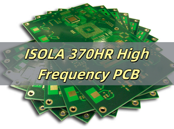
Isola 370HR is a well-established choice for engineers who need a durable, high-frequency compatible PCB base material. Its high Tg, low loss, and excellent reliability make it suitable for everything from aerospace to telecommunications.
If you’re working on a complex design or RF application, switching to Isola 370HR PCB materials might be the upgrade you need. And with a reliable partner like EBest Circuit (Best Technology), you’re assured of quality from the first prototype to volume production.
What Is Isola 370HR Material?
Isola 370HR is a high-performance, high-Tg epoxy laminate and prepreg system developed by Isola Group. Designed specifically for multilayer printed circuit boards, it offers a great balance between electrical stability and thermal durability. It’s classified as a high-Tg FR4 material but provides better signal handling and thermal behavior compared to standard FR4.
Isola engineered this material for demanding sectors like telecommunications, data networking, and military electronics. Its low dielectric loss and stable performance across a wide frequency range make it suitable for modern high-speed circuits.
Advantages of Using Isola 370HR in PCB Manufacturing
Choosing Isola 370HR for your PCB manufacturing brings several key benefits that directly impact the performance and reliability of your finished products:
Superior Thermal Stability: With a high glass transition temperature (~180°C), Isola 370HR withstands the high temperatures of lead-free soldering and multiple reflow cycles without warping or delamination.
Low Dielectric Loss: This material minimizes signal loss at high frequencies, making it perfect for RF circuits and high-speed digital designs.
Excellent Signal Integrity: Stable dielectric constant (Dk) across frequency ranges means consistent signal propagation and reduced timing errors.
Enhanced Moisture and CAF Resistance: Improved resistance to moisture-induced failures helps maintain long-term reliability, especially in humid or harsh environments.
Dimensional Stability: Reduced Z-axis expansion ensures layers stay aligned during manufacturing and operation, critical for multilayer PCBs.
IPC Compliance: Isola 370HR meets rigorous industry standards, ensuring compatibility with demanding aerospace, automotive, and medical applications.
RoHS and Environmental Compliance: Fully compliant with environmental regulations, supporting green manufacturing practices.
ISOLA 370HR Datasheet
Property
Typical Value
Test Method / Notes
Glass Transition Temperature (Tg)
180°C (DSC)
Differential Scanning Calorimetry
Decomposition Temperature (Td)
>340°C
TGA (Thermogravimetric Analysis)
Dielectric Constant (Dk)
4.04 @ 1 GHz
IPC-TM-650 2.5.5.5
Dissipation Factor (Df)
0.0127 @ 1 GHz
IPC-TM-650 2.5.5.5
Coefficient of Thermal Expansion (CTE)
15 ppm/°C (X-Y), 65 ppm/°C (Z)
IPC-TM-650 2.4.24
Thermal Conductivity
0.4 W/m·K
ASTM E1461
Tensile Strength
24,000 psi
IPC-TM-650 2.4.18
Flexural Strength
32,000 psi
IPC-TM-650 2.4.4
Water Absorption
<0.10%
IPC-TM-650 2.6.2.1
Flammability Rating
UL 94 V-0
UL 94
Copper Peel Strength
>1.0 lbs/inch
IPC-TM-650 2.4.8
Surface Resistivity
>1×10^6 ohms
ASTM D257
Volume Resistivity
>1×10^9 ohm-cm
ASTM D257
Dielectric Breakdown Voltage
>50 kV/mm
IPC-TM-650 2.5.6
What Is the Difference Between FR4 and 370HR?
While both standard FR4 and Isola 370HR are epoxy-based materials widely used in PCB manufacturing, they differ significantly in performance—especially when it comes to high-speed and high-frequency applications.
Standard FR4 is the go-to material for many general-purpose PCBs. It offers decent mechanical strength, good manufacturability, and cost-effectiveness for everyday electronics. However, its glass transition temperature (Tg) typically ranges from 130°C to 140°C, and it has relatively higher dielectric loss (Df). These limitations can cause signal degradation and reliability issues in circuits operating at higher frequencies or elevated temperatures.
In contrast, Isola 370HR is a high-Tg FR4 variant designed to meet the demands of more challenging environments. Its Tg is around 180°C, which provides superior thermal stability during lead-free soldering and extended use in high-temperature settings. More importantly, it exhibits a lower dielectric constant (Dk) and dissipation factor (Df), which translates to lower signal loss and better signal integrity at microwave and radio frequencies.
Why Isola 370HR PCBs Are Suitable for High Frequency Applications?
As electronic devices evolve to support faster data rates, the performance of PCB materials under high-frequency conditions has become a serious concern. This is where Isola 370HR PCB materials shine.
Its consistent dielectric constant (Dk) and low dissipation factor (Df) ensure that high-frequency signals do not lose strength or become distorted. That’s a major reason why 370HR is used in:
Gigabit Ethernet systems
High-speed backplanes
Automotive radar systems
Satellite communications
Advanced test equipment
Its ability to handle GHz-level signals without distortion helps maintain data accuracy and reduces EMI-related issues.
When to Choose Isola 370HR Material for Your PCB?
You might consider Isola 370HR when your design falls into any of the following categories:
High-speed or RF designs: If your circuit runs at over 1 GHz, this material can preserve signal quality.
Multilayer PCBs: When stacking 8 or more layers, 370HR offers great registration control and stability.
Thermal stress tolerance: It performs reliably through multiple reflow cycles and temperature extremes.
CAF-resistant needs: Ideal for products exposed to moisture or long-term outdoor use.
Strict industry compliance: It meets IPC-4101/126 and 129, as well as UL and RoHS requirements.
Choosing this material isn’t just about performance—it’s about peace of mind over the product’s lifecycle.
How to Identify Genuine Isola 370HR PCB Material?
To avoid counterfeit materials or unverified substitutions, it’s important to:
Request the original datasheet with the Isola logo and batch number.
Check board markings for Isola brand identification or laminate codes.
Work with certified suppliers who purchase directly from Isola or its authorized distributors.
Ask for certification documents, especially if your application is regulated by aerospace or medical standards.
Genuine Isola 370HR PCB materials ensure consistency in production and performance.
Typical Applications of Isola 370HR in PCB Design
Here are common industries and devices where Isola 370HR is frequently used:
Telecommunications: High-speed switches, routers, and fiber optic systems.
Aerospace and Defense: Radar, avionics, satellite boards.
Medical Equipment: Imaging devices, patient monitoring systems.
Automotive: Advanced driver-assistance systems (ADAS), LiDAR modules.
Industrial Automation: Motor controls, power management systems.
Designers across these sectors rely on its thermal reliability and signal control to reduce field failures.
What Is the Equivalent of Isola 370HR?
While Isola 370HR is a preferred material, there are other options that offer similar characteristics. Here’s how some alternatives compare:
Material Name
Tg (°C)
Df @ 1GHz
Notable Feature
Nelco N4000-13EP
~180
~0.013
Known for stability
Panasonic MEGTRON 6
~185
~0.0025
Ultra-low loss, but expensive
Ventec VT-47
~180
~0.014
Cost-effective option
If you need better electrical performance than 370HR, MEGTRON 6 is a great choice. For general high-frequency use with cost control, 370HR remains the most balanced option.
With over 18 years of experience in printed circuit boards and as one of the leading PCB manufacturers, we support over 1,000 customers in different industrial areas worldwide. You can count on a PCB board manufacturer like us to meet your one-stop electronics manufacturing demands.
We are your one-stop PCB manufacturer in China who can meet all your diversified PCB requirements. We have an experienced engineering, production, and quality team that fully understands the unique needs of your industry—especially in medical, automotive, and aerospace applications. As a printed circuit board manufacturer, we always follow the most widely accepted standards in the industry: IPC-A-600 for fabrication and IPC-A-610 for PCB assembly. All our products meet IPC Class 2 by default, and we can also meet Class 3 or 3A when your application requires it.
If you have any questions about our products, services, pricing, lead times, quality control, certifications, or technical support, please feel free to contact us anytime. Our goal is to be one of the best PCB manufacturers in China, offering exceptional quality, fair pricing, and professional service.
FAQs
1. Is Isola 370HR good for RF applications?
Yes, it offers low dielectric loss and stable Dk, perfect for high-frequency circuits.
2. How is Isola 370HR different from standard FR4?
It has higher Tg, better thermal stability, and lower signal loss.
3. What industries use Isola 370HR PCB materials?
Telecom, automotive, aerospace, medical, and industrial electronics.
4. Can Isola 370HR support lead-free assembly?
Yes, it’s fully compatible with RoHS and lead-free soldering processes.
5. Where can I get a quote for Isola 370HR PCB fabrication?
Contact EBest Circuit (Best Technology) for fast, custom quotes and expert support.
In PCB layout design, routing angles have a direct impact on signal integrity, manufacturing quality, and overall board performance. The two most common routing angles—45-degree and 90-degree—have long been debated among engineers and designers. While both have their uses, the choice between them depends on electrical performance, fabrication processes, and design goals.
This blog explores the differences between 45-degree and 90-degree routing angles. We’ll break down how each angle affects your board’s reliability, signal flow, and manufacturability. You’ll also get practical insights into when and why to choose one over the other.
Why Routing Angles Matter in PCB Design?
Routing angles may seem like a minor detail, but they carry more weight than you might expect. When copper traces change direction sharply, it impacts how current flows through the circuit. This is especially critical for high-speed and high-frequency designs. Uneven trace transitions can cause reflections, impedance discontinuity, and even signal degradation.
Aside from performance, routing angles influence how easy it is to manufacture, etch, and inspect the board. Smooth routing not only helps the signals but also improves the final product’s consistency and durability.
What Is a 90-Degree Routing Angle?
A 90-degree angle in PCB routing refers to a sharp right-angle corner where a trace takes a turn. It is often called a right-angle bend and used mostly in older or simpler PCB layouts.
Characteristics:
Easy to draw and route.
Common in low-frequency, analog, or single-layer PCBs.
Produces a clear, angular look on CAD tools.
Despite its simplicity, the 90-degree bend has downsides when it comes to electrical performance and manufacturing precision, which we’ll explore in detail later.
What Is a 45-Degree Routing Angle?
A 45-degree angle is a more gradual, beveled bend in PCB traces. Instead of a sharp corner, the trace changes direction at an angle, forming a smoother path. Some layouts even use two 45-degree bends to make a soft curve.
Characteristics:
Smoother current flow.
Reduced signal reflection.
Preferred for high-speed and high-frequency circuits.
Many modern CAD tools default to 45-degree routing due to its positive effect on signal integrity and trace etching quality.
Main Differences Between 45-Degree and 90-Degree Angles
Feature
45-Degree Angle
90-Degree Angle
Signal Integrity
Better, due to smooth transitions
Worse, due to corner reflections
EMI/EMC
Lower emissions
Higher emissions
Manufacturing
Easier to etch; fewer defects
Etch traps can form at corners
Trace Length
Slightly longer
Shorter, more direct
CAD Complexity
Slightly harder to route manually
Very easy to route
Aesthetic & Professionalism
Industry standard for high-speed
Looks dated in modern designs
Why 90-Degree Angles Can Be a Problem?
1. Impedance Discontinuity
Sharp corners create impedance mismatches that disrupt uniform signal travel. This is especially noticeable in controlled impedance traces, where precision is key. Signal reflection at a 90-degree turn can distort waveforms and cause errors in communication lines.
2. Electromagnetic Interference (EMI)
A sharp angle acts like a small antenna. This increases electromagnetic emissions, which may lead to your product failing EMI compliance tests. It also raises the risk of cross-talk in dense layouts.
3. Etching Defects
During fabrication, etching around a sharp 90-degree corner can cause acid traps, where chemical etchants get stuck and over-etch the copper. This can weaken the trace or cause open circuits.
4. Signal Reflection
Right-angle bends can cause signal reflection and ringing, particularly at high frequencies. This distorts the signal waveform and affects timing, which is critical in fast digital or RF systems.
Why 45-Degree Routing Is Widely Used?
The use of 45-degree routing in PCB design has become a standard practice in the industry. While older layouts sometimes featured sharp 90-degree angles for simplicity, most modern PCB designs now adopt 45-degree bends. Below are the key factors that explain why 45-degree routing is widely used.
1. Smoother Signal Transitions
In high-speed PCB designs, signal integrity is everything. Signals travel along copper traces like waves, and any abrupt direction change can reflect or distort the waveform. A 90-degree corner creates a sudden path change, which introduces a small but sharp discontinuity.
2. Lower Electromagnetic Interference (EMI)
Electromagnetic interference (EMI) is a growing concern in today’s electronics, especially in wireless and communication systems. Sharp trace corners such as 90-degree bends tend to behave like antennas. They concentrate electric fields and can emit higher levels of radiation, contributing to EMI. Designs that follow 45-degree routing are more likely to pass EMI compliance tests and meet international standards for electromagnetic compatibility.
3. Improved Manufacturability
From a manufacturing point of view, sharp corners can introduce several problems. During the etching process, chemical etchants used to remove unwanted copper may get trapped in 90-degree corners. These are known as acid traps. They can lead to over-etching, where too much copper is removed, or even undercutting, which weakens the trace at the bend.
4. Better Heat Distribution
Although routing angles don’t directly affect thermal conductivity, trace shapes can influence heat flow, especially in power boards. Smooth traces, like those formed with 45-degree bends, allow more even heat distribution along the path. Sharp corners may act as stress points where heat can build up, potentially weakening the copper over time.
5. Supports High-Speed and RF Design Standards
High-speed digital and RF designs demand strict control over trace geometry, impedance, and layout structure. In such designs, even minor trace irregularities can lead to signal degradation, noise coupling, or timing issues. Most high-speed PCB design guidelines—such as those for DDR memory, USB 3.0, HDMI, or RF transceivers—explicitly discourage the use of 90-degree angles.
How to Avoid 90-Degree Angles in PCB Design?
Most PCB layout software supports angle snapping, which makes it easy to design 45-degree routes. Here are a few tips:
Use 45-degree snap mode in your routing tool.
Use arc routing for smoother transitions in sensitive areas.
Double-bend technique: Instead of a single 90-degree, use two 45-degree bends to redirect the trace.
Check your DRC (Design Rule Check) for right-angle warnings if available.
Many RF and microwave design rules prohibit 90-degree bends.
Professional board reviewers often flag right angles as poor practice.
Following these standards doesn’t just improve performance—it also gives clients and manufacturers confidence in your designs.
Common Myths About Routing Angles
Myth 1: 90-Degree Bends Always Break the Signal
Not always. If you’re working with low-speed signals or power lines, the impact is negligible. The problem grows with frequency, edge rate, and sensitive signals.
Myth 2: 45-Degree Routing Takes More Space
It may take a tiny bit more space, but not enough to justify poor signal integrity. Most modern designs can accommodate 45-degree bends with minor effort.
Myth 3: 90-Degree Angles Are Cheaper to Fabricate
Not true. They can actually increase manufacturing costs due to over-etch risks or inspection failures.
Why Choose EBest Circuit (Best Technology) for PCB Design and Manufacturing?
At EBest Circuit (Best Technology), we go beyond just making PCBs. We help you design better boards from the start. Whether you’re routing high-speed digital signals or managing dense analog layouts, our engineering team follows best practices—including angle rules—to improve your product’s performance.
We are certified under ISO9001, ISO13485, IATF16949, and AS9100D, with an MES system that ensures traceability and quality control. We specialize in both standard and complex PCB manufacturing, including HDI, RF, and metal-core designs.
Contact Us Today
If you need help with routing strategy or want high-quality PCB production, our team is ready. From prototype to volume production, we can support your needs with fast delivery, quality control, and engineering guidance.
📩 Reach out now to get your quote and talk to our experts.
FAQs
1. Do 90-degree angles always cause EMI issues?
Not always. At low frequencies, the impact is minimal. But in high-speed or RF designs, they can be problematic.
2. Is 45-degree routing mandatory for all traces?
It’s not mandatory, but it’s highly recommended for signal traces, especially in complex or fast designs.
3. Can I use rounded corners instead of 45-degree angles?
Yes. Rounded corners are even better for very high-speed signals but may increase layout complexity.
4. Are 90-degree bends allowed in power planes?
Yes. Since power planes don’t carry high-speed signals, 90-degree turns are generally safe there.
5. How can I check for right angles in my layout?
Use your PCB tool’s DRC (Design Rule Check) to scan for sharp angles or manual review if needed.
Last Saturday, Jun 28th, 2025, we are thrilled to celebrate the 19th anniversary of EBest Circuit (Best Technology) both in our factory and office. It has been an inspiring journey of innovation, perseverance, and continuous growth since our company was officially established on June 28, 2006, in Hong Kong. What started as a small team with a single product line has now become a leading printed circuit board (PCB) and assembly service provider trusted by hundreds of global customers.
Our Growth Capability
In the early days, EBest Circuit (Best Technology) focused on producing metal dome switches, with only one staff member and a very small office. Our scale was small, but our vision was big: to become a reliable, long-term PCB manufacturing partner that values quality, precision, and speed.
As time passed, our capabilities matured. We gradually expanded our product lines from metal domes to FR4 PCBs, Heavy Copper PCBs, Flexible Circuits (FPC), Rigid-Flex PCBs, Metal Core PCBs (MCPCBs), Ceramic PCBs and built a SMT factory, aiming to provide customer with one-stop service. Today, we are proud to support a wide range of industries including automotive, medical, aerospace, LED lighting, industrial control, power electronics, and many more.
Solid Team Backed us
One of our most valuable assets is our people. From a single founder Peter to a dedicated team of over 100 skilled professionals, our growth has been powered by individuals who care deeply about every board we produce. Most of our engineers and production staff have over 10 years of experience, enabling us to tackle even the most complex and high-precision PCB projects. Here are some our office staff.
To support increasing demand and advanced technical requirements, we’ve continually invested in state-of-the-art production equipment and testing instruments. Today, we operate dozens of machines that help us deliver:
20 OZ heavy copper PCBs
4-layer metal core PCBs
High-frequency Rogers and Taconic boards
Controlled impedance multilayers
Quick-turn prototypes within 24 hours
With over 260,000 square feet of monthly production capacity and a strict ISO9001, ISO13485, IATF16949, and AS9100D certified quality system, we ensure our boards meet the highest international standards.
Growing Together with Global Customers
As we’ve grown, so has our customer base. From serving a handful of clients locally, we now support hundreds of customers across Asia, Europe, North America, and Oceania. Many of our customers are long-term partners who appreciate our fast delivery, consistent quality, and professional engineering support.
We are especially proud to have built strong relationships with companies in medical electronics, military and defense systems, communication devices, and green energy products, helping them bring reliable and high-performance solutions to market.
We Offer Turnkey PCB Solutions
EBest Circuit (Best Technology) is not just a PCB manufacturing. We’re a one-stop solution provider. Over the past 19 years, we’ve expanded our services to include:
PCB duplication and layout
Engineering and process design
Component sourcing and BOM management
In-house SMT and DIP assembly
Full system integration and final product assembly
This comprehensive capability allows us to assist customers from initial concept to final product shipment, saving them time, cost, and communication hassle.
Looking Back with Pride, Looking Ahead with Confidence
Nineteen years may sound like a long time, but for us, this is only the beginning. With each passing year, we’ve learned, improved, and evolved. From manual operations to fully digitized and MES-monitored workflows, from domestic sales to a global footprint, EBest Circuit (Best Technology) has transformed into a modern, competitive, and customer-focused enterprise.
We are grateful to every employee who contributed to our growth, and to every customer who chose to trust us. Your continued support is the reason we are here today, celebrating this special milestone.
As we look forward to the future, we remain committed to:
Continuous innovation
Advanced manufacturing capabilities
Rigorous quality control
Flexible and responsive customer service
Thank You for Being Part of Our 19-Year Journey
We believe that the best is yet to come. As we step into our 20th year, we invite you to grow with us, explore new ideas together, and build even stronger partnerships.
Whether you need standard FR4 PCBs, high-power heavy copper boards, high-frequency circuits, or custom PCB assembly solutions — EBest Circuit (Best Technology) is always ready to be your reliable manufacturing partner.
👉 Have a project in mind? Contact us today to find out how we can help bring your vision to life.
Happy 19th Anniversary to all of us at EBest Circuit (Best Technology)!
Printed circuit board switches (PCB switches) are an integral component in electronic devices that allow current to flow or be interrupted in a circuit. Among them, PCB dome switches offer crisp tactile feedback, high reliability, and easy integration, making them ideal for everything from consumer devices to industrial panels.
What is a PCB switch?
PCB switch is a control device mounted on a printed circuit board. It allows users to interact with electronics through simple actions. Turning a device on, changing a setting, or starting a function often happens with a PCB switch.
They come in various forms. Some are tactile. Others are soft-touch. Some are designed for heavy use. All types share a goal: precise, responsive user input.
Small in size, PCB switches deliver big performance. Their design ensures low-profile, efficient operation across many devices.
How does a printed circuit board switches work?
PCB switches complete circuits when pressed. Two contacts inside the switch touch, allowing current to flow. This flow sends a signal to the device’s processor. Once released, the contacts separate and the signal stops.
Some switches use rubber or plastic materials. Others use metal domes. No matter the type, the process is consistent. They translate physical action into digital output.
What are circuit board switch types?
There’s a wide range to explore. Some of the most common circuit board switch types include:
Tactile switches: These give a distinct click when pressed. Perfect for user interfaces.
Toggle switches: Often found in industrial settings, they flip between states.
Push button switches: Simple and efficient. Often used in consumer electronics.
Slide switches: Move side-to-side to open or close a circuit.
Rotary switches: Used for controlling devices with multiple options.
Membrane switches: Flat and sealed, ideal for wet or dusty environments.
Dome switches (including metal domes): Deliver tactile feedback and durability.
Each type serves specific purposes. Some are built for rugged use, others for sleek designs.
How do you choose PCB switch types?
Choosing the right switch isn’t just about size. It’s about function, environment, and experience.
First, consider the application. Is it for a wearable or a medical device? Does it need water resistance or high responsiveness?
Next, focus on the feel. Tactile feedback can enhance user satisfaction. For example, a solid click feels more secure than a mushy press.
Durability is key. If your product requires millions of cycles, dome switches or metal dome are top contenders.
Mounting style also matters. Surface-mount technology (SMT) is ideal for automated processes. Through-hole switches are better for heavy-duty usage.
Lastly, never ignore cost versus performance. Striking the right balance ensures both user happiness and budget control.
Where are PCB switches used?
Everywhere. They’re found in:
Smartphones and tablets
Wearable fitness trackers
Automotive dashboards
Medical monitoring equipment
Consumer appliances
Industrial controls
Gaming consoles and controllers
Smart home devices
PCB switches keep our devices functional, responsive, and enjoyable to use. Without them, even the most advanced system becomes difficult to operate.
What is a PCB dome switch?
PCB dome switch is a special kind of tactile switch. It uses a metal dome to complete a circuit. When pressed, the dome collapses and bridges the contacts underneath.
The beauty lies in its simplicity. When released, the dome returns to shape, breaking the connection. This mechanism ensures long-lasting reliability and quick response times.
Metal domes are especially favored for their sharp tactile feel. Users feel that satisfying “snap” which confirms the input was registered.
Why use metal domes for circuit board switches?
Metal domes offer a blend of sensitivity and strength. Their advantages include:
Crisp tactile feedback: Users know exactly when a button is pressed.
High durability: Many domes last over 1 million cycles.
Slim profile: Ideal for sleek, compact designs.
Fast response: Instant signal when activated.
Corrosion-resistant: Especially when made from stainless steel.
Metal domes work across different applications. Whether in medical gear or touch panels, they perform consistently. They also resist wear and temperature shifts. That’s why they are used where precision matters.
How is a metal dome switch different?
Metal domes outperform rubber and membrane layers in many areas.
Unlike membrane switches that rely on pressure-sensitive layers, metal dome switches use a physical component to create contact. This makes them more tactile, with less chance of accidental activation.
Compared to rubber domes, metal domes are more consistent. They don’t degrade as fast and hold up under heavy use.
Also, metal dome switches are cleaner. There are fewer moving parts and minimal debris generation. In critical fields like medical and aerospace, this matters.
How do metal dome switches work on PCBs?
Metal domes sit over circuit contacts. It may sit on a spacer or adhesive film or held within a dome array.
When pressed, the dome collapses. It connects the circuit beneath. Release it, and the dome returns to shape. This makes and breaks the signal.
Dome arrays make installation easier. Each dome aligns with its PCB contact. Assembly becomes fast and accurate.
These switches support mass production. SMT machines can place them quickly. You can also fine-tune dome properties—like snap force and shape.
Conclusion:
Printed circuit board switches are at the heart of modern electronic control. From standard tactile switches to high-performance metal domes, these components create that essential connection between people and machines.
Among all the options, PCB dome switches—especially metal dome switches—stand out for their tactile feel, durability, and reliability. They’re the preferred choice when performance and user experience matter most.
For more information or to request samples, contact us today at sales@bestpcbs.com
Etching is one of the most critical steps in making a printed circuit board (PCB). It’s the process that removes unwanted copper, leaving behind clean circuit traces. Whether you’re building PCBs for new projects or manufacturing at scale, understanding how PCB etching works helps you get better quality and fewer production issues.
At EBest Circuit (Best Technology), we specialize in high-precision PCB fabrication. From prototype to volume production, our team follows strict quality standards to ensure high quality PCBs. Now let’s take a closer look at the PCB etching process.
What Is PCB Etching?
PCB etching is the process of removing excess copper from a copper-clad board to form the desired circuit pattern. It’s typically done after the copper layer has been covered with an etch-resistant mask, which protects specific areas during etching. Only the unprotected copper is dissolved away by the etchant solution.
Etching creates the circuit traces that connect electronic components. If done improperly, you could end up with broken traces, short circuits, or unreliable connections. That’s why it’s important to understand the entire process before getting started.
What Liquid Is Used for PCB Etching?
Several chemical solutions are commonly used for PCB etching, depending on the production scale and copper thickness. The most frequently used liquids include:
Ferric Chloride (FeCl₃): A traditional etchant used for simple or hobby PCBs. It’s affordable but stains and is hard to dispose of.
Ammonium Persulfate (NH₄)₂S₂O₈: Produces cleaner results with less mess. Suitable for small-scale production.
Cupric Chloride (CuCl₂): Common in industrial PCB etching lines. It offers consistent results and can be regenerated for reuse.
Alkaline Etchants: These are used in professional PCB shops. They provide high-speed etching and better line resolution.
Each etchant has different properties, such as etch rate, temperature sensitivity, and compatibility with resists. Industrial PCB manufacturers often choose the one that best matches their line width, copper thickness, and environmental compliance standards.
What Materials Are Needed for PCB Etching?
Before starting the etching process, you’ll need the following materials:
Copper-clad laminate: This is the raw board, coated with a thin layer of copper.
Etching solution: Ferric chloride, cupric chloride, or another chemical agent.
Etch-resistant layer: Typically photoresist or screen-printed resist to mask the pattern.
Developer solution (if using photoresist): Helps reveal the resist pattern before etching.
Protective gear: Gloves, goggles, and fume protection to handle chemicals safely.
Etching tank or tray: For submerging and processing the boards evenly.
Agitation system: Helps improve etching speed and consistency (manual or automatic).
Rinse station: To stop the chemical reaction after etching and remove residues.
These materials work together to protect the circuit pattern and remove unwanted copper with high precision.
PCB Etching Process
The PCB etching process is one of the core steps that transforms a copper-clad laminate into a functional printed circuit board. It defines the copper traces that carry electrical signals between components. The goal of etching is to remove all the unwanted copper from the board, leaving only the copper paths protected by a resist layer.
1. Surface Preparation
Before etching begins, the copper surface must be completely clean and free of oxidation or oil. Any contamination can prevent the resist from adhering properly. Most manufacturers use mechanical scrubbing or chemical cleaning (like acid dipping) to ensure a uniform surface.
2. Applying the Resist Layer
Once the board is clean, a protective layer called a resist is applied to mask the areas that should not be etched. There are several ways to apply the resist:
Dry film photoresist (DFR): Laminated using heat and pressure.
Liquid photoresist: Sprayed onto the board.
Screen printing: Used in simple or low-resolution PCBs.
For most precision PCBs, photoresist is preferred. It allows for fine line resolution and is compatible with automated processing.
3. Exposure and Developing
After resist application, the board is aligned with a phototool or artwork—a transparent film with the desired circuit pattern. The board is then exposed to UV light, which hardens the resist on the areas exposed to light. The rest remains soft.
The board is then placed in a developer solution, which removes the unhardened (unexposed) resist. This reveals the copper that will be etched away, while protecting the traces and pads under the hardened resist.
4. Etching
The board enters the etching chamber, where it’s sprayed or submerged with a chemical solution designed to dissolve exposed copper.
Depending on the production scale and PCB type, different etching systems are used:
Immersion etching: The board is dipped in an etchant bath. Simple but slower.
Spray etching: High-pressure nozzles spray etchant uniformly across the board, providing faster and more controlled etching.
Conveyorized etching machines: Used in mass production, offering precision and speed.
The most common etching chemicals at this stage include:
Alkaline cupric chloride (CuCl₂): Efficient and widely used in high-speed lines.
Ammoniacal etchant: Offers even faster etching, especially suitable for fine-line PCBs.
Etching is a time-sensitive process. Too short, and some copper remains. Too long, and the resist may lift, leading to undercutting or trace erosion.
5. Etch Quality Control
Quality checks are crucial right after etching:
Line width and spacing inspection ensures the traces match the intended design.
Cross-section testing confirms the copper thickness is within tolerance.
Underetch detection helps avoid electrical shorts and performance issues.
High-end manufacturers like EBest Circuit (Best Technology) use AOI (Automated Optical Inspection) machines to inspect every board for etch defects at this point.
6. Stripping the Resist
Once etching is complete, the remaining photoresist is no longer needed. It is removed using a chemical resist stripper, revealing clean, shiny copper traces.
This step prepares the board for further processing like solder mask application, drilling, or surface finish coating (such as ENIG or HASL).
7. Rinsing and Neutralizing
After stripping, the board goes through a thorough rinsing process using deionized water to remove any chemical residues. A neutralizing agent may also be applied to balance pH levels and prevent corrosion.
How Long Does It Take to Etch a PCB?
Etching time depends on several factors, like:
Copper thickness: Thicker copper layers take longer to etch.
Etchant concentration: Higher concentration speeds up the process.
Temperature: Warmer solutions increase the etch rate.
Agitation: Moving the solution or board improves uniformity and speed.
Typically, hobbyist etching using ferric chloride may take 10–30 minutes, while industrial alkaline etching can finish in 1–3 minutes with consistent results. Time control is critical—over-etching can lead to side-etching and weak traces.
Calculation Method for PCB Etching Factors
Professional PCB manufacturers use a formula to calculate the etch factor, which helps balance speed and precision. The etch factor (EF) is:
EF = Depth of Etch / Undercut Distance
A high etch factor means more vertical etching (cleaner sidewalls), while a low etch factor shows more lateral etching (side erosion). This factor helps adjust etchant chemistry and exposure settings.
Key parameters include:
Etchant type and strength
Temperature control
Agitation method
Line width and spacing
Copper thickness
By tuning these parameters, manufacturers can keep tight tolerances and maintain trace fidelity even on high-density PCBs like HDI boards.
What Should I Do if PCB Side Etching Occurs?
Side etching happens when the etchant cuts under the resist, reducing the trace width and weakening the circuit. It’s a common issue with long etching times or incorrect resist application.
To reduce or eliminate side etching:
1. Use proper photoresist application: Ensure full coverage and adhesion to the copper.
2. Optimize exposure and development times: Underdeveloped or overexposed resist can lift during etching.
3. Shorten etching duration: Use stronger etchants or increase agitation to reduce total etch time.
4. Improve etching directionality: Spray etching is better than immersion for fine features.
5. Apply protective overcoats: For high-precision PCBs, a hard-baked resist layer or dry film helps.
In production, engineers often run test coupons alongside real boards to monitor etch quality in real time.
Choose a Professional PCB Partner – EBest Circuit (Best Technology)
At EBest Circuit (Best Technology), we handle complex PCB etching challenges with advanced production lines and tight quality control. We support everything from simple single-layer PCBs to multilayer HDI PCB, flexible circuits, and even ceramic-based PCBs. Our MES system tracks every board’s etching process for full traceability.
Whether you need prototype fabrication or mass production, we guarantee: