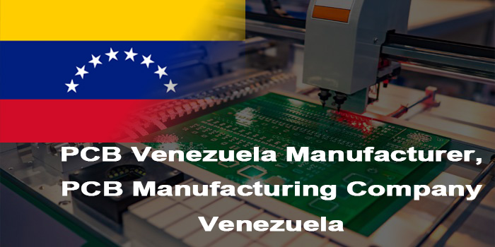
When searching for reliable PCB Venezuela manufacturer options, understanding the local market and key players is crucial. The Venezuela top 10 PCB manufacturers list serves as a valuable reference for those seeking high-quality PCB manufacturing services in the region. This guide delves into the core pain points of PCB production in Venezuela, practical solutions, and detailed evaluations of manufacturers, helping you make informed decisions. Whether you are looking for prototype or mass production services, the insights into Venezuela top 10 PCB manufacturers and industry best practices will streamline your sourcing process.
Are You Facing These PCB-Related Challenges?
- Is it difficult to find a PCB Manufacturer in Venezuela that can deliver high-quality prototypes within a short timeframe?
- Do your designs often encounter production bottlenecks due to inadequate technical support from local PCB Manufacturing Company Venezuela?
- Are you troubled by inconsistent product quality and frequent rework when cooperating with some PCB Venezuela Manufacturer?
- Does the long and unstable delivery time of local PCB Manufacturing Company Venezuela affect your project progress?
- Is it hard to get cost-effective solutions that match your budget from existing PCB Manufacturer in Venezuela?
Full-Process Guarantee from Requirement to Delivery
- Rapid Prototyping Support: We provide 24-hour fast prototyping service to solve the problem of long prototype lead time of local PCB Venezuela manufacturer, ensuring your project starts on time.
- Professional Technical Collaboration: Our team offers full-process technical support, from design review to production optimization, eliminating production bottlenecks caused by inadequate technical support.
- Strict Quality Control System: Implement full inspection for mass production and strict quality control processes, ensuring stable product quality and reducing rework rates, which solves the quality inconsistency problem of some local manufacturers.
- Efficient and Stable Delivery: With an on-time delivery rate of 99.2%, we adopt an intelligent scheduling system to ensure delivery stability and avoid project delays caused by uncertain delivery times.
- Cost-Optimized Solutions: Combined with 19 years of production experience, we provide cost-sensitive solutions tailored to your needs, helping you obtain high-cost-performance services that are difficult to get from ordinary PCB Manufacturing Company Venezuela.
Why Choose EBest Circuit (Best Technology) as Your PCB Manufacturer?
- Competitive Pricing & Cost-Sensitive Solutions: We offer competitive prices and tailor cost-sensitive solutions according to your design, helping you reduce production costs significantly.
- 24-Hour Fast Prototyping: Our urgent order handling capacity ensures 24-hour fast prototyping, meeting your tight project schedules.
- High On-Time Delivery Rate: With a 99.2% on-time delivery rate, we guarantee that your orders are delivered as scheduled, avoiding project delays caused by late shipments.
- Superior Quality Assurance: We implement full inspection for batch production and adopt strict quality control processes, ensuring stable and reliable PCB quality.
- 19 Years of Production Experience: With 19 years in the PCB manufacturing industry, we have rich experience in solving various production challenges and can help you optimize costs effectively.
- Free DFM Analysis: We provide free Design for Manufacturability (DFM) analysis to optimize your design, improve production efficiency, and reduce unnecessary costs.
- Complete International Certifications: We hold ISO9001:2015, ISO13485:2016, REACH, RoHS, and IATF16949 certifications, ensuring our products comply with international quality and environmental standards.
- Customer-Centric Service: Our team is committed to providing attentive and professional services, responding to your inquiries and needs promptly throughout the cooperation process.
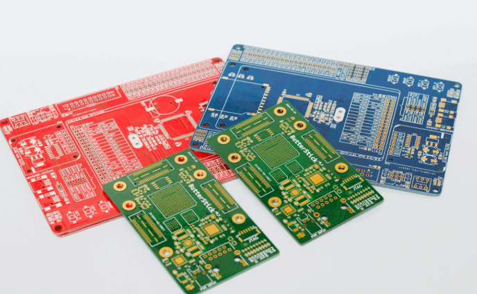
Top PCB Manufacturers in Venezuela
| Company Name | Main Business | Core Advantages | Process Capability & Delivery Time |
| Best Technology Circuit Co., Limited (EBest Circuit Co., Limited) | PCB prototype, mass production, HDI board, rigid-flex board, custom PCB manufacturing | 19 years of experience, 24-hour fast prototyping, 99.2% on-time delivery rate, multiple international certifications, free DFM analysis | Process capability: 1-64 layers PCB, HDI, blind/buried vias, impedance control; Delivery time: Prototype 24h-3days, mass production 5-12days |
| Electrónica C.A. | Single-sided and double-sided PCB manufacturing, simple PCB assembly | Localized service, fast response to small orders, compliance with COVENIN standards | Process capability: 1-2 layers PCB, FR-4 material; Delivery time: 7-15days |
| Tecnología de Circuitos Imprimidos, C.A. (TECI) | Double-sided and 4-layer PCB manufacturing, industrial control PCB production | Rich experience in industrial PCB, strict local quality inspection, stable supply capacity | Process capability: 2-4 layers PCB, impedance control optional; Delivery time: 10-20days |
| Componentes Electrónicos Venezuela, C.A. (CEV) | PCB prototype, small-batch PCB production, electronic component matching | One-stop service of PCB and components, flexible order acceptance, localized after-sales service | Process capability: 1-4 layers PCB; Delivery time: 5-12days for prototype, 12-20days for small batch |
How to Evaluate the Production Capacity of PCB Venezuela Manufacturer?
Evaluation Guide to Production Capacity of PCB Venezuela manufacturer:
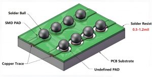
- Comprehensive process coverage evaluation: Confirm the maximum stably producible PCB layers and maturity of special processes (HDI, blind/buried vias). Request process parameter sheets or samples to verify line width/line spacing, via diameter meet design requirements.
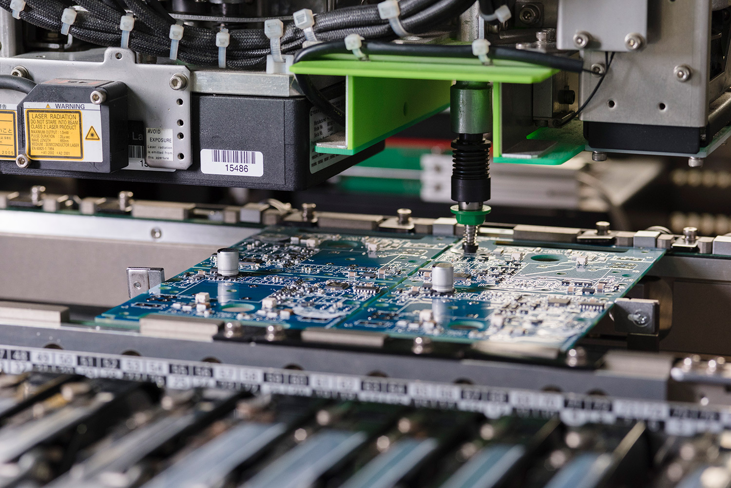
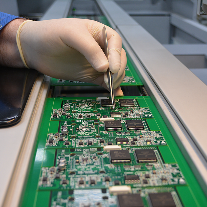
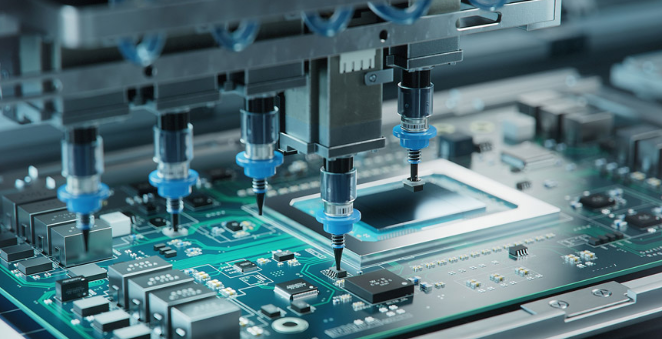
- Detailed equipment inspection: Focus on core production and testing equipment configuration. Confirm 3D AOI (for 01005 component deviation detection) and X-Ray (for internal defect inspection) for testing; check high-precision CNC drilling machines and automatic electroplating lines for production stability.
- Quality management system verification: On the basis of ISO9001:2015, ISO13485:2016 and COVENIN certifications, review quality manuals, internal audit records and non-conforming product handling processes to ensure the system is effectively implemented.
- Production scale and mass production capacity assessment: Request recent 3-month production capacity reports (daily output, production lines, utilization rate). Conduct on-site inspections for mass production orders to confirm site, personnel and raw material inventory meet continuous supply needs.
- Technical team capability evaluation: Test pre-production DFM analysis capability with design drawings; understand the team’s response speed and solution professionalism to technical problems during cooperation.
- Industry service experience investigation: Request detailed successful cases in your field; contact 1-2 reference customers to verify quality control, delivery timeliness and after-sales support.
How to Evaluate the Delivery Time of PCB Manufacturing Company Venezuela?
Evaluation Guide to Delivery Time of PCB Manufacturing Company Venezuela:
- Confirm the standard delivery cycle for different types of orders (prototype, small batch, mass production) and whether it matches your project schedule.
- Investigate the on-time delivery rate of the manufacturer in the past 12 months and check relevant customer feedback.
- Understand the emergency response capability, including whether it can provide fast delivery services for urgent orders.
- Verify the stability of the supply chain, such as the supply capacity of raw materials and the risk resistance of the production line.
- Check whether there is a perfect order tracking system to realize real-time monitoring of the production progress.
- Understand the handling mechanism for delayed delivery to ensure that your rights and interests are protected.
FAQs of Venezuela PCB Manufacturing
Q1: Why is it so hard to find reliable PCB manufacturing services inside Venezuela?
A1: Local fabrication capacity is limited, and many shops cannot offer multilayer, HDI, or advanced material options. Most engineers solve this by partnering with overseas manufacturers that provide stable lead times, consistent quality, and DDP shipping. Best Technology supports Venezuelan buyers with FR4, aluminum, flex, rigid-flex, and ceramic PCBs, and we manage customs clearance so customers receive boards directly without logistics uncertainty.
Q2: How long does it usually take to get PCBs delivered to Venezuela from a global supplier?
A2: Standard delivery runs between 7–12 days for prototypes and 10–18 days for small-batch production. The timeline depends on board complexity, surface finish, and selected shipping method. To streamline delivery, we recommend planning stack-up early, confirming Gerber accuracy, and using Express shipping for urgent R&D projects. Best Technology provides 24-hour and 48-hour fast-turn fabrication for simple FR4 and flex boards to help reduce project delays.
Q3: Are multilayer or high-frequency PCBs expensive to import into Venezuela?
A3: Costs increase with layer count, material grade (Rogers, PTFE, Megtron), and controlled impedance requirements. However, many engineers optimize cost by consolidating orders, simplifying stack-ups, or selecting equivalent RF laminates when possible. We provide engineering suggestions before production, propose cost-efficient materials, and share real-time quotes so buyers can avoid unexpected expenses.
Q4: How do Venezuelan engineers handle customs or tax issues when ordering PCBs from abroad?
A4: Most rely on DDP or door-to-door logistics to bypass paperwork. This avoids delays caused by documentation errors or local customs backlog. Best Technology can ship under DDP terms, handle HS codes, prepare commercial invoices, and manage all export documents. Customers only need to confirm their address, and we ensure boards arrive smoothly.
Q5: Can Venezuelan companies get PCBA services, not only bare PCBs?
A5: Yes. Many global suppliers provide full PCBA, including component sourcing, SMT/THT assembly, and functional testing. This is especially helpful in Venezuela where component availability is inconsistent. Our team sources global components (Digikey, Mouser, Arrow, local Asian markets), performs SMT/THT assembly, runs AOI/X-ray/ICT, and ships finished boards ready for installation.