PCB fiducial markers are solid copper reference pads on a printed circuit board, not drilled holes, used by automated assembly machines for optical alignment. This article provides a comprehensive guide to PCB fiducial guidelines, explaining their critical role, proper implementation, and common pitfalls to ensure flawless surface mount technology (SMT) assembly.
Even a perfectly designed PCB can suffer low assembly yield due to inaccurate SMT placement caused by improperly implemented fiducial markers PCB.
- Low First-Pass Yield: Poor fiducial markers PCB lead to placement errors and immediate solder defects.
- Inconsistent Assembly Quality: Missing or unreliable PCB fiducial marks cause batch-to-batch placement variation.
- Wasted Time and Cost: Incorrect PCB fiducial placement creates hidden assembly issues that delay production.
- Limitation with Advanced Packages: High-density BGAs, QFNs, and 01005 parts demand precise PCB fiducial markers to assemble correctly.
- Rigid Panelization Issues: Improper fiducials on PCB panels cause array-wide misalignment and repeated defects.
These issues can be avoided by applying professional PCB fiducial guidelines from the earliest design stage.
- Design for Manufacturability Review: We verify your design against strict PCB fiducial requirements before fabrication.
- Process-Optimized Fabrication: Gold fiducial markers and pads are produced with high contrast for stable machine vision.
- Panelization Expertise: Optimized fiducial layouts ensure accurate placement across all boards in a panel.
- Support for All Package Types: Local fiducials enable precise assembly of fine-pitch and high-density components.
- End-to-End Guidance: We define what fiducial markers are made of, where to place them, and how many to use.
At EBEST CIRCUIT (BEST TECHNOLOGY), we specialize in transforming complex designs into reliably manufactured products. Our expertise extends from high-precision PCB fabrication to full turnkey assembly, with a deep focus on DFM (Design for Manufacturability) principles—including mastering the art and science of PCB fiducial markers. We ensure your boards are not just designed correctly, but are optimized for flawless, high-yield production. Pls feel free to contact our engineering team at sales@bestpcbs.com to review your next custom printed circuit board project.
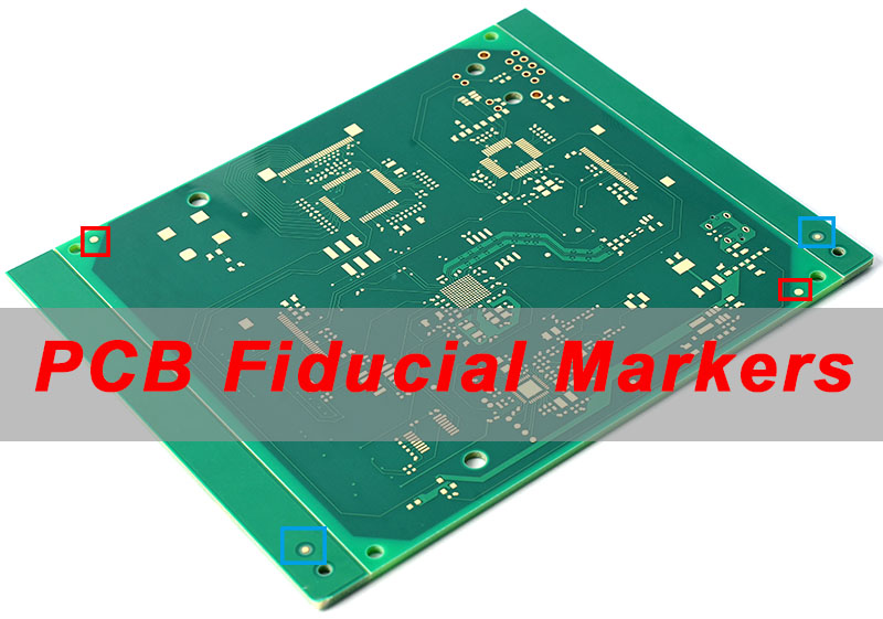
What Are PCB Fiducial Markers?
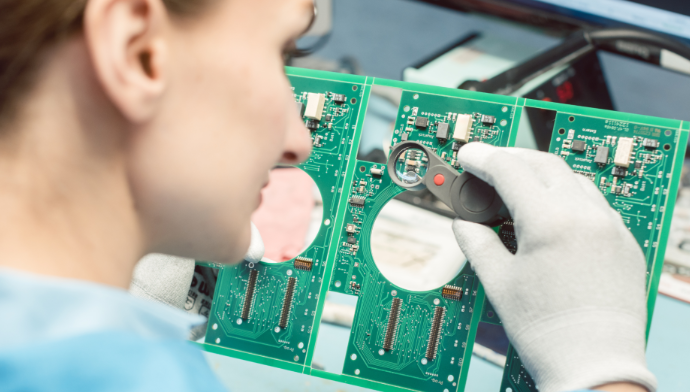
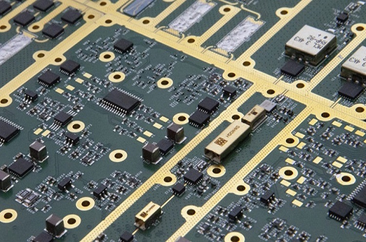
In essence, a PCB fiducial marker is a physical “target” on a circuit board. In the realm of electronics manufacturing, what is a fiducial marker? It is a precisely fabricated feature, typically a small exposed copper pad, that provides a fixed reference coordinate system for automated optical inspection (AOI) and SMT pick-and-place machines.
- Machine Vision Reference: The machine camera locates these markers to accurately determine the board’s position, rotation, and scaling in the horizontal (X-Y) plane.
- Compensation for Variance: They compensate for inherent minor fabrication tolerances (like stretch or shrinkage) and mechanical handling misalignments in the loader.
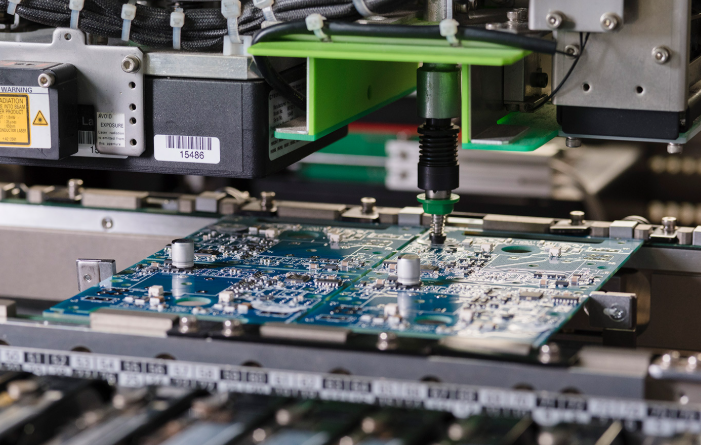
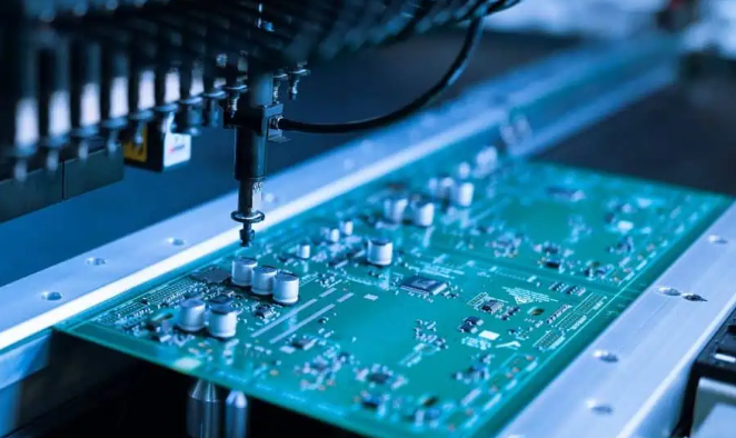
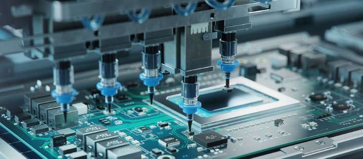
- Critical for Automation: They are fundamental for the speed and precision of modern, fully automated assembly lines.
In summary, a position shown as a circle with a hole through it indicates a drilled hole, while an optical fiducial is a solid copper pad without a hole. Understanding PCB fiducial markers meaning is the first step to leveraging their power for reliable manufacturing.
What are the Types of Fiducial Markers in PCB?
Types of Fiducial Markers in PCB by Material
- 1. Bare Copper Fiducial Markers
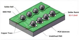
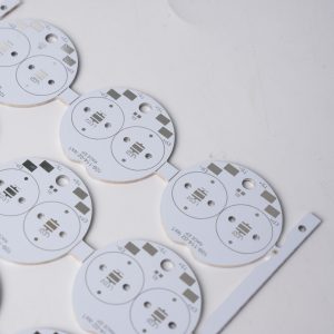
Solid copper pads with no solder mask or plating, providing high contrast for machine vision and representing the most commonly used fiducial type in SMT assembly.
- 2. Gold Fiducial Markers
Copper pads finished with ENIG or other gold plating, offering excellent contrast and oxidation resistance, often used in high-reliability or long-storage applications.
- 3. Tin-Plated Fiducial Markers
Copper pads with a tin finish, lower in cost but less consistent in optical contrast, making them less suitable for high-precision placement.
- 4. Silver-Plated Fiducial Markers
Fiducials with an immersion silver finish, providing good initial visibility but prone to oxidation, requiring careful storage and process control.
- 5. Non-Metallic Fiducial Markers (Not Recommended)
Markers created using silkscreen or solder mask features, which generally lack sufficient contrast and are not reliable for SMT machine vision systems.
In closing, bare copper or gold fiducial markers deliver the most stable and repeatable performance in automated PCB assembly.
In PCB design and SMT assembly, fiducial markers are commonly classified by function and scope, not by material alone. The main types of fiducial markers in PCB are as follows:
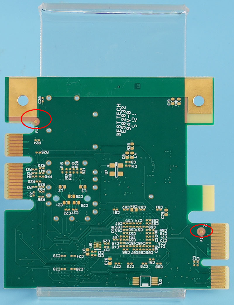
- 1. Global Fiducial Markers
Global fiducials are placed on the PCB or panel corners and are used by pick-and-place machines to establish the board’s overall X, Y, and rotation reference before component placement.
- 2. Local Fiducial Markers
Local fiducials are positioned close to high-precision components such as BGAs, QFNs, or fine-pitch ICs, allowing the machine to correct localized distortion and achieve tighter placement accuracy.
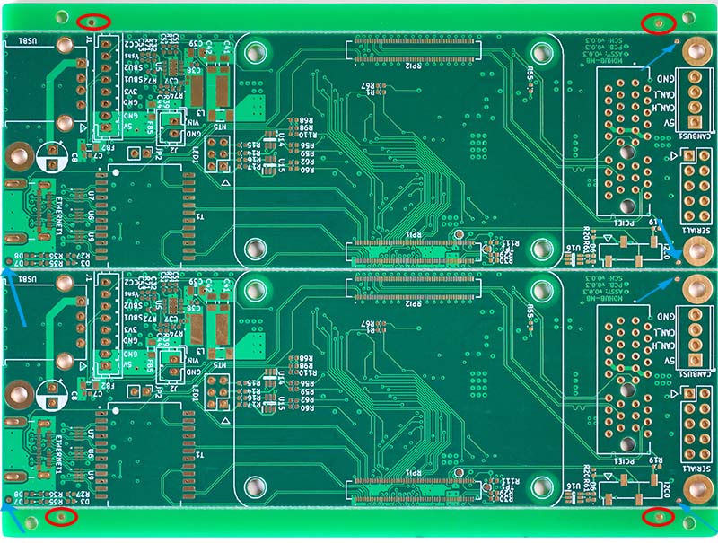
- 3. Panel Fiducial Markers
Panel fiducials are located on panel rails or frames and are used to align the entire PCB array during automated assembly, especially in high-volume production.
- 4. Component-Level Fiducials
These fiducials are embedded directly within a component footprint for ultra-fine pitch devices, providing the highest placement accuracy when global fiducials are insufficient.
- 5. Optical Copper Fiducials (Most Common)
Solid, non-plated copper pads with solder mask clearance, optimized for machine vision recognition.
Most professional SMT lines rely on a combination of global + local fiducial markers to balance speed, accuracy, and yield.
Are PCB Fiducial Markers Necessary for PCB?
While a very simple, low-density board assembled manually might get by without them, fiducials are absolutely necessary for any serious, automated PCB production. Their necessity scales with:
- Board Complexity: High component density, fine-pitch parts (<0.5mm pitch), or BGAs demand them.
- Assembly Volume: Automated assembly for any volume beyond prototyping requires them for consistency.
- Quality Requirements: Any application where high reliability and yield are critical mandates their use. What are fiducial markers used for? Ultimately, they are used for ensuring repeatable quality.
Are PCB Fiducial Markers Placed on One Side?
The placement depends on the assembly process.
- Single-Side Assembly: Fiducial markers PCB are only required on the side being assembled.
- Double-Side Assembly: Fiducials are needed on both sides. Often, different sets of markers are used for top and bottom-side assembly to avoid confusion for the machine. The key question—are PCB fiducial markers placed on one side—is answered by your assembly process flow.
Where to Put PCB Fiducial Marker Placement on a PCB?
Strategic PCB fiducial marker placement is crucial. Follow these guidelines:
| Placement Type | Typical Location | Core Rule |
|---|---|---|
| Global Fiducials | Board or panel corners | ≥2, ideally 3 (L-shape) |
| Local Fiducials | Near critical components | Diagonal pair |
| Clear Area | Around each fiducial | 1–2 mm keep-out |
| Panel Fiducials | Panel rails | Required for panel alignment |
- Global Fiducials
Used by the pick-and-place machine to establish the board’s origin and rotation before component placement. - Local Fiducials
Applied near BGAs or fine-pitch ICs to correct localized distortion and improve placement accuracy. - Clear Area
A clean copper reference ensures stable machine vision and avoids false edge detection. - Panel Fiducials
Critical for consistent alignment across multi-board panels during high-volume SMT assembly.
How Many Fiducial Markers PCB Designs Really Need?
There is no single answer, but a robust scheme includes:
- Minimum: 2 global fiducials (detects X, Y, rotation).
- Recommended: 3 global fiducials (asymmetrical, allows detection of scaling/stretch).
- Add Local Fiducials: For every critical, high-pin-count, or fine-pitch component.
- Panel Level: At least 3 fiducials on the panel rails. A good rule is to err on the side of more reference points for complex designs.
How Are PCB Fiducial Marks Inserted During PCB Design?
They are added in the CAD software as part of the board layout. For example:
- Fiducial PCB Altium: Use the “Pad” tool, set to a non-plated through-hole (NPTH) or a surface mount pad. Place it on a dedicated mechanical layer (e.g., “Mechanical 1” or “Fiducials”) and also on the copper layer. The solder mask opening must be defined.
- Kicad Fiducial: You can create a footprint for a fiducial (containing a pad on the copper layer with appropriate solder mask expansion) and place it like any other component. The key is to define them clearly in your Gerber/ODB++ output so the fabricator understands them.
Can PCB Fiducial Markers Be Removed After PCB Fabrication?
No. Fiducials are permanent features etched into the copper layer. They are essential for the entire SMT assembly process. The idea of can PCB fiducial markers be removed after PCB fabrication is a misconception; they are integral to the board’s design for assembly.
What Are the Side Effects of Poor PCB Fiducial Placement?
Poor PCB fiducial placement directly undermines SMT precision. Consequences include:
- Misaligned solder paste deposition.
- Tombstoning of small passive components.
- Bridging on fine-pitch IC leads.
- Poor solder ball alignment on BGAs, leading to open connections.
- Dramatically reduced first-pass yield and increased cost.
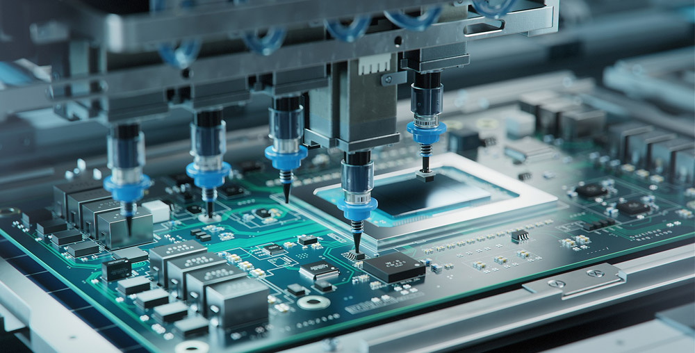
What Are Fiducial Markers Used For in PCB Assembly?
To summarize what are fiducial markers used for in the SMT line:
- Board Alignment: Correcting the board’s position in the machine.
- Paste Inspection: Providing a reference for solder paste inspection (SPI) machines.
- Component Placement: Guiding the pick-and-place head for accurate part location.
- Post-Placement Inspection: Serving as a reference for Automated Optical Inspection (AOI).
What Are the Essential PCB Fiducial Guidelines Engineers Should Follow?
Follow these core PCB fiducial guidelines:
- Size & Shape: Standard PCB fiducial size is 1.0mm to 1.5mm diameter. Use a solid filled circle.
- Material: Use bare copper with an oxidation-resistant finish (HASL, ENIG). Gold fiducial markers (ENIG) offer the best contrast and durability.
- Clearance: Ensure a solder mask clearance (annular ring) of at least 0.5-1.0mm for a clear donut shape.
- Symmetry: Avoid symmetrical placement of only two markers. Use an asymmetrical pattern.
- Consistency: Use the same type and size of fiducial across the board/panel where possible.
- Documentation: Clearly note fiducials in your fabrication and assembly drawings.
All in all, PCB fiducial markers are the unsung heroes of reliable, high-yield SMT assembly, providing the critical visual reference that bridges your design intent to physical reality. This guide has detailed their purpose, types of fiducial markers in PCB, and the essential guidelines for their effective use. While the concept shares its name with what is a fiducial marker in physics or fiducial marks in aerial photography—all referring to fixed reference points—in PCB manufacturing, their precision directly translates to product quality and cost. Implementing robust fiducial design is a hallmark of a design engineered for manufacturability.
For designers and engineers, partnering with a manufacturer that understands these nuances is key. EBEST CIRCUIT (BEST TECHNOLOGY) integrates this expertise into every stage, from DFM review of your fiducial PCB Altium or Kicad fiducial designs to precision fabrication and assembly. We ensure your reference points—and your final product—are positioned for success. For a consultation on your next project, pls feel free to contact us at sales@bestpcbs.com.
FAQs
- What Is DK and DF in PCB?
DK (Dielectric Constant) and DF (Dissipation Factor) are material properties of the PCB substrate. DK affects signal speed/impedance; DF affects signal loss. They are unrelated to fiducials but critical for high-frequency design. - Do PCBs Need a Ground Plane?
Highly recommended for most designs. It provides a stable reference voltage, reduces EMI, improves signal integrity, and aids heat dissipation. It’s essential for controlled impedance and noise-sensitive circuits. - How to Avoid PCB Exposure?
This refers to preventing unintended exposure of copper (e.g., from solder mask misregistration). Work with a reliable fabricator (like EBEST), provide accurate design files with sufficient solder mask dams, and request DFM feedback.