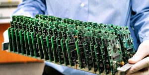
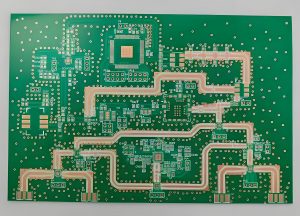
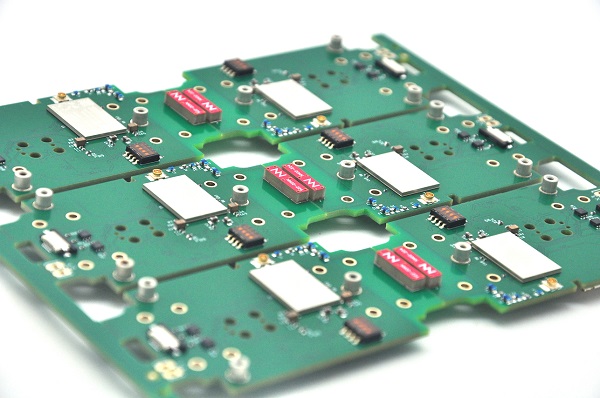
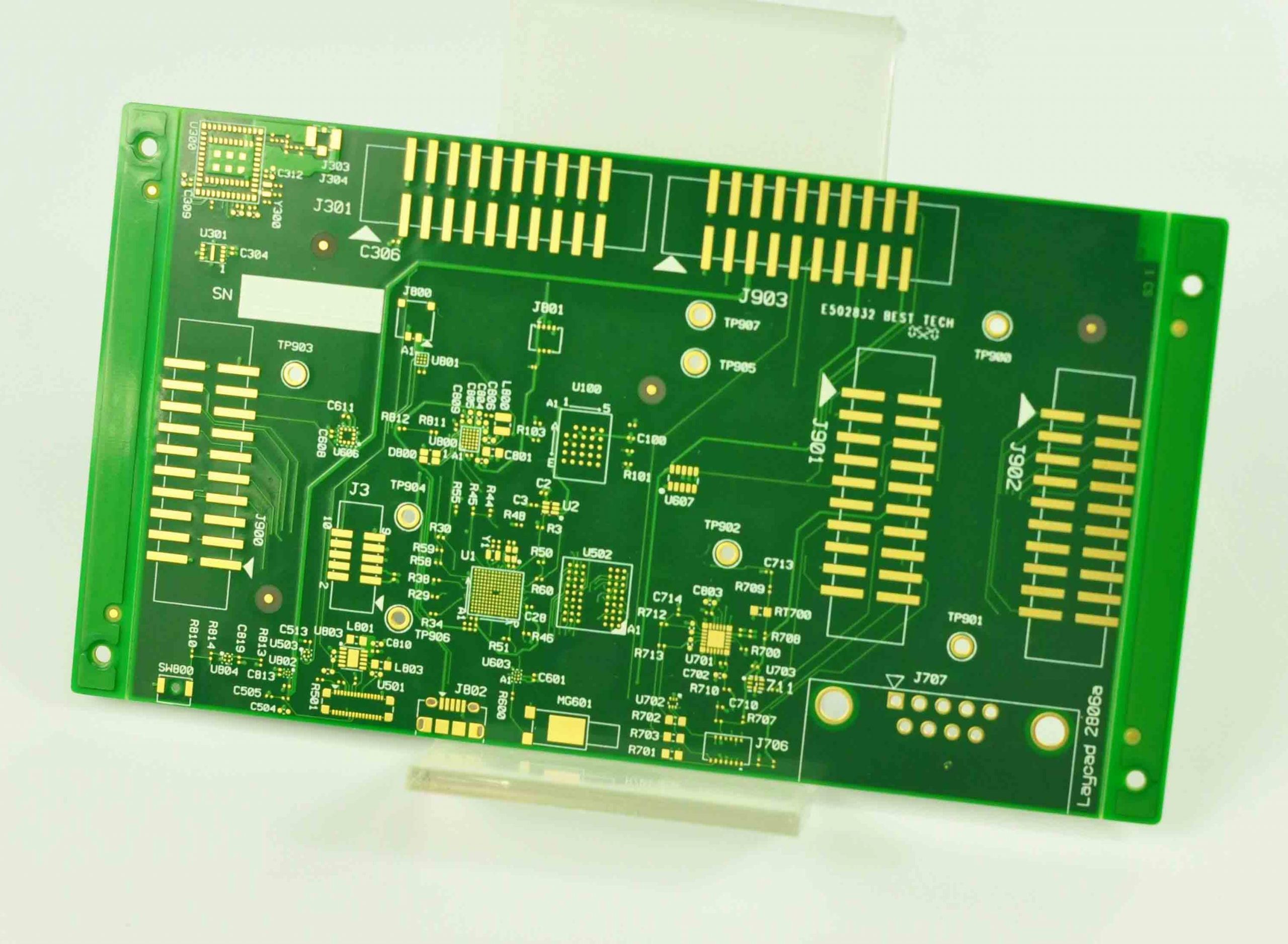
With the development of society, the demand for heavy copper PCBs in different industries has become increasingly greater. At present, heavy copper PCBs have been widely used in various electronic industries. Generally speaking, heavy copper technology can realize complex switches in a limited space, combine circuits with high current levels, and is conducive to heat dissipation. Multilayer and double-sided are the most common designs we know. More importantly, heavy copper PCB technology makes it possible to combine good layout structures on the outer layer and Heavy copper layers on the inner layer.
What is a heavy copper PCB?
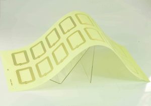
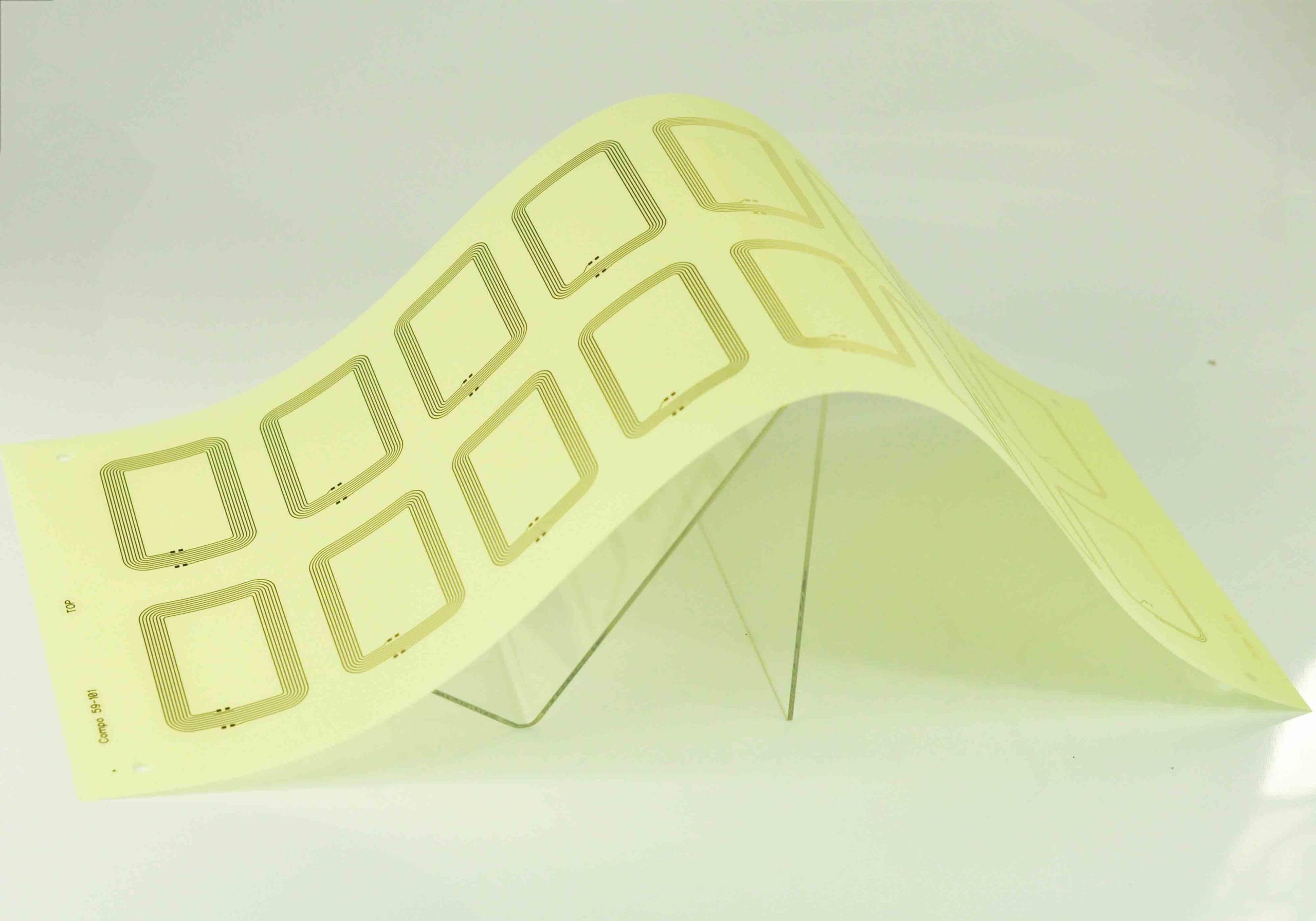
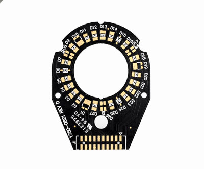
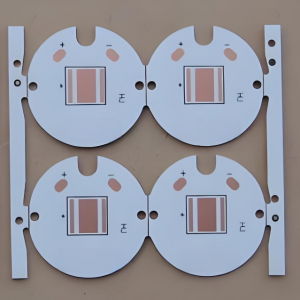
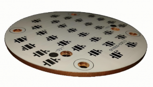
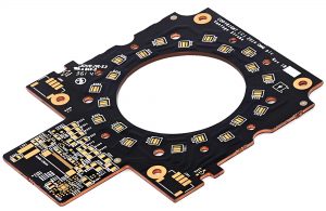
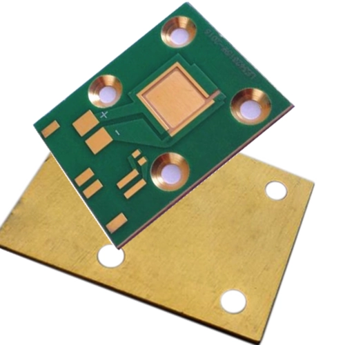
Heavy copper PCB is a special printed circuit board (PCB) characterized by a very high concentration of copper, usually up to 200 ounces per square foot, and the copper content of the inner and outer layers of the circuit board is above 3 ounces (oz), which enables heavy copper PCBs to conduct extremely high currents, achieve good heat distribution, and realize complex circuit layouts in a limited space.
In the design and manufacturing process of heavy copper PCBs, thermal stress handling is an important consideration. Engineers need to eliminate thermal stress as much as possible to maintain the circuit while minimizing the power budget, while taking into account environmentally friendly design.
With the development of PCB manufacturing process, modern manufacturing technology such as the use of aluminum PCB can better handle thermal stress problems.
The heat dissipation capacity of Heavy copper PCB is better than the traditional solution of using external heat sink, because it prints the heat sink directly on the circuit board during the manufacturing process, and achieves rapid heat transfer through conductive through-holes, thereby improving heat dissipation performance.
In general, Heavy copper PCB is a high-performance electronic component carrier, which provides an ideal solution for applications requiring high power and high reliability through its high copper content and optimized thermal management characteristics.
What is the difference between PCB and Heavy copper PCB?
Copper board and Heavy copper board look similar in name, and people tend to think that they are the same PCB, but in fact they refer to different things.
1. PCB:
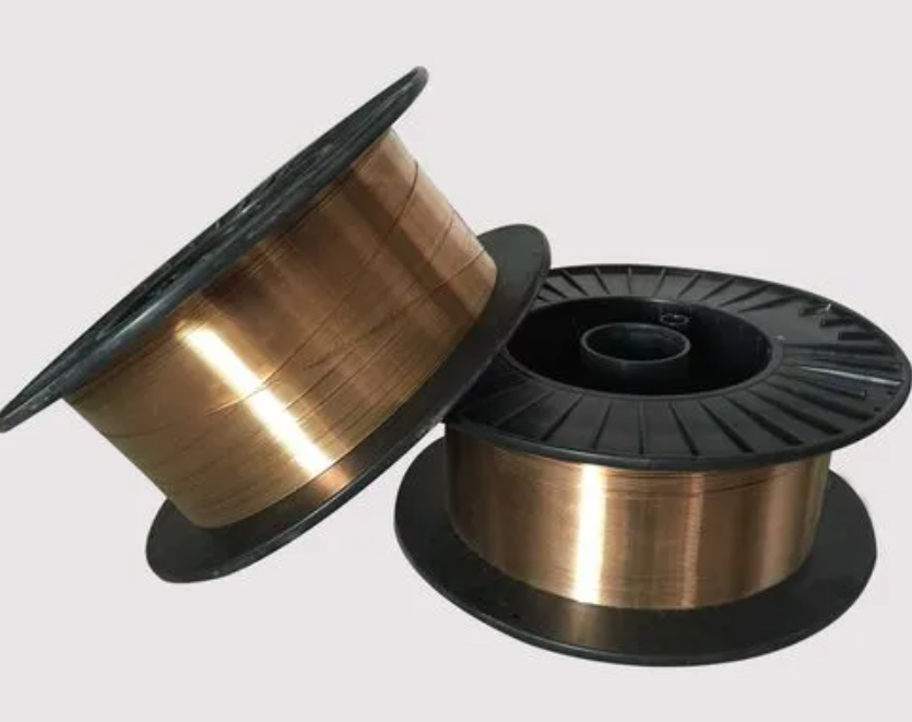
PCB refers to a copper-based PCB. The use of copper as a substrate is to better dissipate heat and extend the life of components on the PCB. The copper substrate is to allow heat to be quickly transferred from the PCB to the outside, such as a heat sink or a metal casing. Because the thermal conductivity of copper is several times that of aluminum or other metals, up to 401W/MK.
2. Heavy copper PCB:
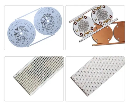
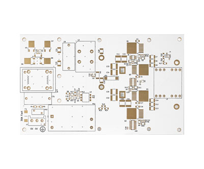
Heavy copper PCB refers to PCB with copper thickness exceeding 3OZ. The substrate can be aluminum or FR4. Heavy copper is to enable PCB to carry large current. Please note that Heavy copper here does not refer to the thickness of PCB, but the thickness of copper foil on PCB. Both aluminum PCB and FR4 PCB can thicken the copper foil.
What is the maximum copper thickness on Heavy copper PCB?
The maximum thickness of copper on Heavy copper PCB can reach 20oz.
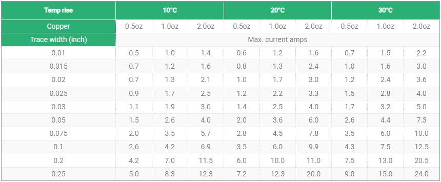
In circuit board design and manufacturing, copper thickness is an important parameter, which directly affects the electrical performance, heat dissipation capacity and mechanical strength of the circuit board. For applications that need to carry large currents, it is necessary to choose a thicker copper layer.
The copper layer thickness of Heavy copper ultra-thick PCB is generally between 2oz and 20oz. This range of copper layer thickness can ensure the stability and reliability of the circuit board while providing good heat dissipation performance.
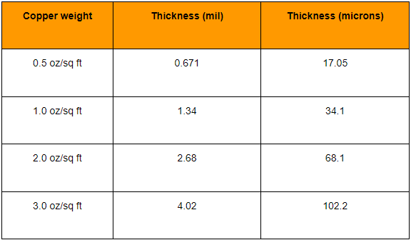
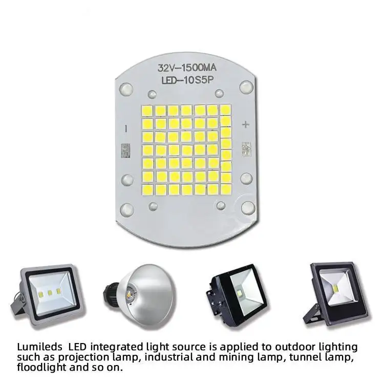
In practical applications, according to international standards, the copper thickness of PCB boards can be divided into standard copper thickness and non-standard copper thickness. Standard copper thickness includes 1oz (35um) and 2oz (70um), while non-standard copper thickness covers 0.5oz (17um), 3oz (105um) and 4oz (140um). For some special applications, such as high-power LED lights, electronic high-frequency circuits, etc., a higher copper thickness may be required. At this time, non-standard copper thickness will be selected, up to 20oz.
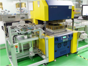
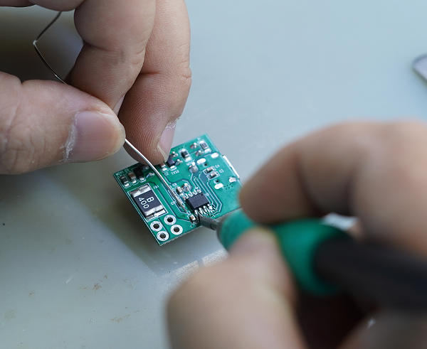
During the manufacturing process, a Heavy copper foil is first adhered to the substrate, and then the circuit pattern is transferred to the copper foil through a photolithography process. Then chemical etching is performed to remove excess copper, and finally the thickness of the copper layer is further increased through an electroplating process to ensure that the Heavy copper PCB can meet the requirements of high current and high power applications.
Finally, surface treatment is performed to protect the copper circuit from oxidation and corrosion. Common surface treatment methods include hot air leveling (HASL), lead-free tin spraying, nickel gold (ENIG), etc. During the entire manufacturing process, process parameters must also be strictly monitored to ensure the uniformity and thickness consistency of the copper layer.
What are the advantages of Heavy copper PCBs?
1. Heavy copper PCBs have better current conductivity and can withstand excessive current loads. Because thicker copper wires have higher current carrying capacity, their current carrying capacity can be increased by increasing the copper wire width.
2. Heavy copper inner layers are ideal power distribution layers in multi-layer PCBs, which minimize ground bounce and power supply noise
3. Improve thermal performance and increase heat dissipation. Can withstand repeated thermal cycles during manufacturing and assembly.
4. Provide high mechanical strength in connector locations and plated through holes.
5. Due to the presence of copper layers, the size of the circuit board is reduced.
What are the disadvantages of Heavy copper PCBs?
1. Heavy copper PCBs are more expensive to manufacture than standard PCBs because more specialized equipment and richer expertise are required.
2. Heavy copper PCBs are more difficult to process because the PCBs may be heavier and bulkier than other PCBs.
What are the properties of Heavy copper PCBs?
High mechanical strength: After Heavy copper is applied to the circuits and vias of the board, the printed circuit board has super high mechanical strength, and the weather resistance of the circuit board and electrical system is more stable and has a high melting point. Hot melt welding methods such as oxygen blowing can be used, and it is not easy to become brittle at low temperatures. Even in an extremely corrosive atmospheric environment, Heavy copper PCBs can form a strong, non-toxic passivation protective layer.
Excellent weather resistance: Because Heavy copper PCB boards support the selection of a variety of dielectric materials. It improves the overall weather resistance of the board and can ensure the stability of circuit transmission signals under certain high temperature or extreme special environments.
Thermal management: With the advancement of modern technology, PCBs are becoming more and more complex, and high-density currents increase the difficulty of thermal management. Excessive temperature will affect the normal operation of electronic equipment and even cause damage. Heavy copper PCB boards can provide stronger heat dissipation capabilities. With heat sinks and copper plating on through holes, the heat generation of the board can be greatly reduced.
Excellent current conductivity: In the operation of electronic equipment, Heavy copper printed circuit boards are excellent current conductors that can connect and transmit power between various boards.
Diversity: Plating of Heavy copper circuits allows Heavy copper PCB manufacturers to increase the copper weight of via sidewalls and plated holes, thereby reducing the number of layers and occupied space.
Ductility: Heavy copper PCBs have the best ductility and are not limited by processing temperature.
High performance: Heavy copper plating integrates high current and control circuits, allowing high density with a simple board structure.
Where are Heavy copper PCBs used?
1. Automotive electronics

2. Grid switching systems
3. Power line monitors
4. Security and signal systems
5. Radar monitoring systems
6. Industrial control
7. Aerospace
8. Telecommunications
9. Medical devices
Conclusion:
In PCB production, Heavy copper PCBs require special processes, are difficult to operate, and have certain technical barriers, so the production cost of Heavy copper PCBs is higher than other ordinary circuit boards. Although the price is not cheap, the quality and service are the best.
BEST Technology has more than 18 years of PCB manufacturing experience. Focusing not only on fast PCB prototyping and PCB assembly, but also on small and medium batch PCB manufacturing, customer satisfaction is our goal, we will do our best to manufacture your circuit boards in the highest quality to meet your needs, and are committed to complying with the most stringent standards in PCB manufacturing and assembly.