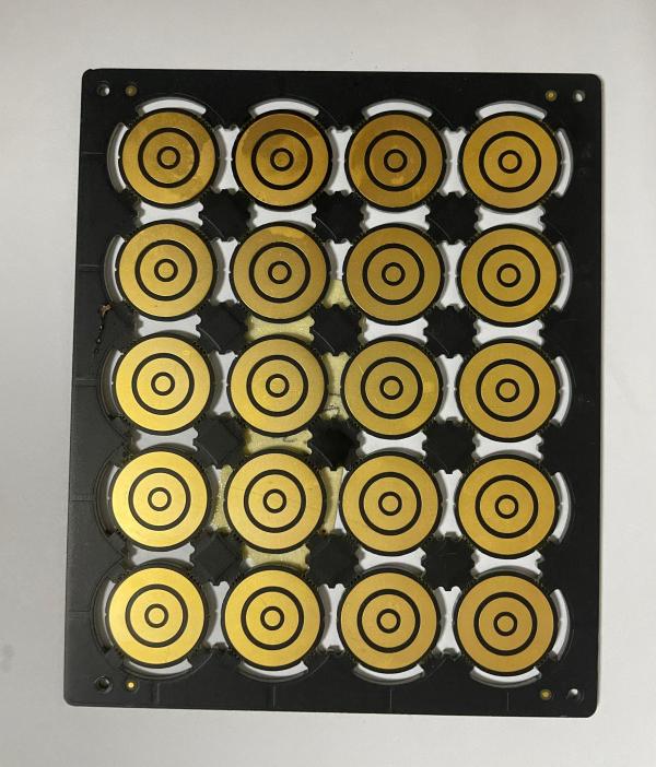
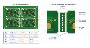
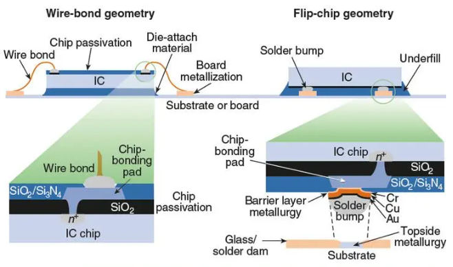
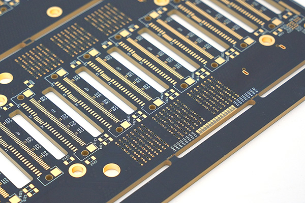
Best is mainly engaged in the production of High frequency pcb communication circuits, high-speed, microwave and radio frequency printed circuit boards, mainly in sample making and small and medium batches. The main products are: microwave radio frequency high-frequency boards, Rogers high-frequency boards, Rogers multi-layer high-frequency mixed-pressure boards, Rogers radio frequency boards, Taconic microwave boards, Taconic multi-layer circuit boards, Arlon microstrip antenna boards, ARLON high-frequency boards, F4BM antenna boards, F4BM multi-layer mixed-pressure boards, radio frequency amplifier PCB boards, HDI precision multi-layer boards, serving domestic and foreign high-tech enterprises and scientific research institutions.
What is a high frequency pcb communication circuits
High frequency pcb communication circuits to a circuit board with an operating frequency in the high frequency band (usually greater than 300MHz or a wavelength less than 1 meter), which is mainly used to transmit high-frequency signals and data. This type of circuit board is widely used in radio frequency (RF) and microwave fields, such as communication equipment, radar systems, satellite communications, and high-speed data transmission systems.

What is a high frequency pcb communication circuits
The characteristics of high-frequency circuits include challenges such as transmission line effects, signal integrity issues, and electromagnetic interference (EMI). Due to the short wavelength of high-frequency signals, traditional low-frequency circuit design methods are no longer applicable, and special design and processing methods are required to ensure the performance and stability of the circuit.
High-frequency circuit boards are produced on microwave substrate copper-clad boards using ordinary rigid circuit board manufacturing methods or special processing methods. They need to have high-quality electrical properties and chemical stability to meet the requirements of high-frequency signal transmission.
Definition of high frequency pcb communication circuits
High-frequency circuit board, as a special circuit board, is mainly suitable for occasions with high electromagnetic frequency, especially in the fields of high frequency (frequency greater than 300MHz or wavelength less than 1 meter) and microwave (frequency greater than 3GHz or wavelength less than 0.1 meter).
It is a circuit board made on a microwave substrate copper-clad board by adopting some manufacturing processes or special processing methods of ordinary rigid circuit boards. Generally speaking, when the frequency of the circuit board reaches above 1GHz, it can be defined as a high-frequency board.
With the rapid development of science and technology, more and more equipment designs have begun to involve microwave frequency bands (>1GHz) and even expanded to the millimeter wave field (such as 77GHz), especially in popular applications such as 77GHz millimeter wave antennas on vehicles.
This trend not only promotes the continuous increase in frequency, but also puts higher requirements on the substrate of the circuit board.
For example, the substrate material needs to have excellent electrical properties, stable chemical properties, and as the frequency of the power signal increases, the loss on the substrate must be extremely small. Therefore, the importance of high-frequency boards is becoming more and more prominent.
Advantages of high frequency pcb communication circuits
The main advantages of high frequency pcb communication circuits include efficient data transmission, strong anti-interference ability, high-frequency bandwidth and high reliability.
- high frequency pcb communication circuits can achieve efficient data transmission. High-frequency signals have a short cycle and can transmit more information per unit time, so they have the advantage of large-capacity transmission. In addition, high-frequency signals can achieve fast signal processing and are suitable for application scenarios that require high-speed data transmission and high real-time requirements.
- high frequency pcb communication circuits have strong anti-interference capabilities. Due to the short wavelength of high-frequency signals, they can better avoid external interference and attenuation and have strong anti-interference capabilities. This makes high-frequency signals have advantages in fields such as wireless communications and radar systems, and can achieve stable signal transmission and reception.
- high frequency pcb communication circuits also have the advantage of high-frequency bandwidth. High-frequency signals correspond to a larger frequency range and can provide higher bandwidth than low-frequency signals. This means that more data can be transmitted, thereby supporting higher data rates and richer media content.
- High reliability of high frequency pcb communication circuits is also one of its advantages. The use of high-quality materials and manufacturing processes can effectively resist external interference and oxidation corrosion, ensure stable performance in high temperature environments, and thus extend the service life of the circuit board.
Classification of high frequency pcb communication circuits
Classification by material:
- Organic materials: including phenolic resin, glass fiber/epoxy resin, Polyimide, BT/Epoxy (bismaleimide triazine/epoxy resin), etc.
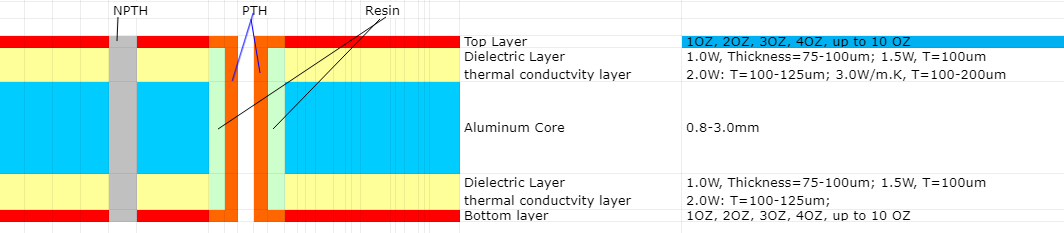
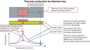
- Inorganic materials: mainly including aluminum, copper-invar-copper, ceramic, etc. These materials are mainly selected for their excellent heat dissipation function.
Classification by the hardness of the finished product:
- Rigid PCB: has a solid structure and stable performance.
- Flexible PCB: has flexibility and bendability, suitable for occasions requiring flexible wiring.
- Rigid-Flex PCB: It combines the characteristics of rigid and flexible boards, and has higher design flexibility and wide application.
Classification by structure:
- Single-sided board: A circuit board with a conductive layer on only one side.
- Double-sided board: Both sides are coated with conductive layers, separated by insulating materials in the middle.
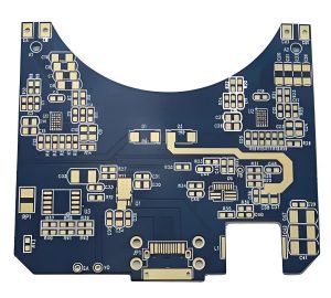
- Multilayer board: It is composed of multiple conductive layers and insulating layers, and has higher circuit integration and reliability.
Classification by use:
- Communication board: It is used in various communication equipment and systems.
- Consumable electronic board: It is commonly found in consumer electronic products.
- Military board: A circuit board that meets special requirements in the military field.
- Computer board: A circuit board used in computer hardware.
- Semiconductor board: A circuit board used in the manufacturing and testing process of semiconductors.
- Electrical test board: A circuit board used in electronic testing and measurement equipment.
How to choose high-frequency circuit board high-speed board
When choosing PCB board, you must find a balance between meeting design requirements, mass production and cost. In short, the design requirements cover two aspects: electrical performance and structural reliability. Especially when designing ultra-high-speed PCB (frequency greater than GHz), the choice of board is particularly important. For example, the commonly used FR-4 material will have a significantly increased dielectric loss (Df, i.e., Dielectric Loss) at a frequency of several GHz, and may no longer be applicable.
Taking the 10Gb/S high-speed digital signal as an example, this signal can be regarded as the superposition of multiple sinusoidal wave signals of different frequencies. Therefore, the 10Gb/S signal contains multiple components of different frequencies: such as a 5GHz fundamental signal, a 3rd-order 15GHz signal, a 5th-order 25GHz signal, and a 7th-order 35GHz signal. In order to ensure the integrity of digital signals, maintain the steepness of the upper and lower edges of the signals, and be compatible with the low-loss, low-distortion transmission of RF microwaves (the high-frequency harmonic part of the digital signal reaches the microwave frequency band), the selection of materials for high-speed digital circuit PCBs has many similarities with the needs of RF microwave circuits.
In actual engineering operations, the selection of high-frequency boards seems simple, but the factors that need to be considered are quite complex. Through the introduction of this article, PCB design engineers or high-speed project leaders can have a deeper understanding of the characteristics and selection of boards. Understand the electrical properties, thermal properties, reliability and other characteristics of the board, and use the stacking design reasonably to create products with high reliability and excellent processability, and achieve the best balance of various factors.
Composition and key components of high frequency pcb communication circuits
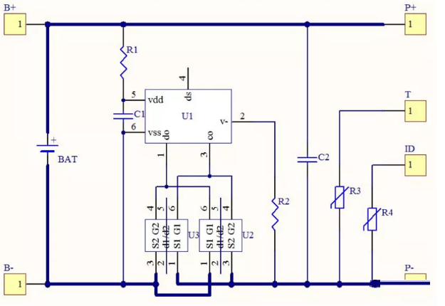
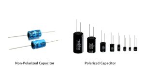
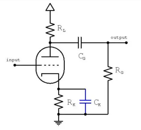
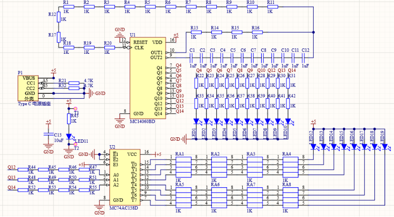
High frequency pcb communication circuits are basically composed of passive components, active devices and passive networks. Passive components include resistors, capacitors and inductors, which mainly exhibit resistance characteristics at low frequencies, but also exhibit reactance characteristics at high frequencies. Active devices such as high-frequency triodes have the characteristics of high gain, high frequency response and low noise, and are widely used in television, radio communication, radar and other fields.
Application of high frequency pcb communication circuits
High frequency pcb communication circuits are widely used in long-distance communication systems, with a communication distance of up to thousands of kilometers, and are often used to maintain communication between aircraft and bases. It occupies a high-frequency band of 2~30MHz, uses skywave propagation, and can propagate over long distances. Modern airborne high-frequency communication systems usually use single-sideband communication systems, which can greatly compress the occupied frequency band and save transmission power. However, high-frequency communication is also susceptible to electrical interference such as ionospheric disturbances and lightning, generating radio background noise, and there is fading, and the signal is sometimes strong and sometimes weak.
Design Guidelines for High Frequency PCB Communication Circuits

Design Guidelines
High Frequency PCB Communication Circuits
- How to avoid high-frequency interference?
The basic idea of avoiding high-frequency interference is to minimize the interference of the electromagnetic field of high-frequency signals, which is the so-called crosstalk. You can increase the distance between high-speed signals and analog signals, or add ground guard/shunt traces next to analog signals. Also pay attention to the noise interference of digital ground to analog ground.
- How to solve the signal integrity problem in high-frequency communication PCB design?
Signal integrity is basically an impedance matching problem. The factors that affect impedance matching include the architecture and output impedance of the signal source, the characteristic impedance of the trace, the characteristics of the load end, and the topology of the trace. The solution is to rely on termination and adjust the topology of the trace.
- How is the differential wiring method implemented?
There are two points to note when wiring differential pairs. One is that the length of the two lines should be as equal as possible, and the other is that the spacing between the two lines (this spacing is determined by the differential impedance) should remain unchanged, that is, they should be kept parallel. There are two parallel methods, one is that two lines run on the same routing layer (side-by-side), and the other is that two lines run on two adjacent layers (over-under). Generally, the former side-by-side (side by side, shoulder to shoulder) is more commonly used.
- How to implement differential routing for clock signal lines with only one output end?
To use differential routing, it must be meaningful if both the signal source and the receiving end are differential signals. Therefore, differential routing cannot be used for clock signals with only one output end.
- Can a matching resistor be added between the differential line pairs at the receiving end?
The matching resistor between the differential line pairs at the receiving end is usually added, and its value should be equal to the value of the differential impedance. This will improve the signal quality.
- Why should the routing of differential pairs be close and parallel?
The routing method of differential pairs should be appropriately close and parallel. The so-called appropriate proximity is because this spacing will affect the value of differential impedance, which is an important parameter for designing differential pairs. Parallelism is also required because the consistency of differential impedance must be maintained. If the two lines are sometimes far away and sometimes close, the differential impedance will be inconsistent, which will affect the signal integrity and timing delay.
- How to deal with some theoretical conflicts in actual wiring?
Basically, it is right to separate the analog/digital ground. It should be noted that the signal routing should try not to cross the split place (moat), and the return current path of the power supply and signal should not be too large.
The crystal oscillator is an analog positive feedback oscillation circuit. To have a stable oscillation signal, the loop gain and phase specifications must be met. The oscillation specification of this analog signal is easily interfered. Even if ground guard traces are added, it may not be possible to completely isolate the interference. Moreover, if it is too far away, the noise on the ground plane will also affect the positive feedback oscillation circuit. Therefore, the distance between the crystal oscillator and the chip must be as close as possible.
It is true that there are many conflicts between high-speed wiring and EMI requirements. But the basic principle is that the resistors, capacitors or ferrite beads added due to EMI cannot cause some electrical characteristics of the signal to not meet the specifications. Therefore, first use the techniques of arranging routing and PCB stacking to solve or reduce EMI problems, such as routing high-speed signals on the inner layer. Only then use resistors, capacitors or ferrite beads to reduce damage to the signal.
- How to solve the contradiction between manual routing and automatic routing of high-speed signals?
Most of the current powerful routing software’s automatic routing tools have set constraints to control the winding method and the number of vias. The winding engine capabilities and constraint setting items of various EDA companies are sometimes very different. For example, whether there are enough constraints to control the winding method of the serpentine, whether the routing spacing of the differential pair can be controlled, etc. This will affect whether the routing method generated by automatic routing can meet the designer’s ideas. In addition, the difficulty of manually adjusting the routing is also related to the ability of the winding engine. For example, the pushing ability of the routing, the pushing ability of the via, and even the pushing ability of the routing to the copper plating, etc. Therefore, choosing a routing tool with a strong winding engine capability is the solution.
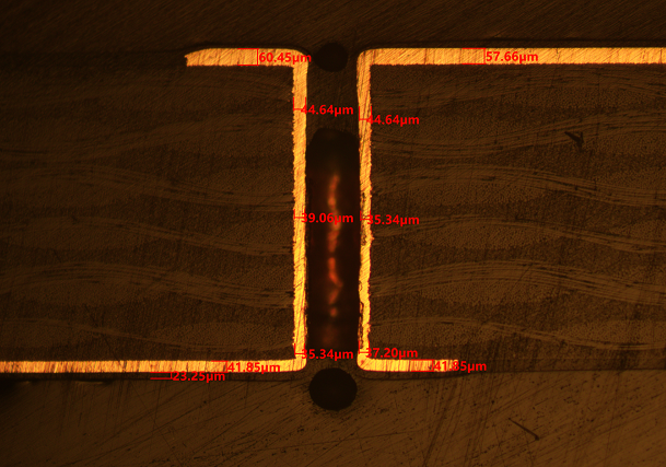
- About test coupon.
The test coupon is used to measure the characteristic impedance of the produced PCB board with TDR (Time Domain Reflectometer) to see if it meets the design requirements. Generally, the impedance to be controlled is single line and differential pair. Therefore, the trace width and line spacing (when there is a differential pair) on the test coupon should be the same as the line to be controlled. The location of the ground point during measurement is important. In order to reduce the inductance of the ground lead, the grounding point of the TDR probe is usually very close to the probe tip, so the distance and method between the point where the signal is measured on the test coupon and the ground point should be consistent with the probe used.
- In high-speed PCB design, the blank area of the signal layer can be copper-plated, and how should the copper of multiple signal layers be distributed in grounding and power supply?
Generally, the copper plating in the blank area is mostly grounded. However, when plating copper next to high-speed signal lines, pay attention to the distance between the copper plating and the signal line, because the copper plating will reduce the characteristic impedance of the trace a little. Also be careful not to affect the characteristic impedance of other layers, such as in the dual strip line structure.
- Can the signal line on the power plane be calculated using the microstrip line model? Can the signal between the power and ground planes be calculated using the stripline model?
Yes, both the power plane and the ground plane must be considered as reference planes when calculating the characteristic impedance. For example, a four-layer board: top layer-power layer-ground layer-bottom layer. At this time, the model of the characteristic impedance of the top layer routing is a microstrip line model with the power plane as the reference plane.
- Can the automatic generation of test points on high-density printed circuit boards by software generally meet the test requirements of mass production?
Whether the test points automatically generated by general software meet the test requirements depends on whether the specifications for adding test points meet the requirements of the test equipment. In addition, if the routing is too dense and the specifications for adding test points are strict, it may not be possible to automatically add test points to each line. Of course, the places to be tested need to be filled manually.
- Will adding test points affect the quality of high-speed signals?
As for whether it will affect the signal quality, it depends on the way of adding test points and how fast the signal is. Basically, the additional test point (without using the existing via or DIP pin as the test point) may be added to the line or a short line may be pulled out from the line. The former is equivalent to adding a very small capacitor to the line, and the latter is an additional branch. Both situations will have some impact on the high-speed signal, and the degree of impact is related to the frequency speed of the signal and the edge rate of the signal. The magnitude of the impact can be known through simulation. In principle, the smaller the test point, the better (of course, it must meet the requirements of the test equipment) and the shorter the branch, the better.
- How should the ground wires between the boards of a system be connected when several PCBs are connected to each other?
When the signals or power supplies between the PCB boards are in operation, for example, when the power supply or signal from board A is sent to board B, there will be an equal amount of current flowing back from the ground layer to board A (this is Kirchoff current law). The current on the ground layer will flow back to the impedance. Therefore, at each interface where the power supply or signal is connected to each other, the number of pins allocated to the ground layer should not be too small to reduce the impedance, so as to reduce the noise on the ground layer. In addition, the entire current loop can be analyzed, especially the part with larger current, and the connection method of the ground layer or ground wire can be adjusted to control the flow of current (for example, create low impedance at a certain place to let most of the current flow through this place) to reduce the impact on other more sensitive signals.