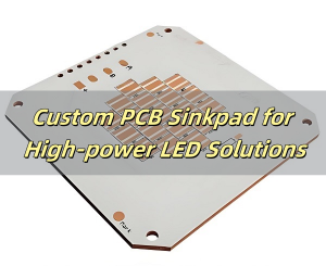
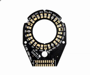
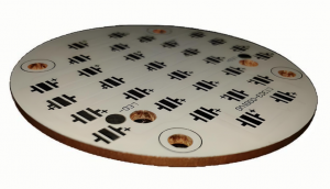
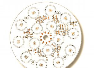
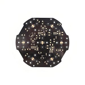
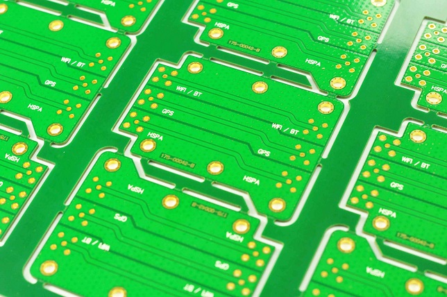
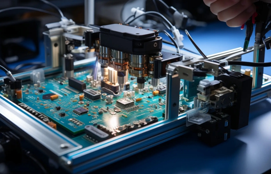
What is Aluminum Nitride PCB?
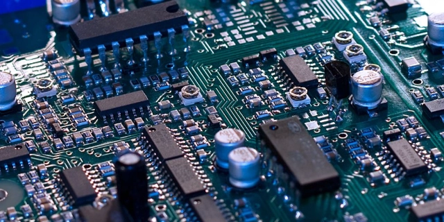
Aluminum nitride PCB also known as Aluminum nitride ceramic PCB or short for AlN PCB. It is a high-performance circuit board made from aluminum nitride ceramic, a material known for its exceptional thermal conductivity and electrical insulation properties. These boards are commonly used in industries where efficient heat dissipation is crucial, such as in power electronics, LED applications, and high-frequency devices. AlN PCBs are gaining popularity due to their ability to withstand extreme temperatures.
Benefits of AlN PCBs
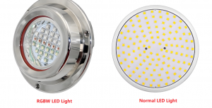
One of the key advantages of AlN PCBs is their excellent thermal conductivity, which helps prevent overheating in electronic components. With exceptional thermal conductivity of 170 W/mK, strong dielectric strength, and a low thermal expansion coefficient (CTE <4 ppm/°C), AlN is widely used in applications like high-power LEDs, lasers, high-current switches, and even ultra-low temperature vacuum electronics such as those in quantum computing. In addition to these features, AlN offers the same benefits as other ceramic materials, including rigidity, environmental and chemical resistance, and 0% water absorption.
Key reasons for choosing Aluminum Nitride over other PCB materials include:
- Outstanding thermal conductivity of 170 W/mK
- Excellent dielectric properties
- High operating temperatures exceeding 350°C
- Low thermal expansion coefficient (<4 ppm/°C)
- Compact designs due to better integration
- Hermetically sealed packages with 0% water absorption
- Minimal to no outgassing
What is the Thermal Conductivity of Aluminum Nitride PCB?
The thermal conductivity of aluminum nitride PCB ranges from 170-230W/(m·K).
The high thermal conductivity of aluminum nitride PCB is due to its unique structure and chemical composition. The thermal conductivity of aluminum nitride ceramic substrate is 2-3 times higher than that of traditional alumina ceramics and silicon-based ceramics, and 10-20 times higher than that of titanium substrate. This high thermal conductivity allows them to effectively dissipate heat from high-power electronic components, preventing overheating and ensuring stable performance. The ability to manage heat efficiently makes AlN PCBs an ideal choice for applications that generate a significant amount of heat, such as power modules, LEDs, and RF components. In comparison to other materials like aluminum oxide, which has lower thermal conductivity (around 20-30 W/mK), aluminum nitride stands out as a top choice for heat-sensitive applications.
Factors affect thermal conductivity of AlN PCB
Although the theoretical thermal conductivity of AlN is extremely high, its performance in practical applications is limited by a number of factors, mainly including:
- Microstructure
Phonon scattering is a key mechanism for heat conduction. Grain boundaries, interfaces, second phases, and defects can all affect the mean free path of phonons, thereby influencing thermal conductivity. High-purity, low-defect single-crystal AlN has a longer phonon mean free path and higher thermal conductivity.
- Oxygen Impurity Content
AlN’s strong affinity with oxygen leads to the easy introduction of oxygen impurities, which form alumina films and lattice defects, such as aluminum vacancies. These significantly reduce the phonon mean free path, lowering thermal conductivity. When the oxygen concentration is below 0.75%, oxygen atoms primarily replace nitrogen atoms in the lattice; however, exceeding this concentration causes aluminum vacancies to disappear and results in the formation of extended defects, further affecting thermal conductivity.
- Sintering Process and Additives
By selecting appropriate sintering additives (such as Y₂O₃-Li₂O, Y₂O₃-CaC₂ composite systems), densification can be achieved at lower temperatures, while reducing the formation of oxygen impurities and second phases, effectively improving the thermal conductivity of AlN ceramics. These additives help purify grain boundaries and optimize the microstructure, facilitating more efficient phonon transmission.
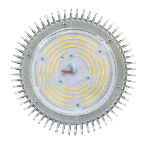
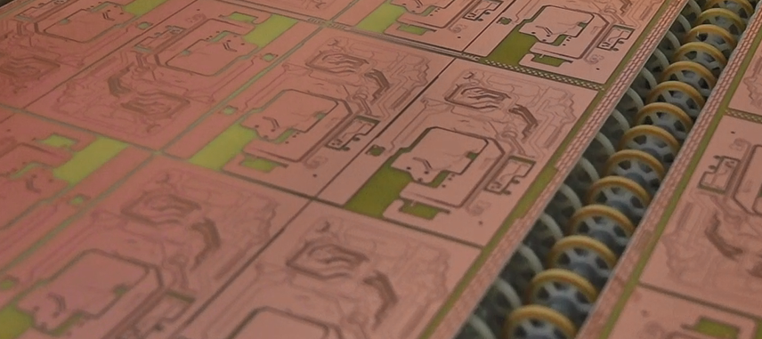
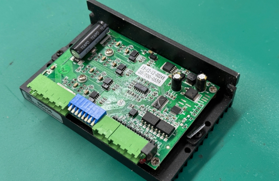
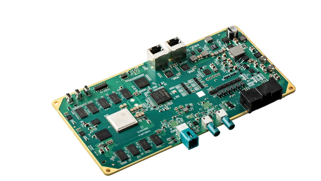
What is Aluminum Nitride PCB Used For?
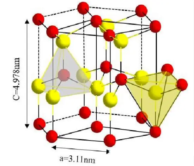
Aluminum nitride as a stable hexagonal wurtzite covalent bond compound, has shown extensive application potential in the field of electronics and optoelectronics due to its unique physical and chemical properties. Its crystal structure takes AlN4 tetrahedron as the basic unit, space group P63mc, belongs to the hexagonal crystal system, which gives AlN a series of excellent properties and use in advanced applications.
Some common applications include:
- Optical Communication
- Integrated Circuits and High-Power Electronic Devices
- Power Electronics
- Wafer chips
- Epoxy Resin Packaging
- Optical Devices and Piezoelectric Devices
- Industrial Materials
- Acoustic Devices
- Aerospace
- Military
Why is Aluminum Nitride Expensive?
The high cost of aluminum nitride PCBs stems from several factors.
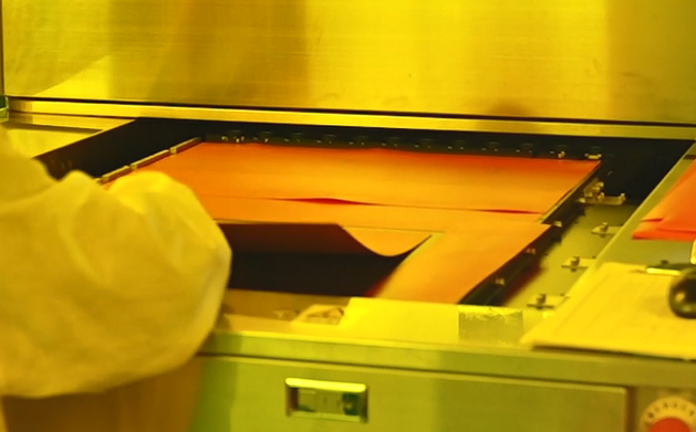
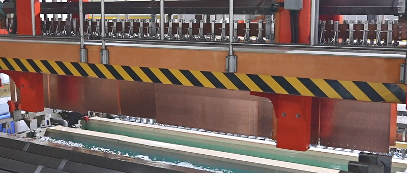
First of all, the raw material cost of aluminum nitride PCB is higher. The preparation of aluminum nitride powder requires high purity raw materials, synthesis methods include direct nitriding method, carbothermal reduction method, self-propagating high temperature synthesis and chemical vapor deposition method, etc. These methods have high requirements on equipment and technology, resulting in higher costs.
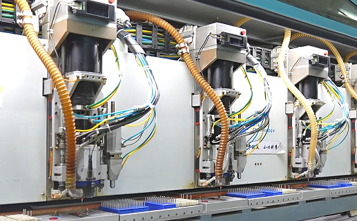
Secondly, the production process is complicated. The preparation process of aluminum nitride PCB is complex, including multiple steps such as molding and sintering, which has high requirements for equipment and technology and a high production threshold.
Finally, the market demand is large. Aluminum nitride PCB in power electronics, communication equipment, automotive electronics and other fields have a wide range of applications, especially in high power, high frequency and other occasions, its excellent heat dissipation and insulation performance can not be replaced, resulting in short supply in the market, the price of natural rising.
Aluminum Nitride PCB vs. Alumina Oxide PCB
Both aluminum nitride (AlN) and alumina oxide (Al2O3) are ceramic materials used in PCB manufacturing, but they differ significantly in terms of performance. AlN offers superior thermal conductivity, typically 170-230 W/mK, compared to aluminum oxide’s lower range of 20-30 W/mK. This makes AlN the better option for applications requiring efficient heat dissipation, such as high-power electronics and LED lighting.
However, aluminum oxide is more cost-effective and is often used in applications where high thermal conductivity is not as crucial. While Al2O3 provides good electrical insulation and is easier to produce, it may not perform as well in heat-sensitive environments as AlN. Therefore, the choice between AlN and Al2O3 depends on the specific thermal and budgetary requirements of the application. Here are the parameters of AlN and Al2O3 materials:
| Parameter | Aluminum Nitride (AlN) | Alumina Oxide (Al2O3) |
| Thermal conductivity | 170-230 W/m.k | 24-30 W/m.k |
| Dielectric constant | 8.8 | 9.2-10 |
| Dielectric strength | 15-25kV/mm | 10-15kV/mm |
| Temperature resistance | 1000-1500C | 1000-1200C |
| CTE | 4.0 ppm/K | 6.5-7 ppm/K |
| Flexural strength | 450MPa | 320MPa |
| Dielectric breakdown voltage | 14 V/m | 10 V/m |
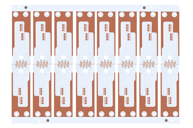
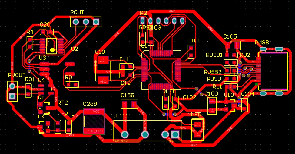
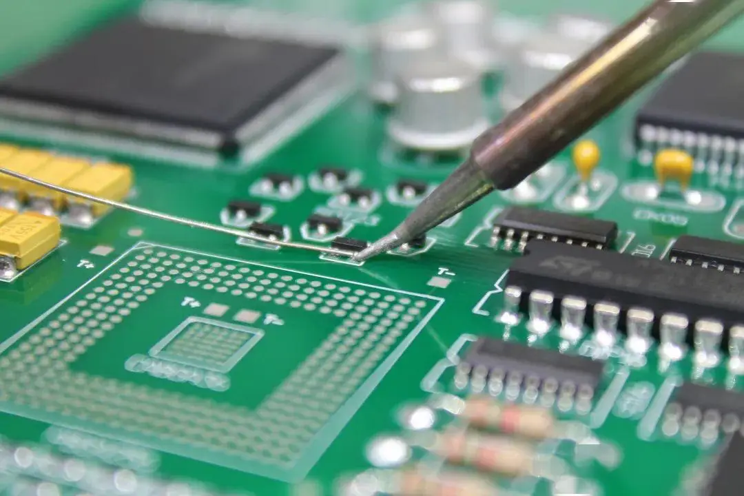
AlN Ceramic PCB Design Considerations
When designing an aluminum nitride PCB, several factors need to be considered to optimize performance:
1. Trace Width
The trace width on AlN PCBs should be a minimum of 10 mils. This ensures that the conductor cross-section is sufficient to handle the current and heat dissipation needs. Given the thermal advantages of AlN, wider traces help in spreading heat more efficiently, minimizing the risk of overheating in power-dense applications.
2. Trace Clearance
Clearances between adjacent traces should be at least 8 to 10 mils. AlN PCBs often work with higher voltage levels, making spacing critical to prevent arcing or dielectric breakdown. In high-power designs, careful spacing between traces reduces the likelihood of signal interference and maintains the board’s insulation integrity.
3. Via Pads
For via pads, a minimum diameter of 16 mils is recommended. This provides sufficient area for stable soldering and ensures proper electrical connection through the via. Depending on the board’s application, larger via pads may be necessary to accommodate higher currents or thermal dissipation needs. Via sizing should also account for assembly techniques, such as reflow soldering or thermal management features, like thermal vias, which enhance heat transfer away from components.
4. Pad Geometry Adjustments
Unlike FR-4 designs, AlN PCBs often require specific adjustments in pad geometries. The mechanical and thermal properties of AlN are quite different from those of traditional PCBs. The expansion rate, hardness, and substrate fragility mean that pad designs should allow for thermal expansion and contraction without causing stress fractures. Proper pad design also ensures better solder joint reliability, particularly for components exposed to continuous thermal cycling.
5. Gold Plating for Wire Bonding Pads
In high-performance applications, wire bonding is often used, and gold plating is a preferred surface finish for wire bonding pads. The use of gold provides a stable, corrosion-resistant surface that improves bond integrity and longevity. Wire bonding is especially critical in high-frequency, high-reliability devices, where the connections must maintain integrity under thermal stress or in harsh environments.
6. Component and Solder Matching
All components and solder materials must match the electrical and mechanical properties of the AlN substrate. Mismatches in thermal expansion between the PCB material and components can lead to stress, causing cracking or delamination. It’s important to select components and solder that can withstand high temperatures and thermal cycles while maintaining compatibility with AlN’s characteristics, especially in applications like power electronics and RF circuits.
7. Hermetic Sealing and Height Restrictions
For applications requiring hermetic sealing, such as aerospace or medical devices, height restrictions may apply to the components on the PCB. Hermetic seals protect against moisture and environmental contaminants, ensuring long-term reliability in sensitive applications. The overall component height should be kept in line with the sealing requirements, and compact designs are often necessary to meet stringent packaging constraints.
8. Thermal Expansion Management
When attaching large dies or high-power devices, it’s crucial to model and account for thermal expansion. Even though AlN has a low thermal expansion coefficient (<4 ppm/°C), the difference in expansion rates between components and the substrate can create mechanical stress, especially during thermal cycling. Careful design, including flexible connections or underfill materials, can help mitigate these effects.
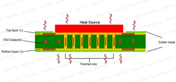
9. Thermal Vias
Thermal vias are essential for managing heat in high-power applications. By placing thermal vias directly underneath hot components, heat can be efficiently transferred away from sensitive areas, extending the lifespan of both the components and the PCB itself. In many designs, a network of thermal vias is integrated with heat sinks or spreaders to further improve heat dissipation.
10. Surface Finishes and Coatings
Aluminum nitride PCBs can benefit from surface finishes such as electroless nickel immersion gold (ENIG) or immersion silver, which protect the copper traces from oxidation and provide excellent solderability. The choice of surface finish may also depend on the specific application environment and the reliability requirements, especially in high-power or high-frequency circuits.
FAQs About AlN PCBs
1. How durable are aluminum nitride PCBs?
AlN PCBs are highly durable and can withstand extreme temperatures and harsh environments.
2. Can AlN PCBs be used in high-frequency applications?
Yes, aluminum nitride PCBs are well-suited for high-frequency and high-speed applications due to their excellent electrical insulation and low signal loss.
3. Are aluminum nitride PCBs environmentally friendly?
While the production process can be resource-intensive, AlN PCBs offer longer lifespans and higher efficiency, which can reduce the environmental impact over time.
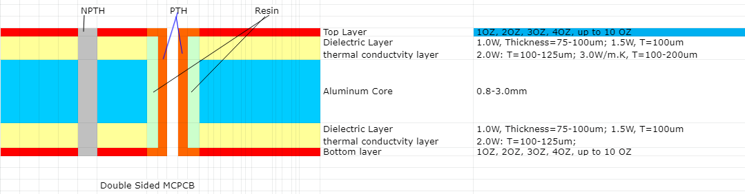
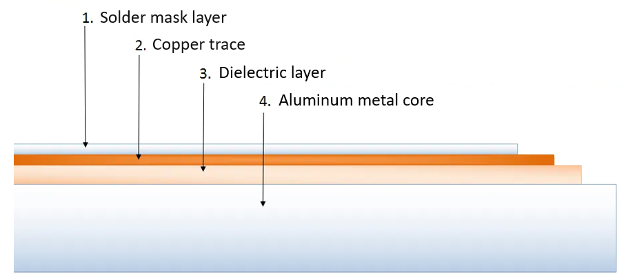
4. How do AlN PCBs compare with metal-core PCBs?
Metal-core PCBs, such as those with an aluminum core, provide good thermal management but lack the superior electrical insulation of AlN PCBs. AlN PCBs are preferred for applications requiring both high thermal conductivity and insulation.
5. What industries typically use aluminum nitride PCBs?
Industries like power electronics, aerospace, automotive, and telecommunications commonly use AlN PCBs for their high-performance needs.