If you’ve worked on PCB design, especially high-density layouts, you’ve probably wondered: what exactly is via in pad, and when should you use this technology instead of traditional routing methods? Via in pad is a critical technique for modern electronics, but it’s often misunderstood, leading to costly mistakes or missed opportunities to optimize your board. This guide breaks down everything you need to know about via in pad, from its definition and benefits to design rules and common pitfalls, all in simple, actionable terms.
What is Via in Pad?
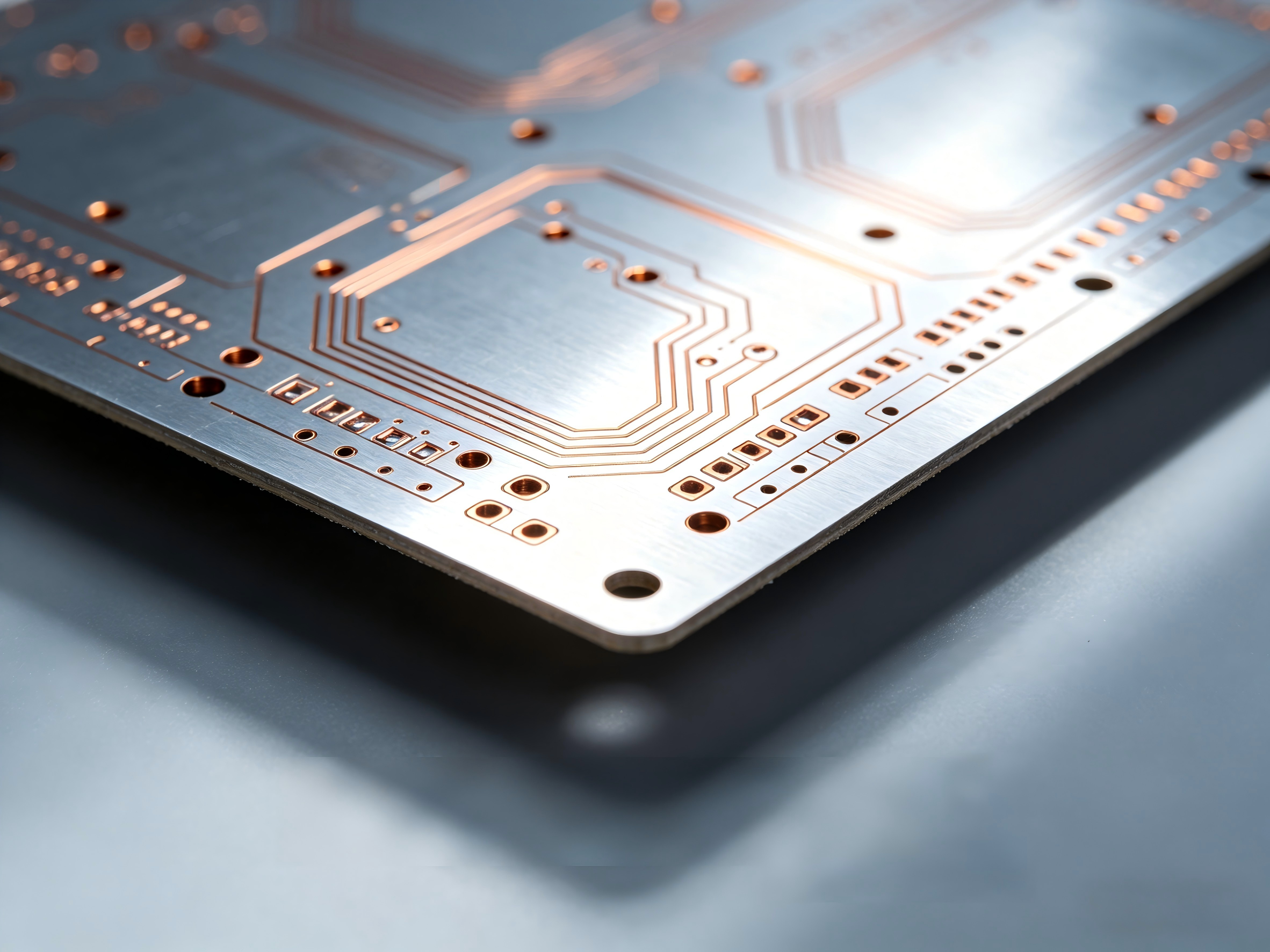
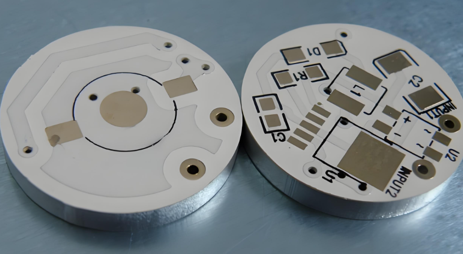
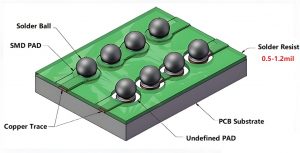
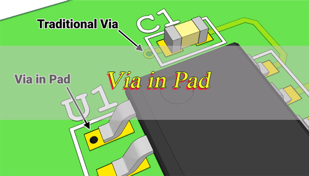
Via in pad is a PCB design technique where a via is placed directly within the copper landing pad of a surface mount component, rather than routing a trace away from the pad to a separate via location. Unlike traditional vias that sit adjacent to pads, via in pad integrates the via and pad into a single structure, eliminating the small trace stub that typically connects a pad to a nearby via.
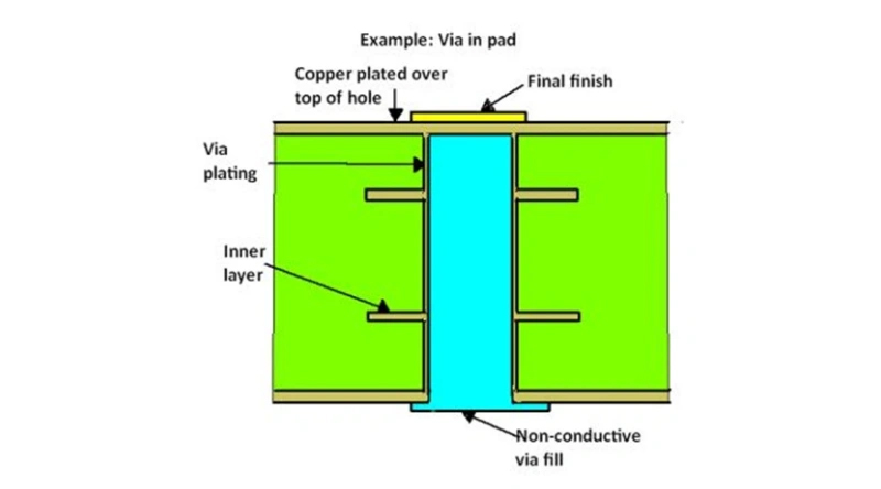
To function properly, via in pad requires specialized manufacturing steps: the via is drilled directly into the component pad, plated with copper to establish a conductive path, filled with epoxy resin or copper paste to stabilize the hole, and then planarized or capped with copper to create a smooth, solderable surface.
This process ensures the pad remains flat for component mounting and prevents solder from wicking into the via during assembly. We will also touch on related terms like in pad via and pad in via, which refer to the same core concept but with slight phrasing variations, as well as pcb via in pad which specifies the application on printed circuit boards.
Why Use Via in Pad Technology?
The primary reason to use via in pad is to solve space and performance challenges in high-density PCB designs. Here are the key benefits, explained clearly:
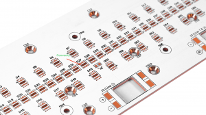
Space Optimization: Modern electronic devices like smartphones, wearables, and medical implants demand smaller PCBs with more components. Via in pad eliminates the need for fanout traces (the small lines connecting pads to adjacent vias), reclaiming valuable board space. This is critical for high density interconnect PCBs where every square millimeter counts.
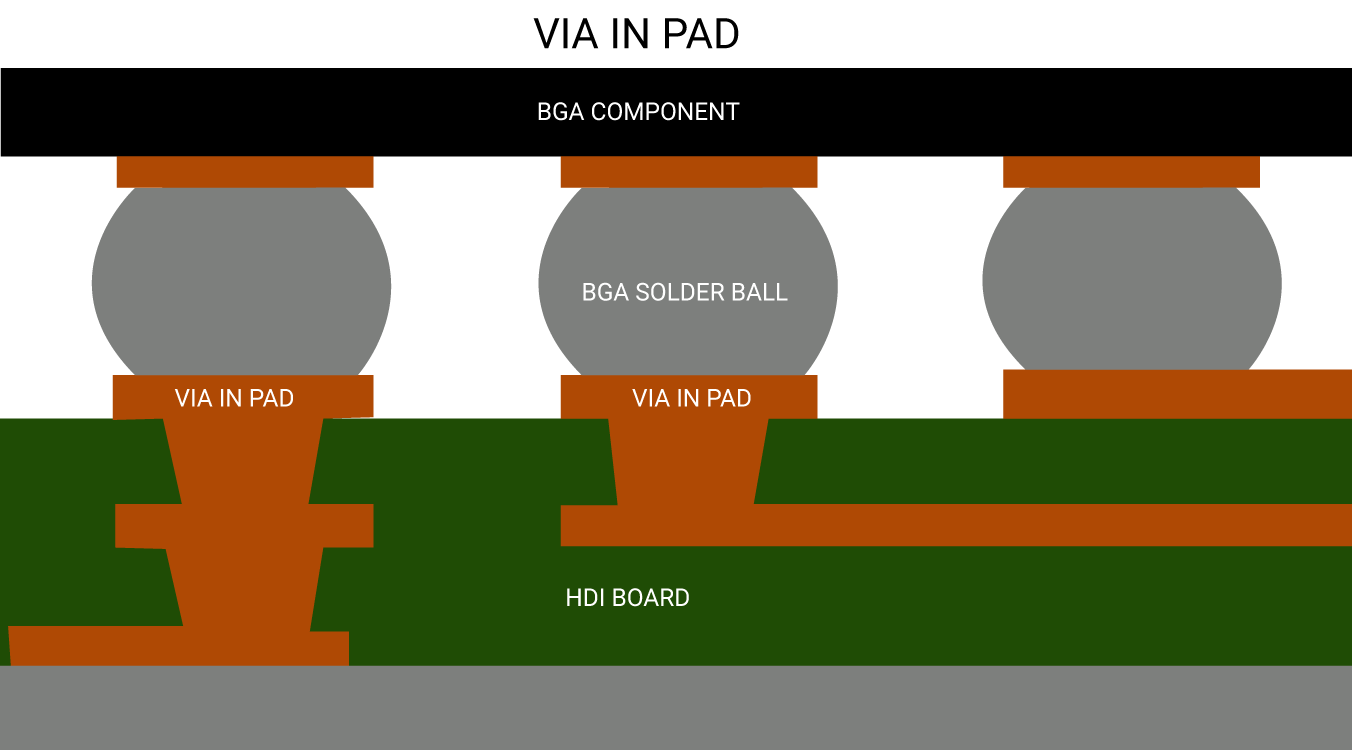
Improved Signal Integrity: Via in pad shortens the signal path, reducing parasitic inductance and capacitance that degrade signal quality. This is essential for high-speed signals (32 Gbps and beyond), as it minimizes impedance mismatches, reflections, and crosstalk. For example, via in pad bga designs (where vias are placed in BGA component pads) significantly improve signal performance for fine-pitch BGA packages.
Enhanced Thermal Management: Vias in pads act as heat conductors, transferring heat from high-power components (like power ICs or RF modules) to inner or bottom PCB layers. This prevents overheating and improves component reliability, especially in compact devices with limited airflow.
Support for Fine-Pitch Components: When BGA ball pitch drops below 0.5 mm, there is not enough space between pads for traditional dog bone routing. Via in pad is the only practical solution for these tight-pitch packages, allowing for proper fanout without sacrificing space or performance.
Does Via in Pad Make a Pad Stronger?
No, via in pad does not make a pad stronger. In fact, the drilled hole within the pad slightly reduces the pad’s structural integrity. The via creates a small opening in the copper pad, which can act as a stress concentration point during thermal cycling or mechanical stress (like component insertion or board flexing).
However, the filling and planarization process used in via in pad manufacturing helps mitigate this weakness. Epoxy or copper filling reinforces the via, preventing the pad from cracking around the hole.
When done correctly, via in pad maintains adequate mechanical strength for most applications, but it should never be considered a way to strengthen padsits benefits are focused on space and performance, not structural rigidity.
Why not Via in Pad?
While via in pad offers significant advantages, it is not suitable for every design. Here are the main reasons to avoid via in pad:
Assembly Risks (Without Proper Processing): Unfilled or improperly capped vias in pads cause solder wicking molten solder flows into the via during reflow, leaving insufficient solder on the pad. This leads to cold joints, poor solder connections, or solder voids, all of which compromise connection reliability. Even small gaps in the via cap can trap air or flux, creating bubbles in the solder joint.
Manufacturing Complexity: Via in pad requires additional steps compared to traditional vias, including precise drilling, filling, planarization, and capping. These steps increase the risk of manufacturing errors, especially if your PCB manufacturer lacks experience with the technology.
Overkill for Simple Designs: If your PCB has large component pitches (0.8 mm or larger) and ample routing space, via in pad is unnecessary. Traditional dog bone routing is simpler, cheaper, and more reliable for low-density or low-speed designs.
Repair Difficulties: Components soldered to via in pad are harder to rework. The filled via can absorb heat during desoldering, making it harder to remove the component without damaging the pad or PCB.
Why is Via in Pad Expensive?
Via in pad is more expensive than traditional via routing because of its complex manufacturing process. Here’s a breakdown of the cost drivers:
Additional Manufacturing Steps: Unlike traditional vias, which only require drilling and plating, via in pad needs filling (with epoxy or copper), planarization (to smooth the pad surface), and cap plating (to create a solderable finish). Each of these steps adds labor, time, and material costs.
Precision Requirements: Via in pad requires tighter tolerances for drilling and placement. The via must be centered in the pad to avoid reducing the pad’s effective area, and the filling must be uniform to prevent surface irregularities. This precision increases manufacturing costs.
Specialized Materials: The epoxy or copper used to fill vias must meet strict electrical and thermal requirements. These materials are more expensive than the standard materials used for traditional vias.
Quality Control: Extra inspection steps are needed to ensure via filling, planarization, and capping are done correctly. This adds to the overall cost, as manufacturers must invest in additional testing equipment and labor.
How Much Does Via in Pad Cost?
The cost of via in pad varies based on several factors, including PCB size, layer count, via quantity, filling material, and manufacturer capabilities. As a general guideline, via in pad adds 15 to 25 percent to the total PCB manufacturing cost compared to traditional via routing.
For example, a 4-layer HDI PCB with 100 via in pad features might cost $1.50 to $2.50 per via in addition to the base PCB cost. Copper-filled vias are more expensive than epoxy-filled ones, adding an extra 5 to 10 percent per via. The cost per via decreases slightly for high-volume orders, but it still remains higher than traditional vias.
When budgeting for via in pad, factor in not just the direct manufacturing costs but also potential savings from reduced PCB size, improved performance, and fewer design iterations.
What is the Difference between Via-in-Pad and Dog Bone?
Via-in-pad and dog bone (traditional via routing) are two methods for connecting component pads to inner PCB layers. The key differences are outlined in the table below, with clear comparisons to help you choose the right method for your design:
| Feature | Via-in-Pad | Dog Bone |
|---|---|---|
| Via Location | Directly within the component pad | Adjacent to the pad, connected by a fanout trace |
| Space Requirement | Minimalno space needed for fanout traces | Requires space for fanout trace plus via |
| Manufacturing Process | Requires filling, planarization, and cap plating | Standard drilling and plating (no extra steps) |
| Cost | 15–25% higher than dog bone | Lower, more cost-effective |
| Signal Integrity | Superiorshorter signal path, less parasitic interference | Inferiorlonger signal path, more parasitic inductance/capacitance |
| Best For | Fine-pitch BGA (≤0.5 mm), HDI PCBs, high-speed signals | Large-pitch components (≥0.8 mm), low-density designs, low-speed signals |
| Thermal Performance | Enhancedvias transfer heat directly from the pad | Limitedheat transfer depends on trace width |
Is Via in Pad Allowed?
Yes, via in pad is allowed in most PCB designs, but it is subject to specific manufacturing and design constraints. The key factor is whether your PCB manufacturer can support the technologysome smaller manufacturers may lack the equipment or expertise for filling, planarization, and cap plating.
Additionally, certain industry standards (like IPC-6012 for rigid PCBs) outline requirements for via in pad, including filling material, planarization tolerance, and pad integrity. As long as your design meets these standards and your manufacturer can comply, via in pad is fully allowed.
For military, aerospace, or medical applications, via in pad may require additional testing and documentation to ensure reliability. Always confirm with your manufacturer and review relevant standards before incorporating via in pad into critical designs.
What are the Via in Pad Design Rules?
Following proper design rules is critical to ensure via in pad works reliably. Below are the key rules, organized for clarity and ease of implementation:
1. Via Size and Placement: The via should be centered in the pad to maximize the remaining copper area. A good rule of thumb is to keep the via diameter 50 to 70 percent of the pad diameter. For example, a 0.8 mm pad should use a 0.4 to 0.56 mm via. Avoid placing vias too close to the pad edgemaintain a minimum distance of 0.1 mm between the via and pad edge to prevent cracking.
2. Filling Requirements: All vias in pads must be fully filled (epoxy or copper) and capped with copper. Unfilled vias will cause solder wicking and reliability issues. Copper filling is recommended for power or ground pads, as it improves thermal and electrical conductivity; epoxy filling is suitable for signal vias.
3. Pad Size Adjustment: Increase the pad size slightly to compensate for the via. If you use a standard pad size with a via in pad, the effective copper area decreases, weakening the solder joint. A 0.1 to 0.2 mm increase in pad diameter is typically sufficient.
4. Annular Ring: Maintain a minimum annular ring (the copper around the via) of 0.1 mm. This ensures proper electrical connection and mechanical stability. If space is limited, you can reduce the annular ring to 0.05 mm, but this increases manufacturing risk.
5. Clearance: Ensure adequate clearance between via in pad and adjacent components or traces. A minimum clearance of 0.2 mm is recommended to prevent short circuits and ensure proper assembly.
6. BGA-Specific Rules: For via in pad bga designs, match the via size to the BGA ball pitch. For 0.5 mm pitch BGA, use 0.2 to 0.3 mm vias; for 0.4 mm pitch, use 0.15 to 0.25 mm vias. Avoid placing vias under BGA balls that carry high-current signals, as this can cause thermal issues.
How to Change Via Pad Size in Eagle?
Changing via pad size in Eagle is a straightforward process, but it requires adjusting both the via definition and design rules to ensure compatibility. Follow these step-by-step instructions:
1. Open the Via Library: Launch Eagle and open your PCB design. Go to the “Library” menu and select “Open Library Manager.” Find the via library you are using (typically “via.lbr”) and open it.
2. Edit the Via: In the library editor, select the via you want to modify (e.g., “VIA1”). Right-click and choose “Edit.” A new window will open showing the via’s properties, including pad diameter and hole size.
3. Adjust Pad and Hole Size: Change the “Pad Diameter” to your desired size (e.g., from 0.6 mm to 0.7 mm). Adjust the “Hole Size” accordinglyremember to maintain a proper annular ring (minimum 0.1 mm). For example, if you set the pad diameter to 0.7 mm, the hole size should not exceed 0.5 mm.
4. Save the Changes: Click “OK” to save the modified via. Close the library editor and return to your PCB design.
5. Update the Design Rules: Go to the “Design” menu and select “Design Rules.” Navigate to the “Routing” tab and find the “Via Size” rule. Update the rule to match your new via pad and hole size. This ensures Eagle checks for proper clearance and annular ring during design rule checks (DRC).
6. Run DRC: After making changes, run a DRC to identify any issues (e.g., insufficient clearance, incorrect annular ring). Fix any errors before finalizing your design.
FAQs About Via-in-PCB
Q1: Can via in pad be used for power and ground pads?
A1: Yes, via in pad is ideal for power and ground pads. Copper-filled vias in these pads improve thermal conductivity, helping to dissipate heat from high-power components. They also provide a direct, low-resistance path between layers, reducing voltage drop.
Q2: Do all PCB manufacturers support via in pad?
A2: No, not all manufacturers support via in pad. Smaller manufacturers may lack the equipment for filling, planarization, and cap plating. Always confirm with your manufacturer before designing with via in pad, and ask for samples of their previous via in pad work to verify quality.
Q3: Is via in pad necessary for HDI PCBs?
A3: While not always necessary, via in pad is highly recommended for HDI PCBs. HDI designs require high component density and small form factors, and via in pad eliminates the need for fanout traces, maximizing board space and improving signal performance.
Q4: Can I use via in pad with 0201 or 01005 components?
A4: It is possible, but not recommended. These ultra-small components have very small pads, and placing a via in the pad will significantly reduce the effective copper area, weakening the solder joint. Use traditional dog bone routing for ultra-small components unless space is extremely limited.
Q5: How do I prevent solder wicking with via in pad?
A5: Solder wicking is prevented by fully filling and capping the via. Ensure your manufacturer uses high-quality filling material (epoxy or copper) and properly planarizes the pad surface. Avoid using unfilled or partially filled vias in pads, as these will almost always cause solder wicking.
Q6: Does via in pad affect signal impedance?
A6: Yes, but when designed correctly, it improves impedance control. Via in pad shortens the signal path, reducing parasitic inductance and capacitance, which helps maintain consistent impedance. Use impedance calculation tools to ensure the via and pad size match your signal requirements.