If you’re working on a PCB project, you’ve likely asked: what’s the difference between laser etching vs laser engraving, and which one is right for your PCB manufacturing needs? Whether you’re prototyping a small board or scaling up production, choosing between these two processes can make or break your project’s precision, durability, and cost-effectiveness. This guide breaks down critical details to help you make an informed decision, including depth, surface impact, material compatibility, laser type selection, and how laser marking fits into PCB traceability.
What Are the Differences Between Laser Etching VS Laser Engraving for PCB Manufacturing?
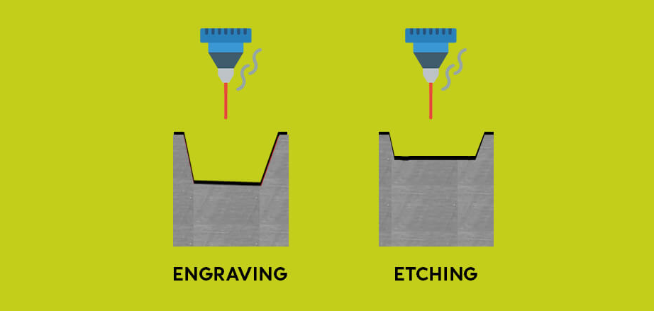
The core difference between laser etching vs laser engraving lies in how each process interacts with PCB materials. Both are used in production but serve different purposes. Below is a concise, comprehensive table comparing the two processes:
| Characteristic | Laser Etching | Laser Engraving |
| Process Mechanism | Heats surface to melt/oxidize; creates visible marks without significant material removal | Vaporizes and removes material to create deep, recessed marks |
| Primary Use | Fine trace patterns, surface marking, resist layer preparation | Deep component identifiers, thick copper removal, durable traceability marks |
| Material Impact | Minimal surface disruption; no risk of weakening PCB structure | Material removal may slightly weaken thin PCBs if uncontrolled |
| Precision Level | High precision for fine lines and tight spacing | Good precision but limited by material removal depth |
Key takeaways:
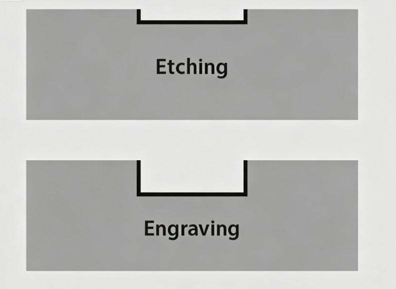
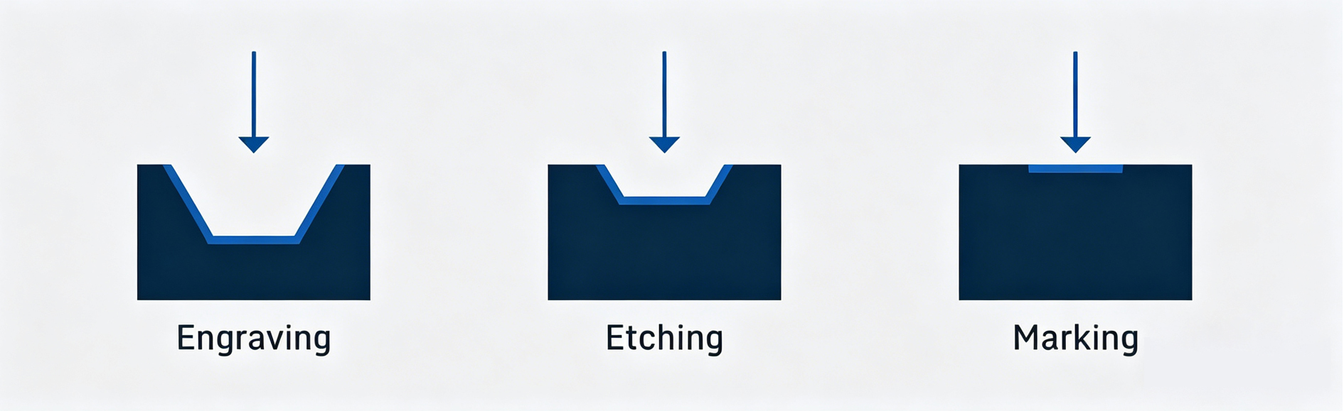
- Laser Etching: Surface modification only; ideal for precision and fine details.
- Laser Engraving: Material removal; ideal for durable, tactile marks.
How Do Laser Etching vs Laser Engraving Differ in Depth and Surface Impact?
Depth and surface impact directly affect PCB functionality and durability. Here’s a clear breakdown:
Laser Etching:
- Shallow marks (0.0001–0.001 inches), confined to the top surface.
- Smooth surface with no tactile feel; minimal structural impact.
- Ideal for PCBs with fine traces or delicate components (avoids short circuits).
Laser Engraving:
- Deeper marks (0.001–0.020 inches), depending on laser power and material.
- Tactile marks; recesses may collect dust or affect component placement.
- Requires careful design to avoid interfering with solder joints or component leads.
Prioritize etching for precision and engraving for durability.
Which Is Faster and More Cost-Effective for PCB Prototyping?
For most PCB prototyping, laser etching is faster and more cost-effective. Below is a concise comparison:
| Factor | Laser Etching | Laser Engraving |
| Processing Speed | Fast (2–5 minutes per board) | Slower (5–15 minutes per board) |
| Energy Consumption | Low (less laser power) | High (more power to vaporize material) |
| Post-Processing | Minimal (no smoothing needed) | Moderate (may need edge smoothing) |
| Cost per Prototype | Lower (less energy, less equipment wear) | Higher (more energy, longer processing) |
Exception: Laser engraving is worth the extra time/cost for industrial PCBs needing deep, durable marks for harsh environments. For most hobbyists and engineers, etching is better.
How Do Laser Etching vs Laser Engraving Perform on Different PCB Materials?
Laser etching and engraving perform differently on common PCB materials. Below is a concise breakdown:
| PCB Material | Laser Etching Performance | Laser Engraving Performance |
| FR4 (Standard Substrate) | High contrast, no structural damage, fast processing | Deep marks, risk of fiberglass damage at high power, slower processing |
| Copper Clad Boards | Precise copper removal for fine traces, minimal oxidation | Efficient thick copper removal, risk of oxidation, higher power needed |
What’s the Difference Between Laser Marking vs Engraving vs Etching for PCB Traceability?
All three processes support PCB traceability but serve different needs. Below is a clear comparison:
| Process Type | Mechanism | Mark Durability | Ideal Use Scenarios |
| Laser Marking | Surface-level color/texture change; no material removal (barcodes, QR codes) | Moderate (prone to wear in harsh conditions) | High-volume production, consumer electronics |
| Laser Etching | Surface modification; minimal material removal | Balanced (resistant to occasional handling) | Frequent handling, mid-range traceability needs |
| Laser Engraving | Deep material removal; tactile recessed marks | Maximum (resistant to wear, chemicals, harsh environments) | Industrial, automotive, aerospace PCBs |
When to Choose Laser Etching for Fine PCB Trace Patterns?
Choose laser etching over engraving for fine PCB trace patterns when precision and minimal material impact are critical. Key reasons:
- Ultra-high precision: Achieves trace widths as small as 25 microns, meeting HDI PCB standards (≤100μm lines/spaces) and supporting compact, high-density designs.
- Smooth trace edges: No material removal, avoiding burrs or irregularities that disrupt signal flow and reduce short circuit risks, critical for high-frequency/low-voltage PCBs.
- Preserves PCB integrity: Shallow surface modification (0.0001–0.001 inches) won’t weaken the board or cause trace failure from stress points.
- Ideal for specific applications: Perfect for HDI PCBs and modern electronics (smartphones, wearables, medical devices) where space and signal integrity are key.
- Minimal oxidation risk: Gentle surface modification reduces copper oxidation, protecting trace conductivity and extending the PCB’s service life, especially when paired with surface treatments like immersion gold.
- Cost-efficient for small batches: Eliminates the need for physical masks or films, allowing quick design adjustments and lower costs for prototypes or small-volume production.
- High marking clarity: Creates crisp, legible marks that remain readable even under microscope inspection or automated scanners, improving traceability efficiency.
- Compatible with solder mask processing: Precisely defines solder mask openings without damaging the underlying substrate, ensuring reliable solder joint formation during assembly.
- Environmentally friendlier: Reduces reliance on harsh chemicals compared to traditional wet etching, minimizing waste and simplifying post-processing cleanup.
- Consistent results: Automated laser control ensures uniform trace quality across all PCBs, reducing production errors and improving batch consistency.
Can Laser Engraving Replace Laser Etching for High-Durability Marks?
Laser engraving can replace laser etching for high-durability marks in most cases, but it is not a universal substitute and has key limitations that must be considered for PCB performance.
Engraving is ideal for replacing etching when durability is the top priority, especially for industrial, automotive, or aerospace PCBs. It vaporizes material to create deep, abrasion-resistant marks that withstand harsh environments, making it the preferred choice for long-lasting traceability where durability is non-negotiable.
However, engraving cannot replace etching for precision-focused scenarios. It creates edge irregularities that disrupt signal flow, is slower and more costly, and weakens thin or flexible PCBs. For HDI PCBs, compact electronics, or delicate components, etching remains superior as its shallow modification preserves structure and signal integrity.
Common Mistakes When Choosing Between Laser Etching vs Laser Engraving for PCBs
Avoid these mistakes to ensure project success:
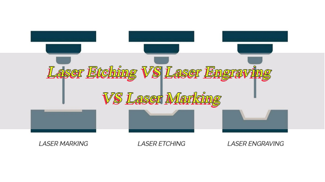
- Confusing etching and engraving: Laser etching only modifies the surface without significant material removal; laser engraving vaporizes and removes material to create deep marks.
- Overlooking material compatibility: Engraving thin FR4 can weaken the PCB structure;etching thick copper layers may not remove enough material to meet design requirements.
- Ignoring laser power settings: Too much power during etching damages the PCB substrate or causes excessive oxidation; too little power during engraving results in shallow, non-durable marks.
- Skipping test runs: Failing to test the process on scrap PCBs first often leads to costly errors in full production, especially when adjusting for new materials or designs.
- Prioritizing cost over performance: Using etching for high-durability PCBs (industrial, automotive) leads to premature mark failure; using engraving for fine-trace HDI PCBs causes signal disruption.
- Neglecting laser type compatibility: UsingCO2 lasers for copper layers (which reflect CO2 light) results in poor marks and potential equipment damage; using UV lasers for deep engraving wastes energy and time.
- Ignoring heat affect zone (HAZ) control: Failing to adjust laser parameters for HAZ can warp delicate PCB substrates, damage sensitive components, or disrupt signal integrity in high-frequency PCBs.
- Overlooking scan speed and pulse frequency matching: Mismatched speed and frequency cause uneven marks—too slow leads to over-burning, too fast results in incomplete material removal.
- Neglecting post-processing needs: Skipping edge smoothing after CO2 laser engraving on FR4 leaves burrs that interfere with component placement and solder joint formation.
- Ignoring PCB thickness when setting parameters: Using high-power lasers on thin or flexible PCBs causes structural damage; using low-power lasers onthick copper layers fails to achieve desired mark depth.
- Forgetting to calibrate laser alignment: Misaligned lasers create inaccurate marks, uneven trace edges, and inconsistent depth, leading to PCB performance issues and production waste.
- Overlooking environmental factors: Processing PCBs in dusty or humid environments contaminates laser lenses, reduces mark clarity, and increases the risk of oxidation on copper layers.
How to Select the Right Laser Type for Laser Etching vs Laser Engraving in PCB Production?
Selecting the right laser type for PCB laser etching and engraving depends on core factors like process requirements, PCB material, precision needs, production volume, and cost. Below are practical, detailed guidelines to help you make the right choice:
- Align laser type with the core process (etching vs engraving): For laser etching (surface modification, minimal material removal), prioritize lasers with low heat impact and high precision. For laser engraving (material vaporization, deep marks), choose lasers with high power and efficient material removal capabilities.
- Choose UV Lasers for high-precision laser etching: UV lasers (355nm) offer the highest precision, ideal for HDI PCBs, fine trace patterns (as small as 25 microns), and delicate components. They use cold processing to minimize heat damage, avoid copper oxidation, and ensure smooth trace edges, making them perfect for smartphones, wearables, and medical devices.
- Opt for Fiber Lasers for versatile etching and engraving: Fiber lasers (1064nm) are versatile and cost-effective for both processes. For etching, they work well with FR4 and copper clad boards, supporting high-volume production with minimal energy consumption. For engraving, they excel at copper/metal layers, creating deep marks with minimal oxidation and consistent results.
- Use CO2 Lasers for FR4-focused laser engraving: CO2 lasers (10.6μm) efficiently remove FR4 resin and fiberglass, making them ideal for engraving standard FR4 PCBs. Avoid using them for copper layers, as copper reflects CO2 laser light, leading to poor results and potential equipment damage.
- Consider PCB material compatibility: For copper layers (etching or engraving), fiber or UV lasers are preferred (resistant to copper’s high reflectivity). For FR4 substrates, CO2 lasers are efficient for engraving, while UV/fiber lasers are better for precise etching to avoid structural damage.
- Match laser power to material thickness: Thin PCBs (≤0.5mm) and fine etching require low-power lasers (5-20W) to prevent damage. Thick PCBs, thick copper layers, or deep engraving need higher power (20-150W), with CO2 lasers for FR4 and fiber lasers for copper.
- Prioritize laser type based on production volume: High-volume production benefits from fiber lasers (fast processing, low maintenance). Small batches or prototyping can use UV lasers for precision or CO2 lasers for FR4-specific engraving, balancing cost and performance.
- Account for heat impact (HAZ) control: For PCBs with sensitive components or high-frequency signals, choose UV lasers (short pulse, minimal heat affect zone) to avoid material warping or signal disruption. CO2 lasers have a larger HAZ and are better for non-sensitive FR4 engraving.
- Consider post-processing needs: UV and fiber lasers produce clean, smooth results with minimal post-processing. CO2 lasers for FR4 engraving may require light edge smoothing to remove minor carbonization, adding slight production time.
- Balance cost and performance: Fiber lasers offer the best cost-effectiveness for most PCB production. UV lasers are more expensive but necessary for ultra-precision. CO2 lasers are affordable for FR4 engraving but limited to non-copper applications.
- Test laser parameters for optimal results: Regardless of laser type, adjust power, frequency, and speed based on material and process, e.g., 5-20W UV lasers for solder mask etching, 60-150W CO2 lasers for FR4 engraving, and test on scrap PCBs first to avoid production errors.
Which Process Delivers Better Precision: Laser Etching vs Laser Engraving for HDI PCBs?
Laser etching delivers significantly better precision than laser engraving for HDI PCBs. The key reasons, broken down clearly, are as follows:
- Meets HDI PCB’s ultra-fine trace requirements: HDI PCBs typically require trace widths as small as 25 microns (≤100μm lines and spaces), and laser etching can consistently achieve this precision. Laser engraving, by contrast, is limited by material removal depth and often fails to maintain such tight tolerances.
- Creates smooth, consistent trace edges: Laser etching modifies the PCB surface without significant material removal, resulting in clean, smooth edges that avoid signal disruption. Laser engraving removes material, which frequently leaves burrs, uneven surfaces, or edge irregularities that compromise precision.
- Minimizes heat affect zone (HAZ) damage: Etching uses low-power, high-precision laser beams (especially UV lasers) with minimal HAZ, preventing material warping or damage to adjacent components. Engraving requires higher laser power, leading to a larger HAZ that distorts fine trace structures on HDI PCBs.
- Maintains tight component spacing: HDI PCBs feature dense component placement, and laser etching’s non-invasive surface modification ensures no material removal disrupts component spacing. Engraving’s recessed marks can encroach on component pads, increasing short circuit risks and reducing precision.
- Reduces copper oxidation and trace degradation: Gentle surface modification from etching minimizes copper oxidation, preserving trace conductivity and dimensional accuracy. Engraving’s material removal exposes fresh copper, increasing oxidation risk and potential trace width variations.
- Compatible with high-precision laser types for HDI: Laser etching pairs seamlessly with UV and fiber lasers—ideal for HDI PCBs—offering superior beam quality and focus. Engraving often relies on higher-power lasers (e.g., CO2) that lack the precision needed for ultra-fine HDI traces.
- Ensures consistent batch-to-batch precision: Etching’s automated, low-power process delivers uniform trace quality across all HDI PCBs, reducing production errors. Engraving’s material removal process is more prone to inconsistencies due to variations in laser power or material thickness.
- Avoids structural damage to thin HDI substrates: HDI PCBs are often thin and delicate; etching’s shallow modification preserves their structural integrity. Engraving’s material removal weakens thin substrates, leading to warping or trace failure that undermines precision.
For HDI PCBs, laser etching is the superior choice for precision due to its ability to meet ultra-fine trace requirements, create smooth edges, minimize heat damage, maintain tight component spacing, and ensure consistent, reliable results. Laser engraving, while durable, lacks the precision needed for HDI’s high-density, delicate design, as its material removal process introduces irregularities and structural risks that compromise performance. When precision is non-negotiable for HDI PCBs, laser etching is the optimal process.
FAQs About Laser Etching VS Laser Engraving
Q1: What’s the key difference between laser etching vs laser engraving?
A1:Etching modifies the surface without significant material removal (precision). Engraving vaporizes and removes material (durability).
Q2: How do they differ in depth?
A2:Etching creates shallow marks (0.0001–0.001 inches). Engraving creates deeper marks (0.001–0.020 inches).
Q3: Which is more cost-effective for prototyping?
A3:Laser etching is faster, uses less energy, and requires minimal post-processing.
Q4: How do they perform on FR4?
A4:Etching creates high-contrast, non-damaging marks. Engraving risks fiberglass damage at high power.
Q5: Can engraving replace etching for high-durability marks?
A5: Yes, but only if fine details are not required (engraving is less precise).
Q6: When to choose etching for fine traces?
A6: When precision and minimal surface impact are critical (HDI PCBs, compact electronics).
Q7: What’s the best laser type for each process?
A7: Etching: UV or fiber lasers. Engraving: Fiber or CO2 lasers (avoid CO2 for copper).
Q8: Which is more precise for HDI PCBs?
A8:Laser etching (smooth edges, no material removal disruptions).