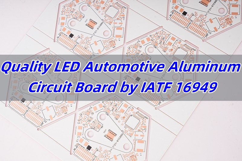
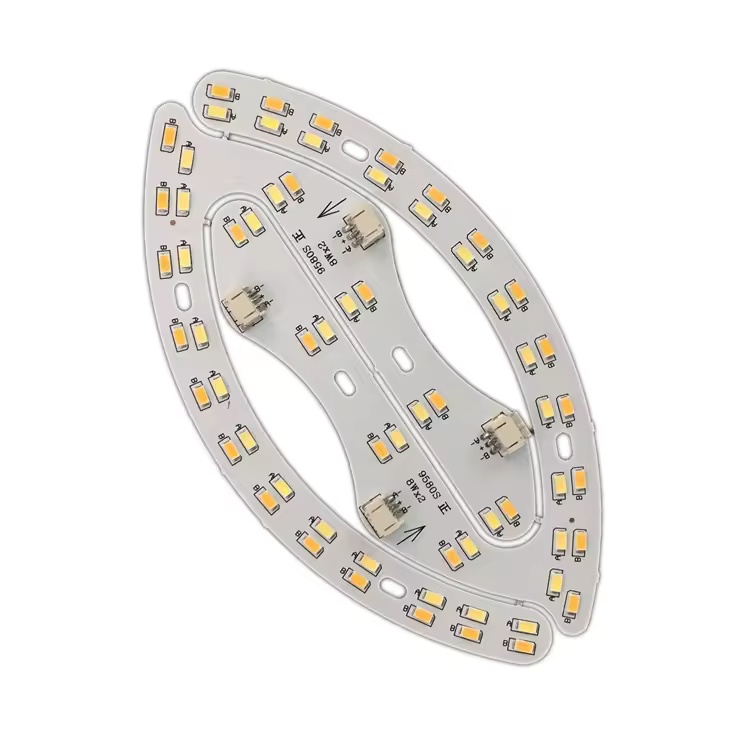
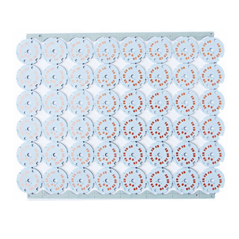
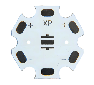
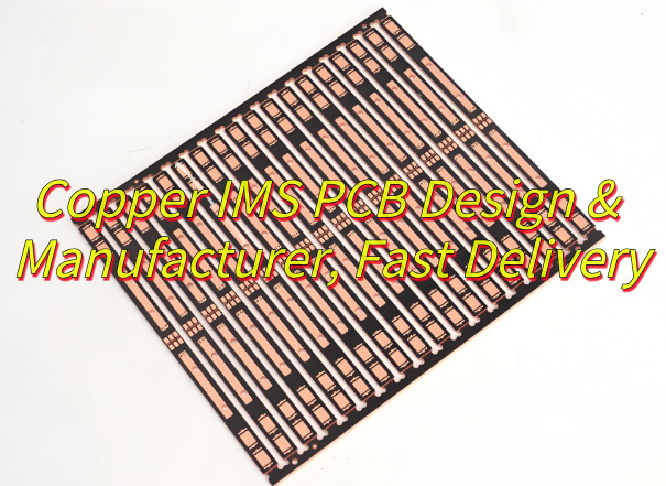
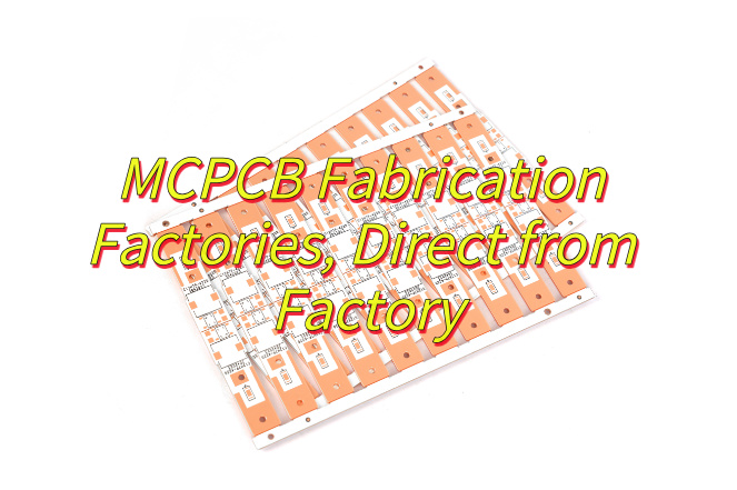
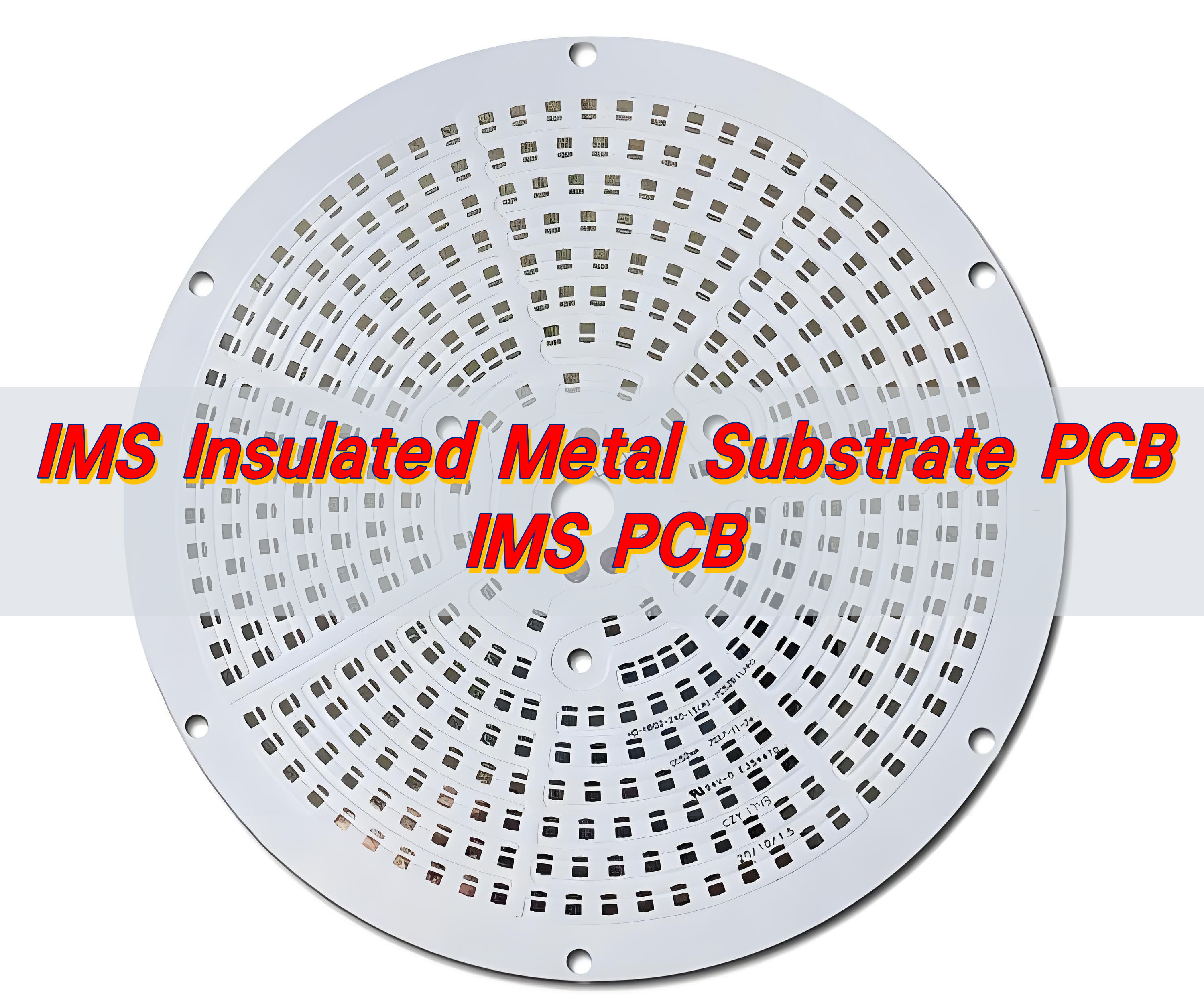
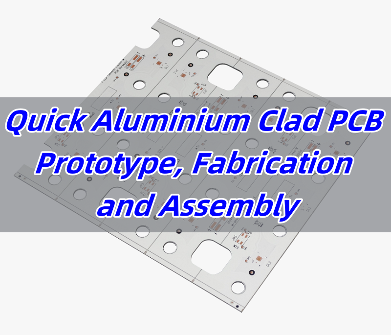
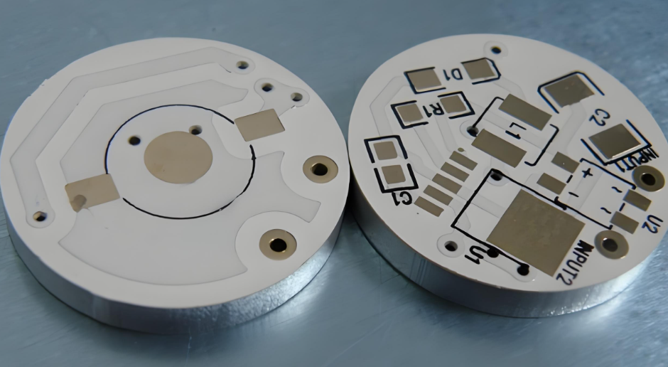
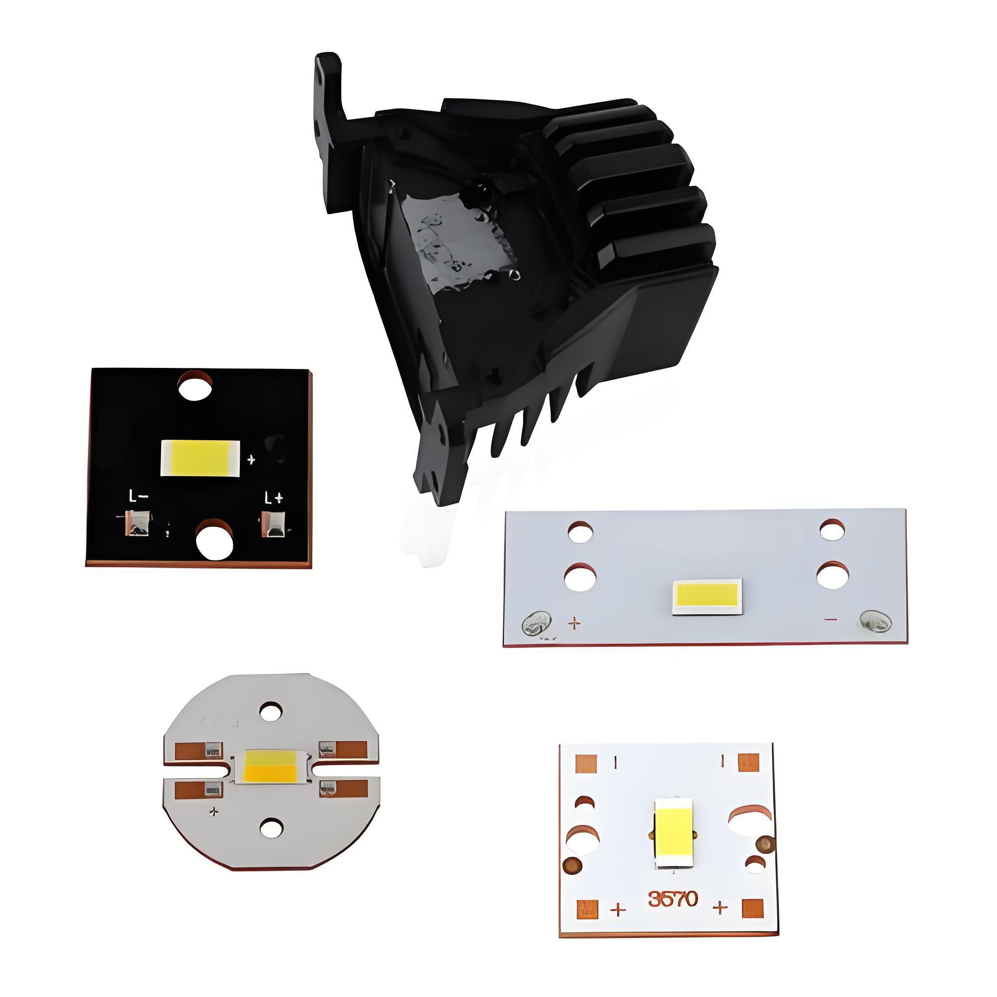
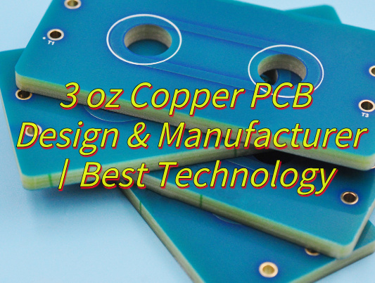
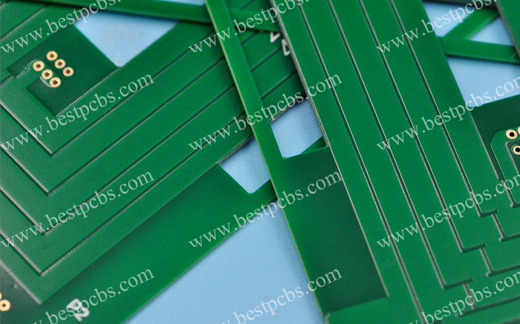
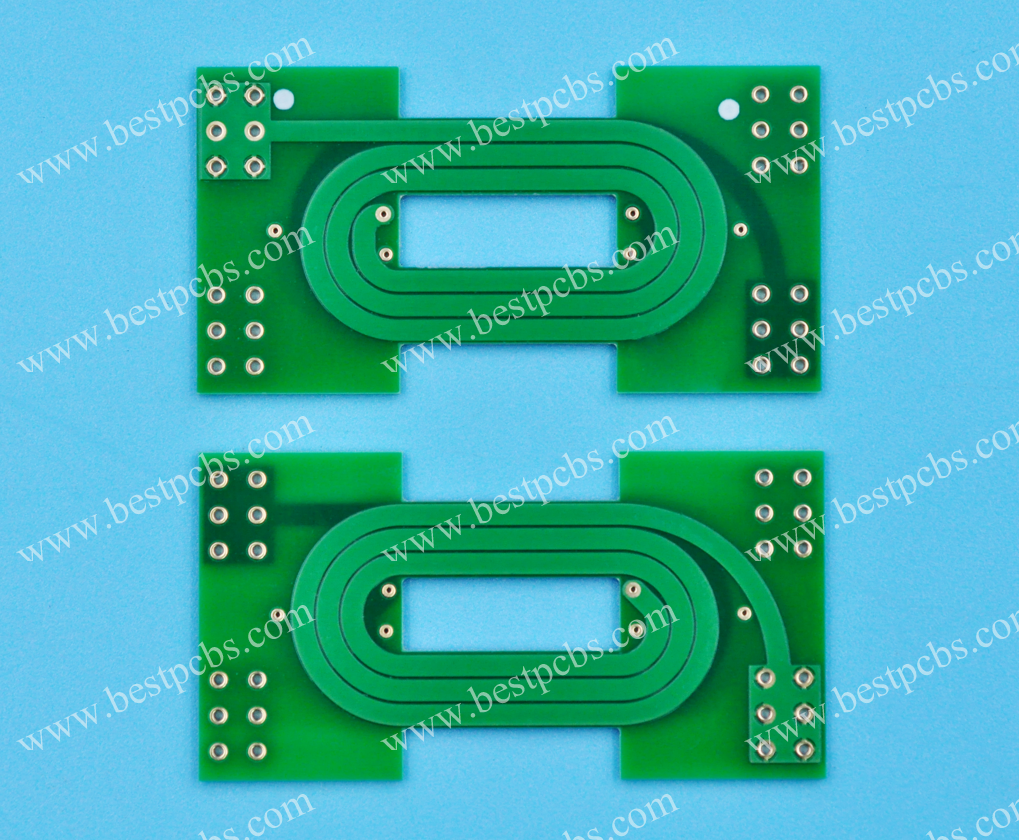
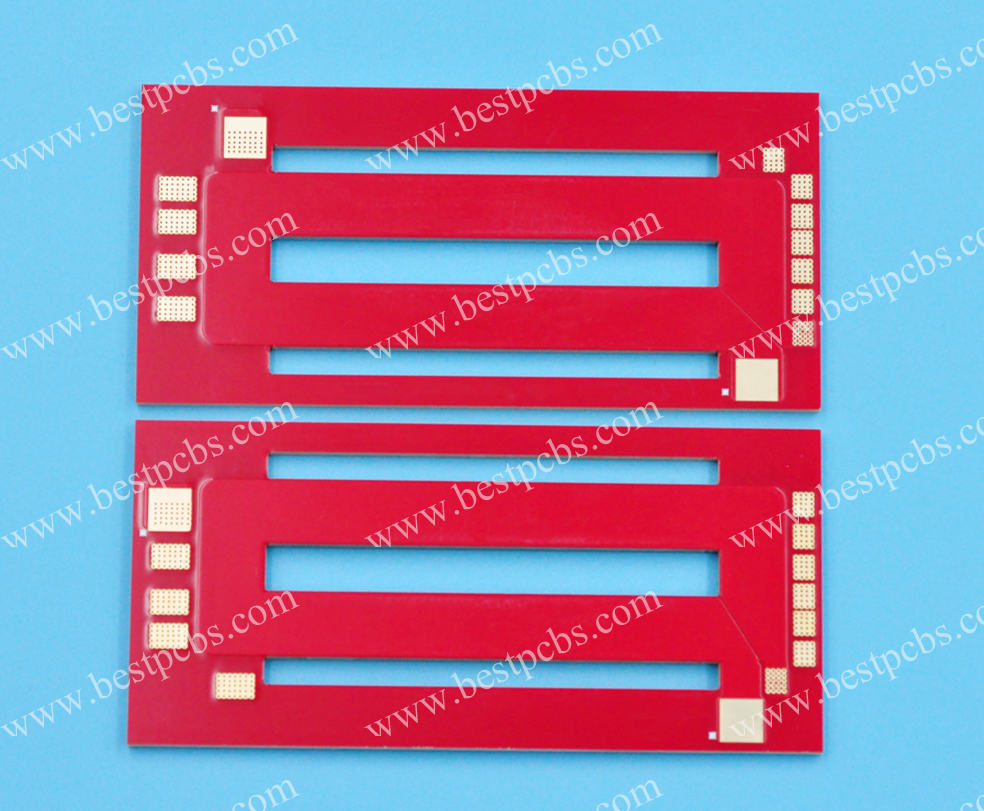
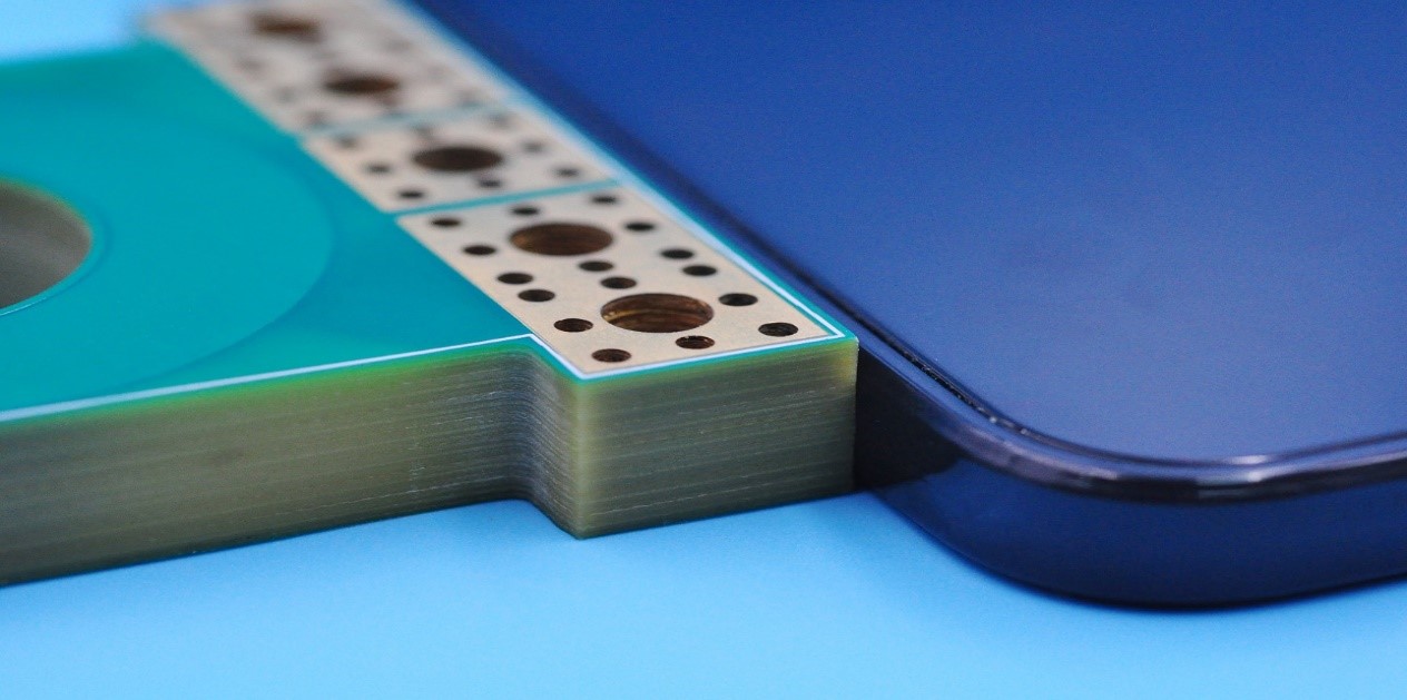
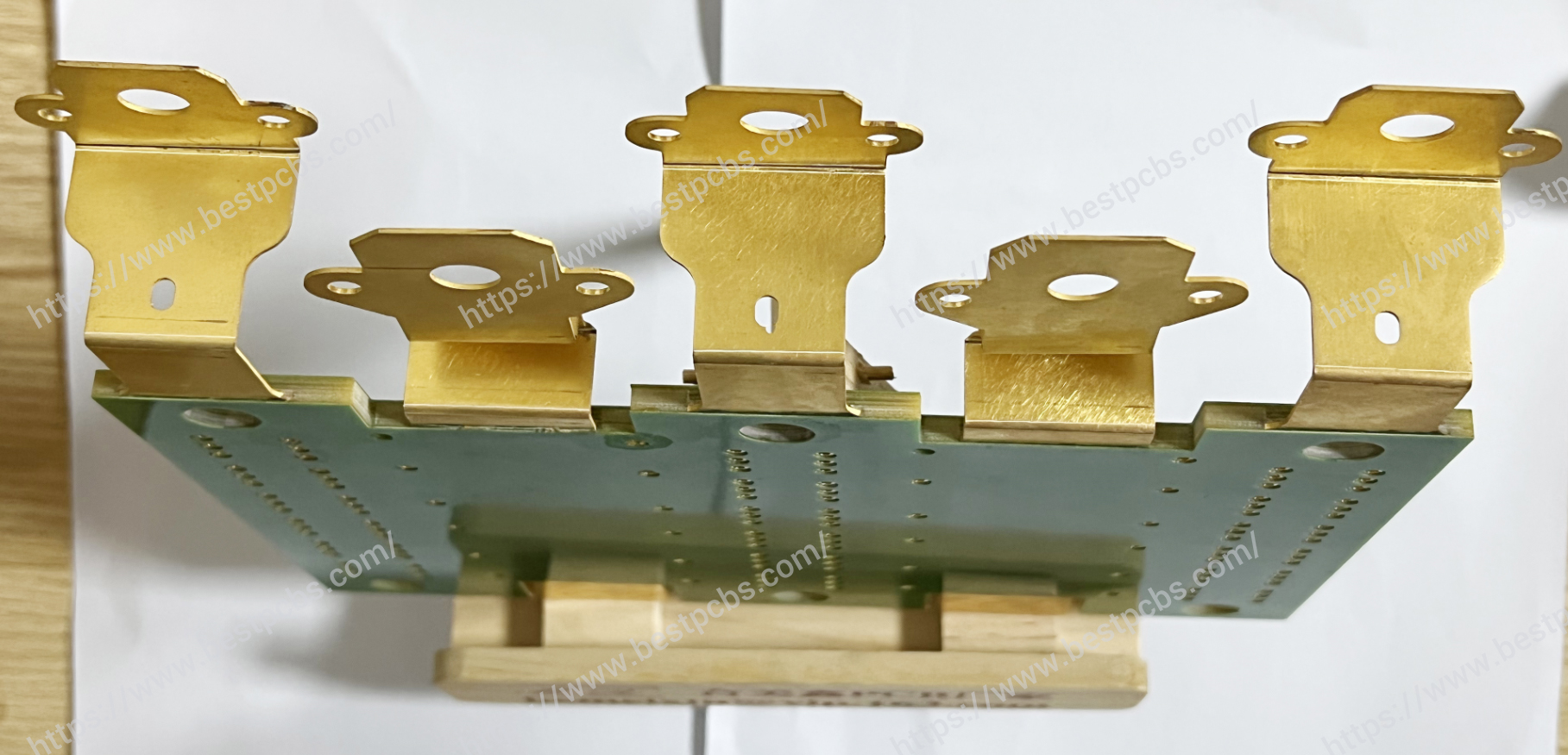
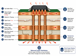
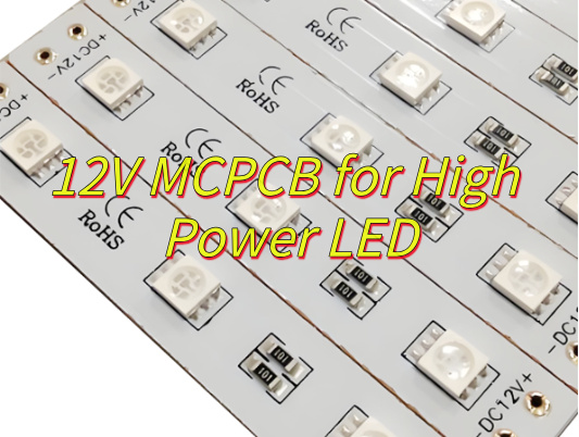
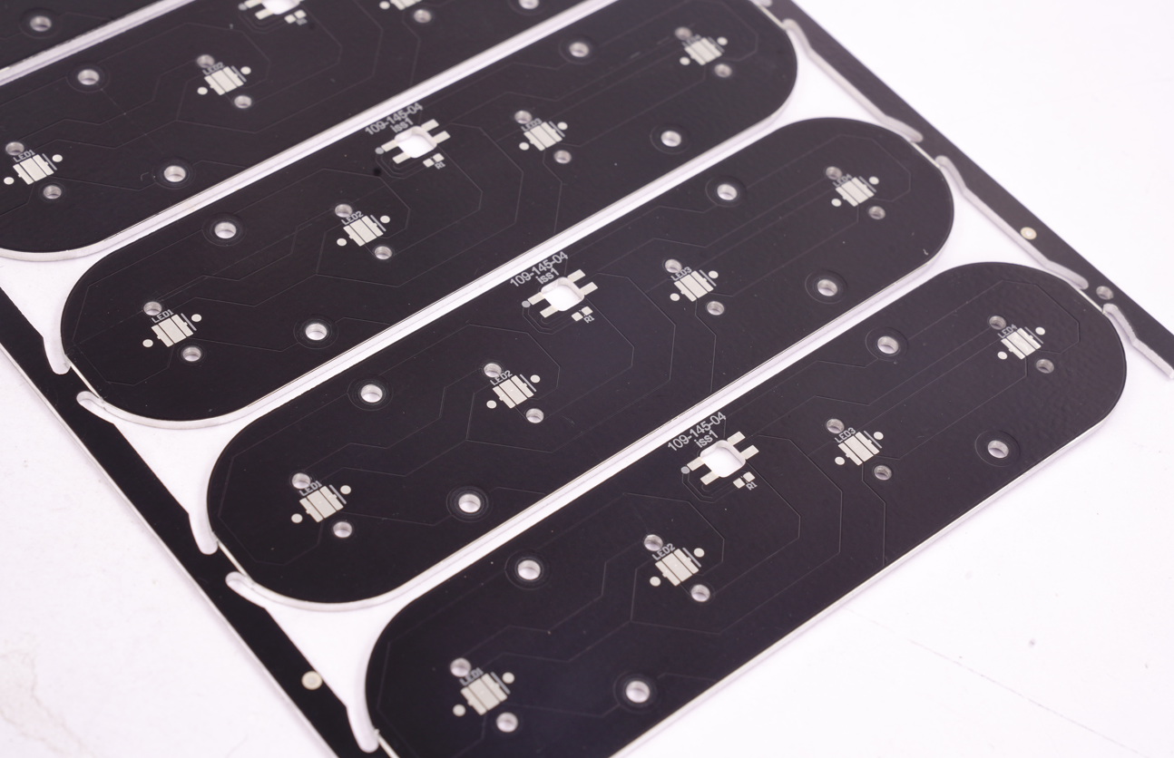
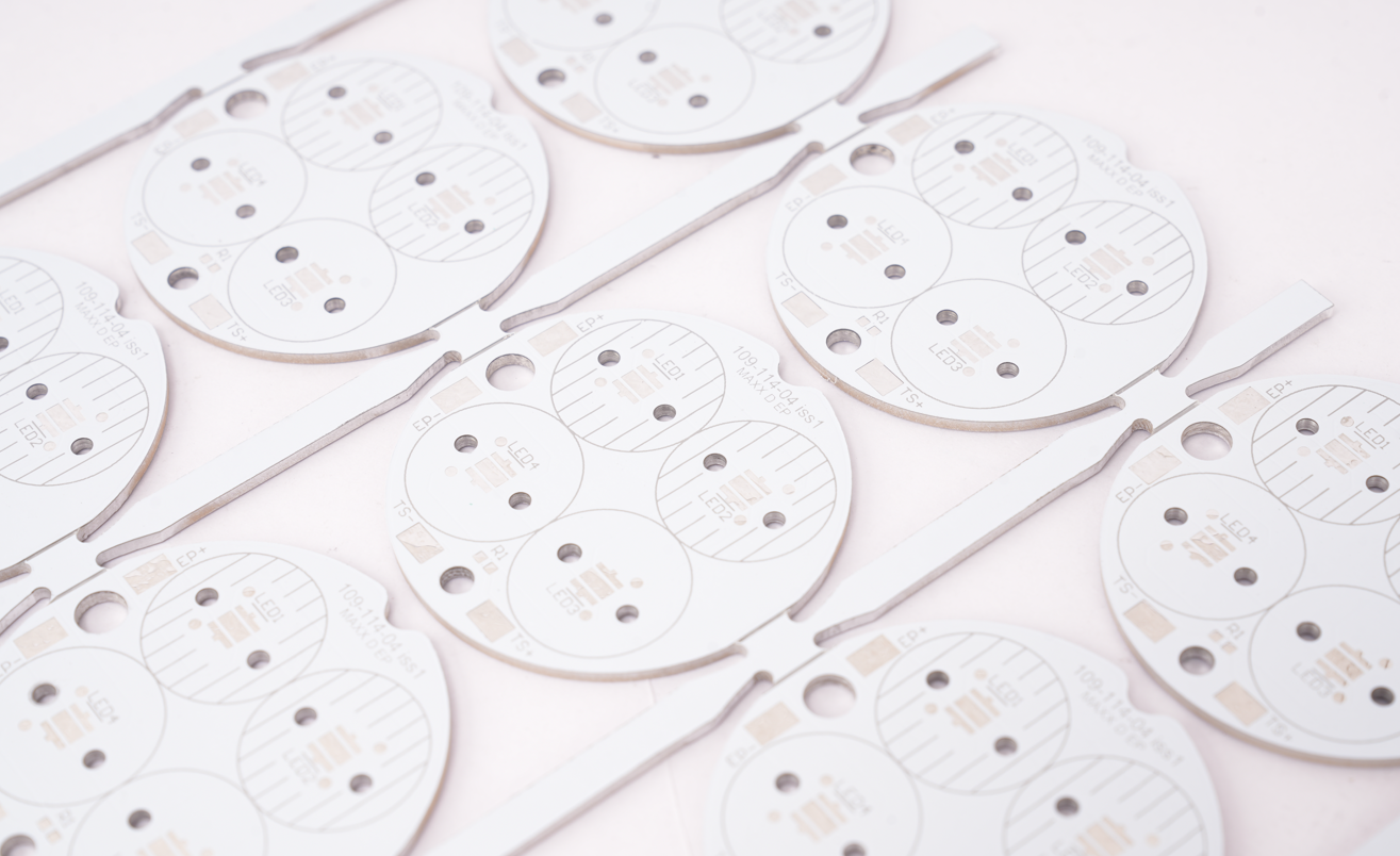
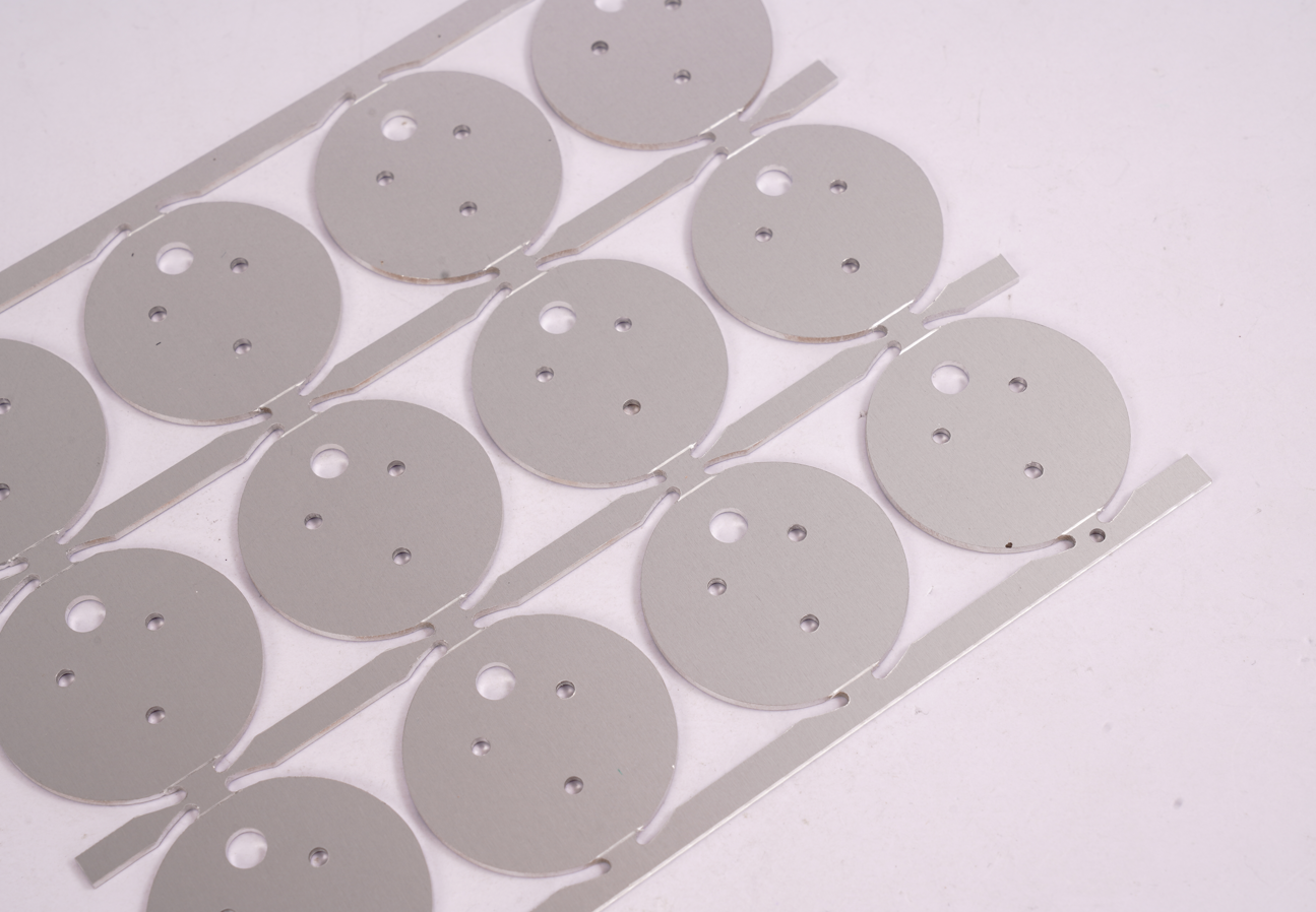
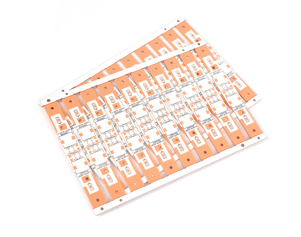
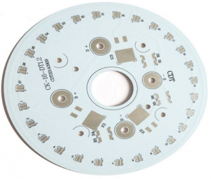
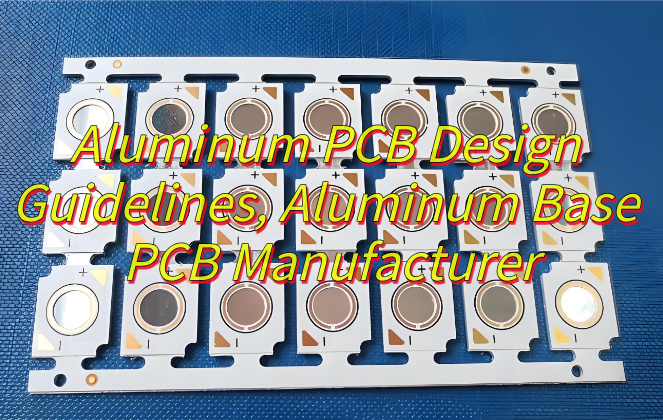
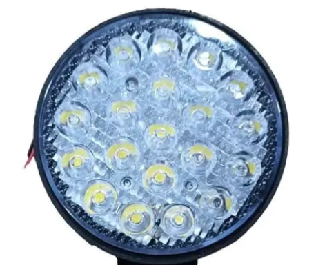
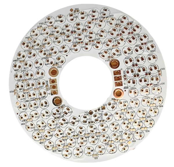
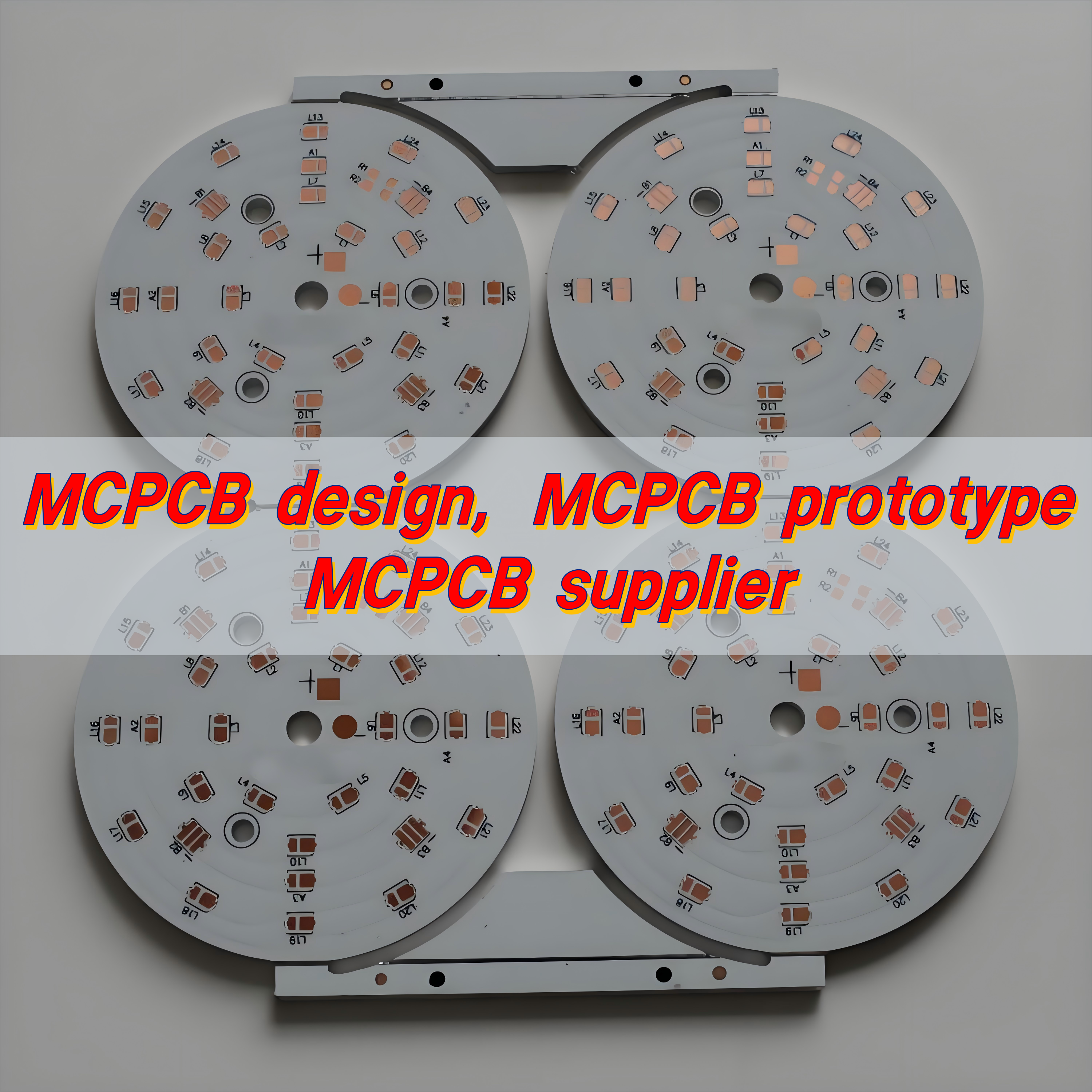
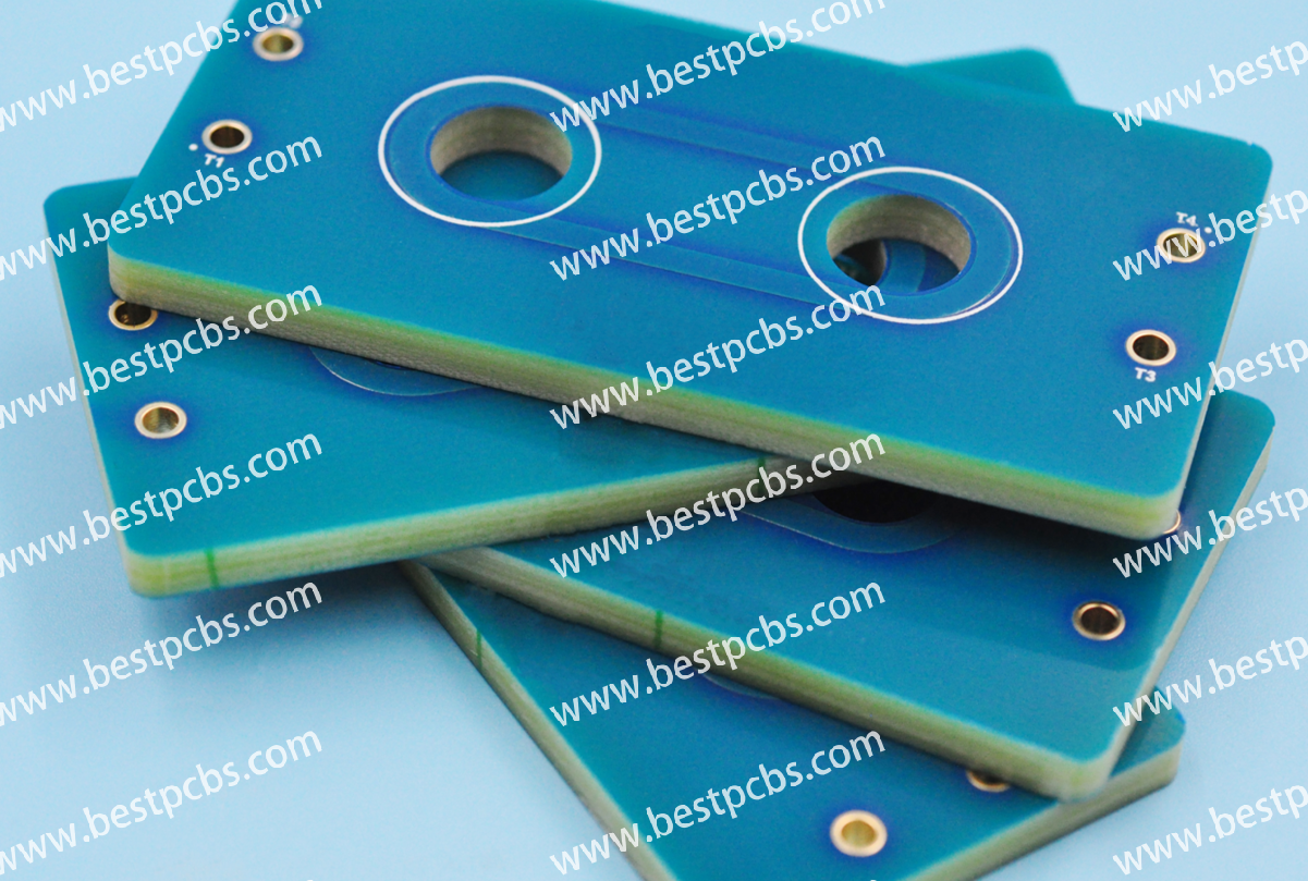
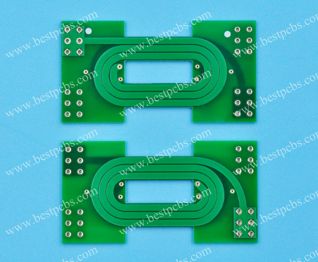
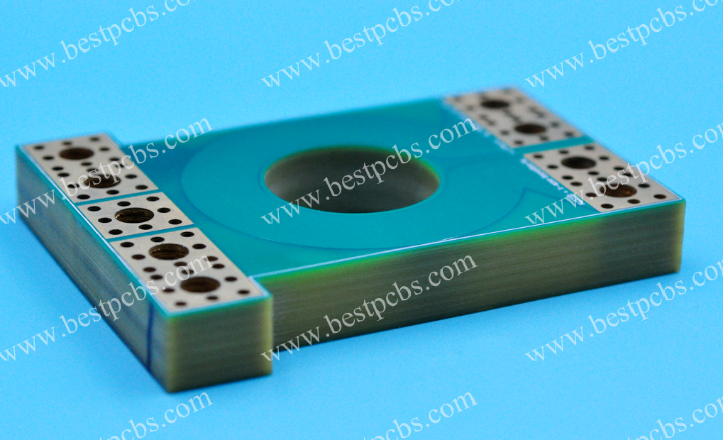
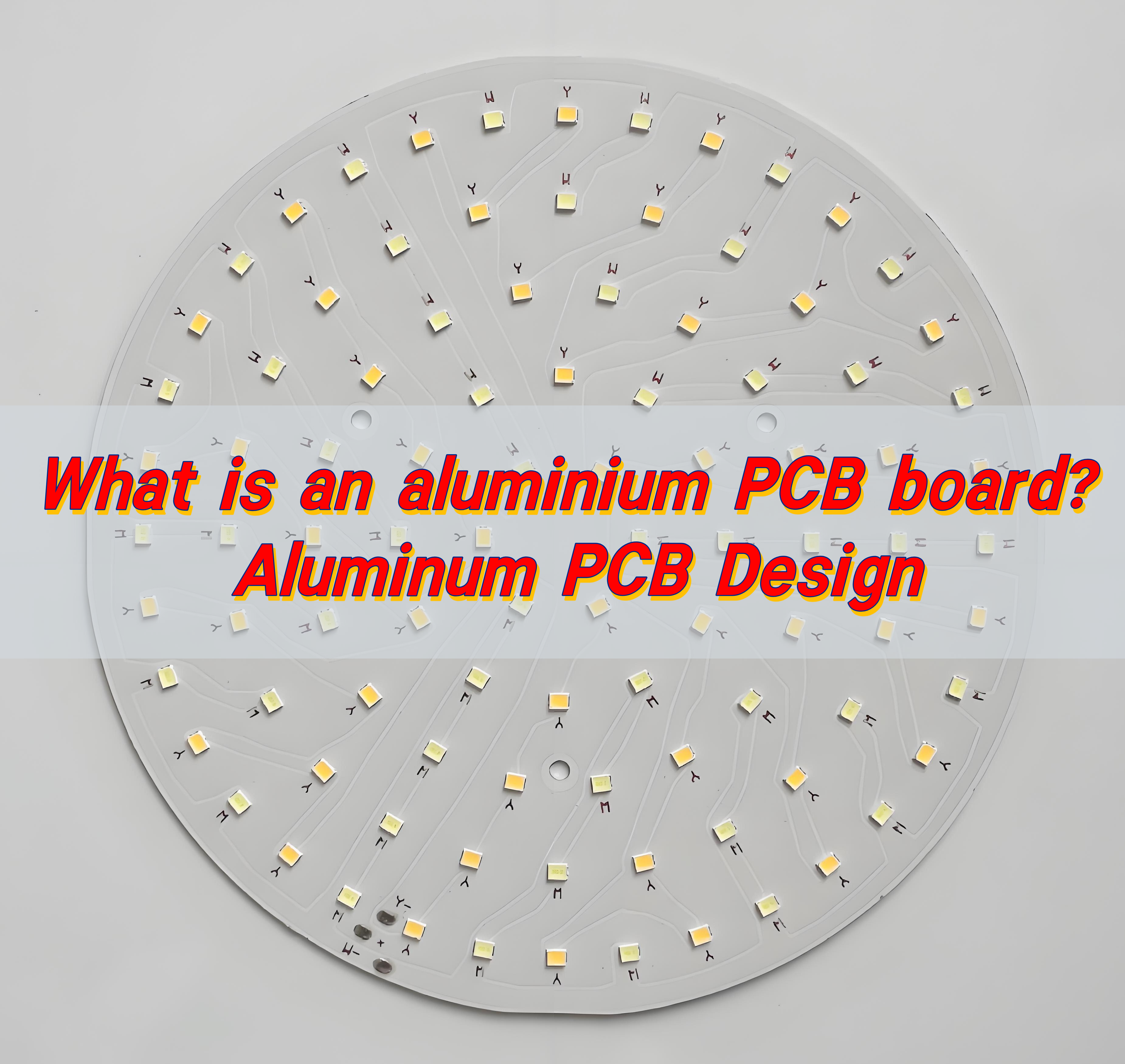
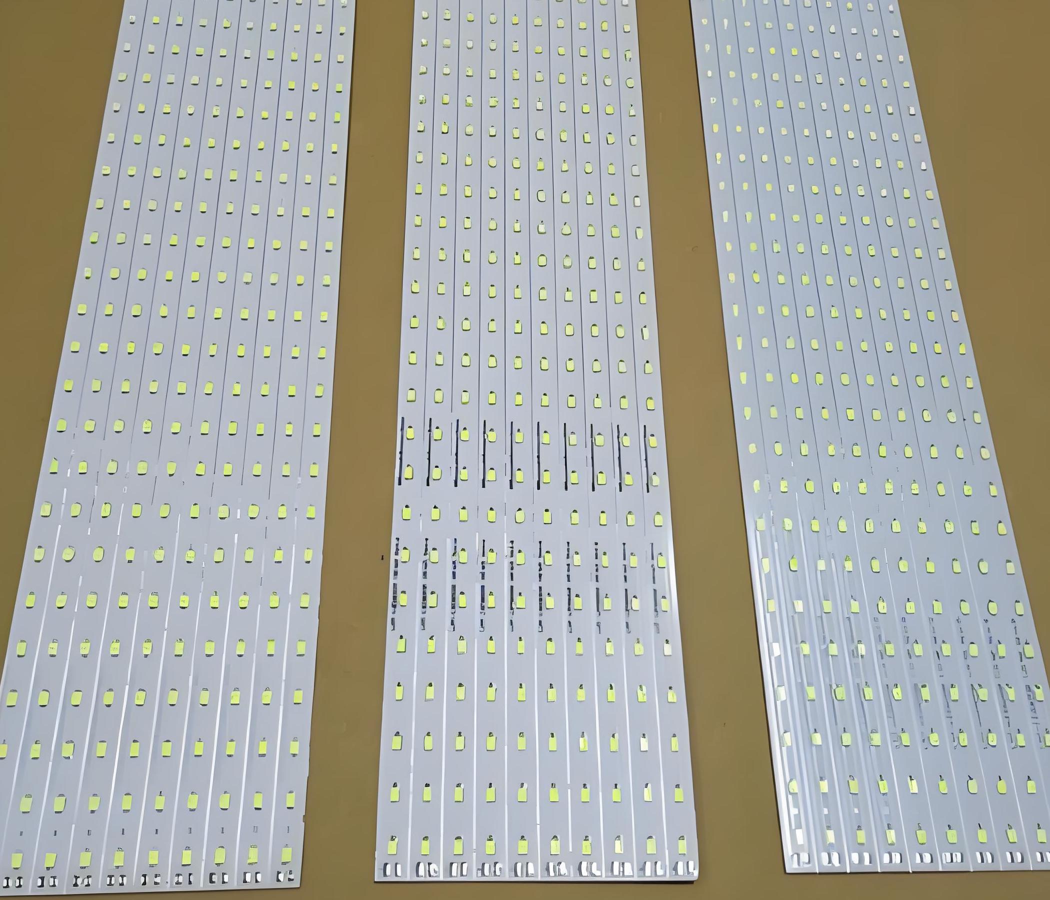
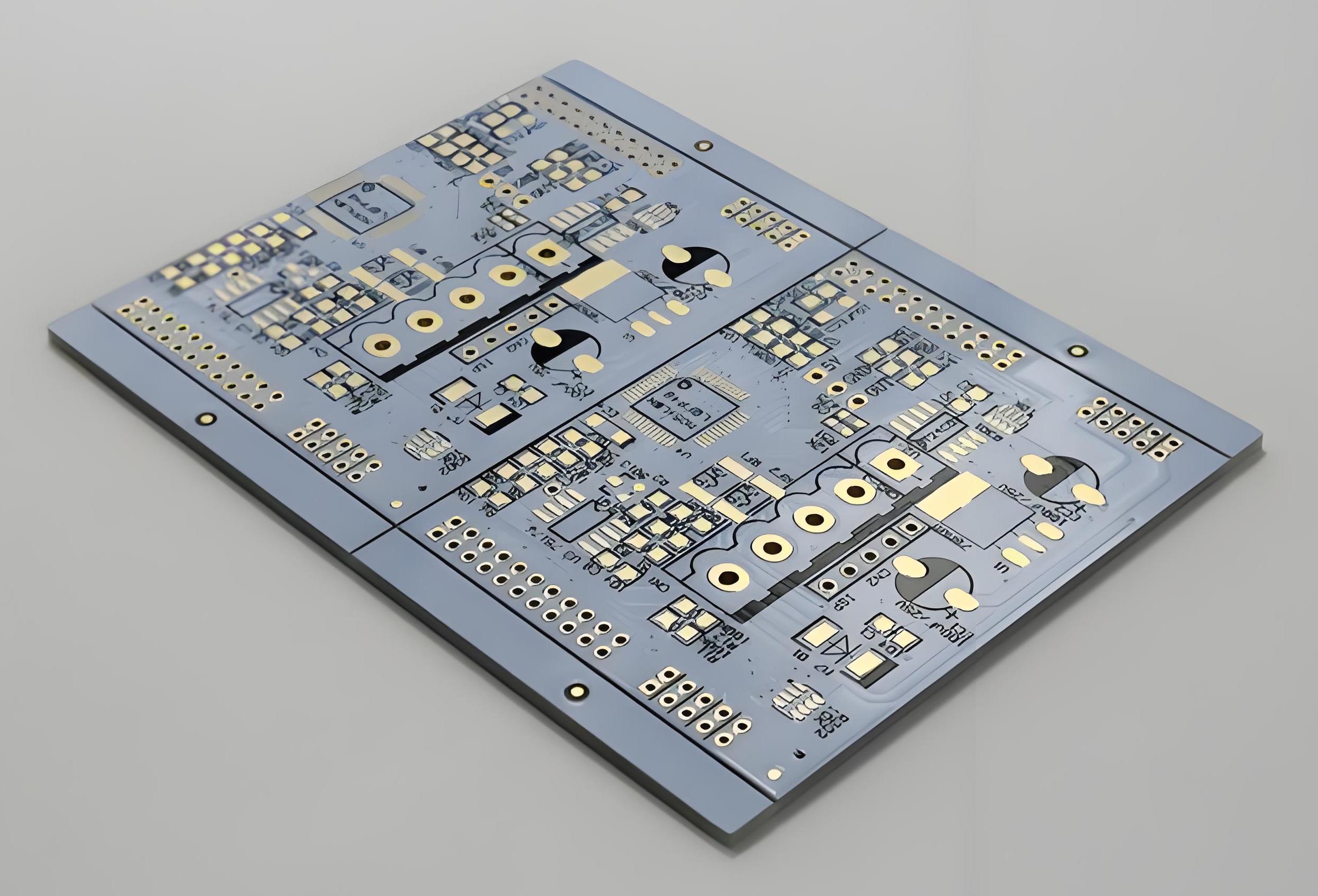
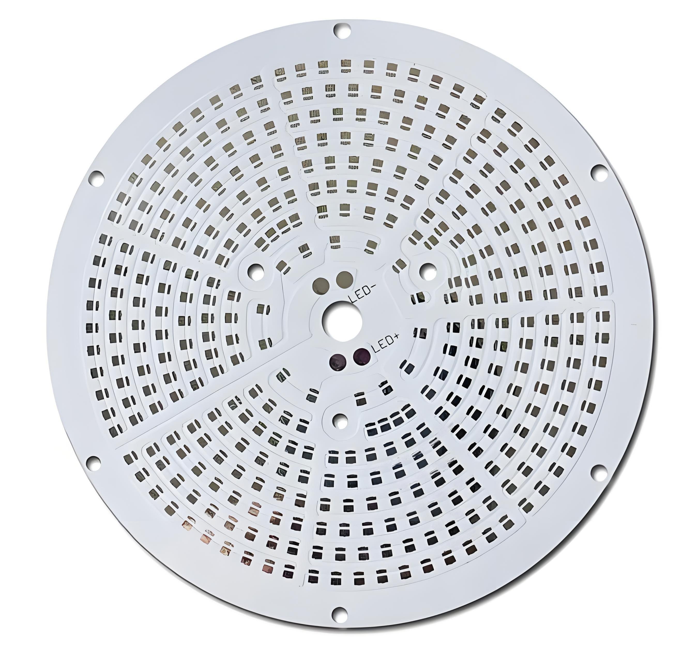
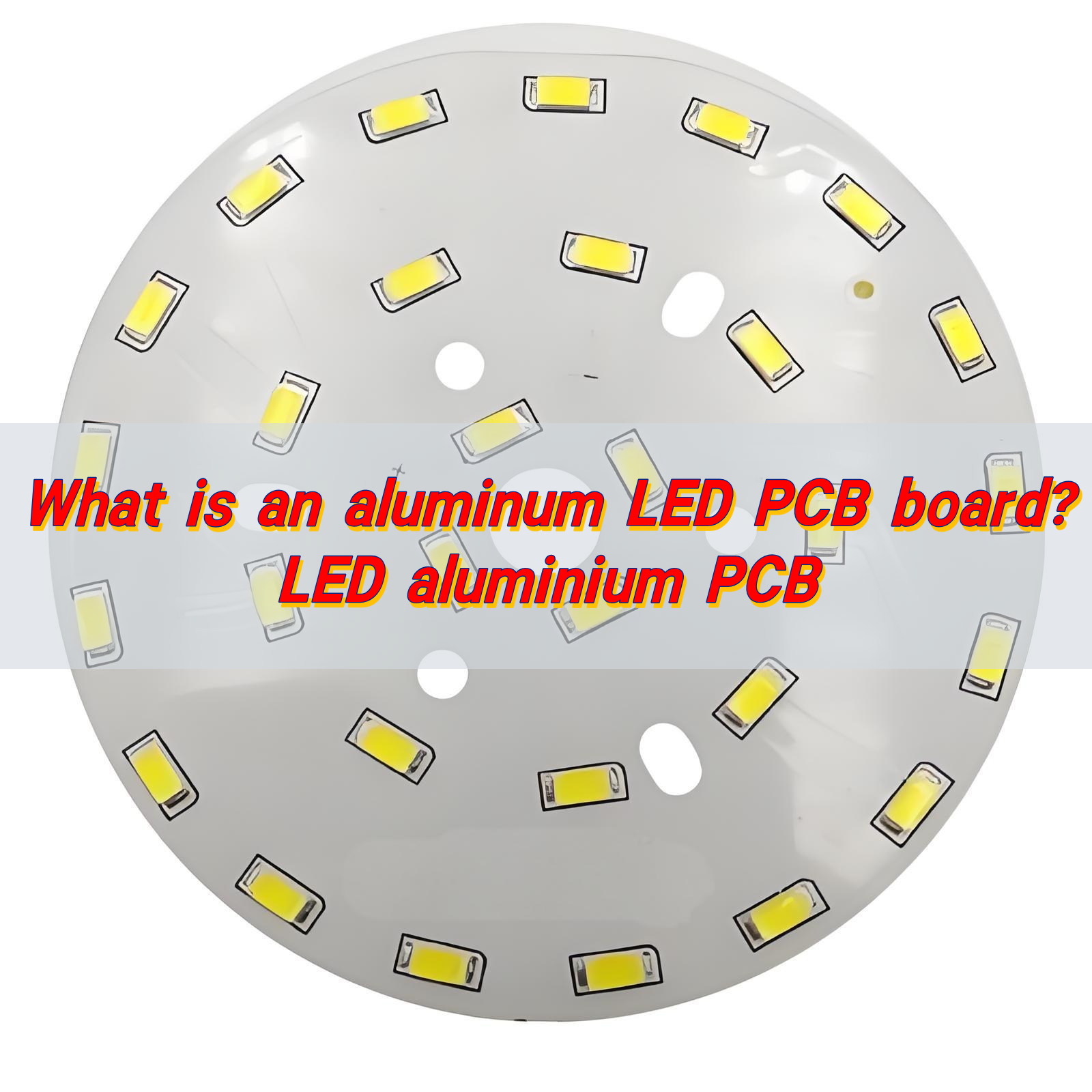
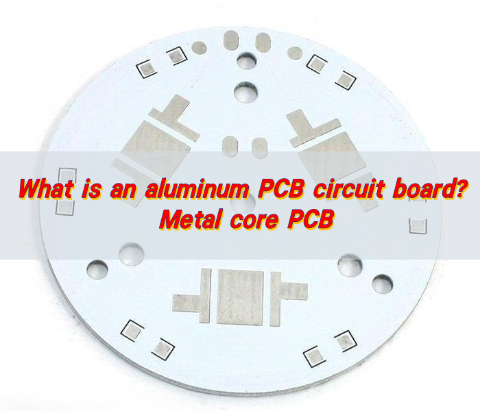
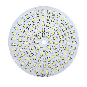
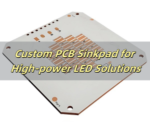
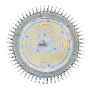
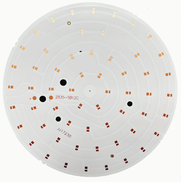
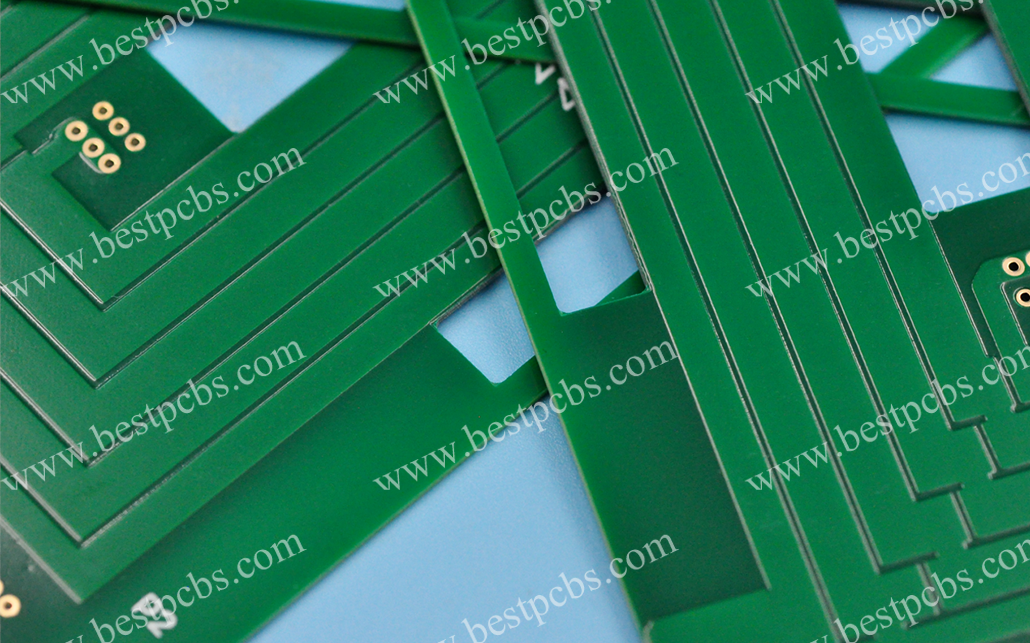
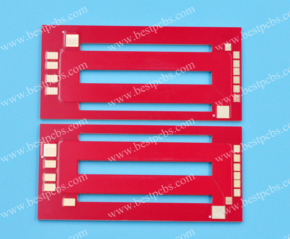
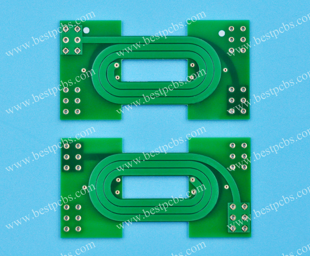
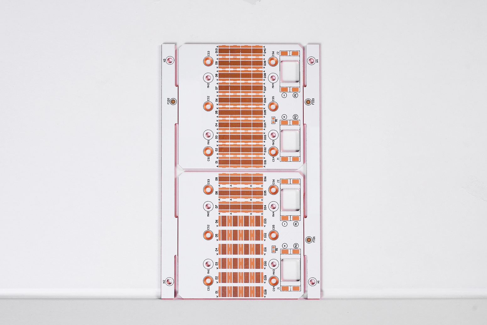
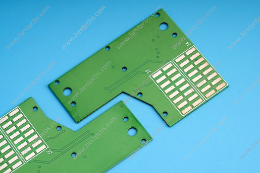
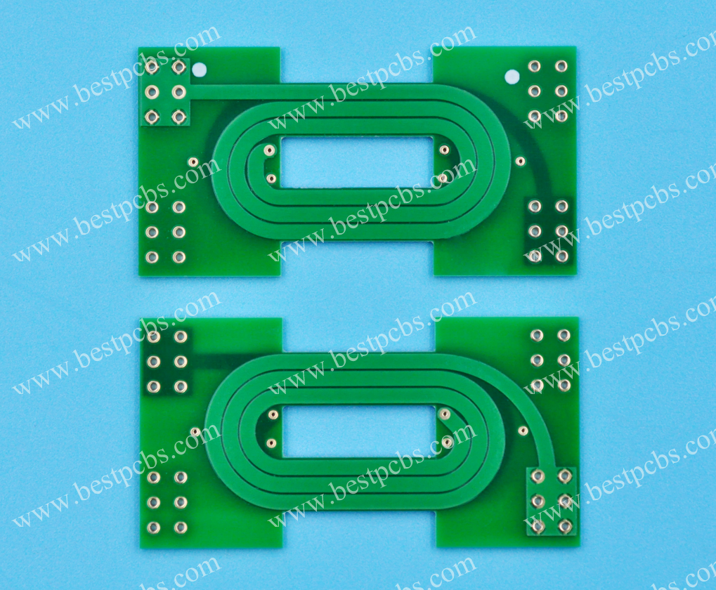
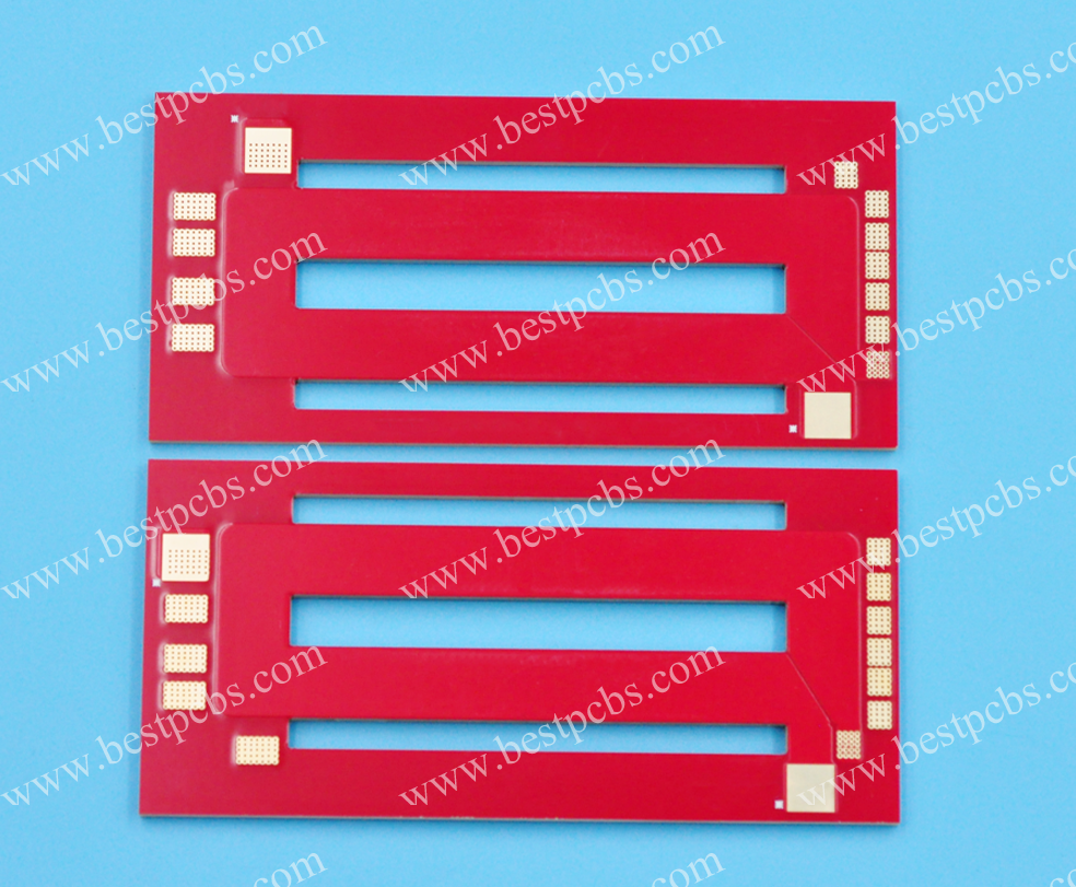
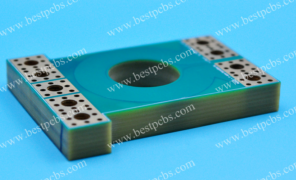
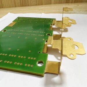
Metal Core Printed Circuit Boards (MCPCBs) are widely used in high-power applications like LED lighting, automotive systems, and power electronics. They offer superior thermal management compared to standard FR4 PCBs, but several variables impact their final pricing. Whether youâre prototyping or placing a volume order, understanding these factors helps you make informed decisions and avoid unexpected costs.
At EBest Circuit (Best Technology), we manufacture a wide range of MCPCBs tailored to customer requirements. Below, weâve broken down the main elements that influence pricing so you can better evaluate your design options.
Key Technical Factors That Affect MCPCB Pricing
1. Board Dimensions
Size is the starting point for cost evaluation. For non-rectangular shapes like circles, pricing is based on the longest two sidesâtypically the diameter for round boards. Larger boards require more base material and longer processing time, which increases the unit price.
2. Copper Thickness
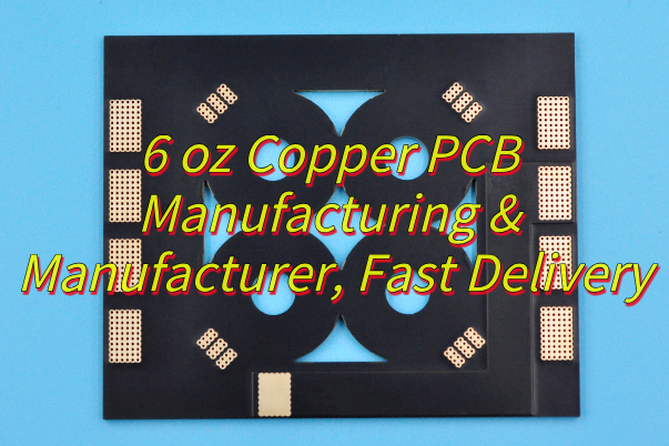
Copper thickness directly affects both thermal performance and cost. We offer standard and high-current options, including 0.5 OZ, 1 OZ, 2 OZ, 3 OZ, up to 8 OZ. Thicker copper enhances current-carrying capacity but also raises the complexity and expense of manufacturing.
3. Thermal Conductivity
A higher thermal conductivity helps to dissipate heat more efficiently. For example, 3W/m·K materials offer better heat transfer but are more expensive than standard options. The choice often depends on the power density of your application.
4. Surface Finishing
We support finishes such as HASL_LF (lead-free hot air leveling), OSP (Organic Solderability Preservative), and ENIG (Electroless Nickel Immersion Gold). ENIG is the premium choice due to its excellent solderability and oxidation resistance, though it comes at a higher cost.
5. Board Thickness
The most common MCPCB thickness is 1.6mm ±10%, which meets most design standards. Boards thinner than 1mm or thicker than 2mm will cost more due to non-standard processing. Our maximum capacity reaches 4.0mm ±10% for specific projects.
6. Solder mask Type and Color
Solder mask adds not only a protective layer but also an aesthetic touch. We offer white, black, blue, green, and red options. For high-end applications like LED boards, Taiyo solder mask is preferred for its excellent reflectivity, though it is priced higher than regular options.
7. Stack-Up and Construction
The complexity of the PCB stack-up has a big impact on both cost and manufacturing time. Single-layer boards are simpler and cheaper, while multi-layer, double-sided, or heat sink-integrated boards increase the number of processes, materials, and quality inspections required.
MCPCB Types We Offer
Our company specializes in producing a wide range of MCPCB types to suit various thermal and mechanical requirements:
Single Layer MCPCB
Two Layers MCPCB
Double-Sided MCPCB
Multi-Layer MCPCB
Chip-on-Board (COB) MCPCB
Heat Sink Integrated MCPCB
Each type is customizable to your exact application needsâwhether you’re building high-power LED lighting, automotive electronics, or power conversion devices.
How to Choose the Right Parameters Without Overspending?
When planning your MCPCB project, it’s essential to balance performance requirements with budget constraints. Here are a few suggestions:
Match copper thickness to your current needs â don’t over-specify if lower OZ will suffice.
Select surface finishing based on reliability needs â use ENIG for sensitive components, OSP for more budget-friendly builds.
Ask about solder mask options early â especially for LED projects requiring high reflectivity.
Consider standard thicknesses â unless your application has unique structural or thermal demands.
Let us help with stack-up decisions â especially for complex or multi-functional boards.
At EBest Circuit (Best Technology), we guide you through each stage of development, offering design support, material recommendations, and volume-based quotations that match your project goals.
Need help optimizing your MCPCB design for performance and cost?
Contact our team today for a fast, professional quote and expert guidance tailored to your application.
PCB contract manufacturing is a process where companies outsource the production of printed circuit boards to a third-party manufacturer. This includes not just making the board, but also assembling components, running functional tests, and sometimes even final product packaging. It allows companies to focus on core tasks like product development and marketing, while the technical side of electronics production is handled by experts.
At its core, PCB contract manufacturing saves time, reduces production costs, and ensures consistency in quality. For startups and global electronics brands alike, finding a dependable contract manufacturer can significantly boost speed-to-market and reduce project risks.
What Is PCB Contract Manufacturing
Our Printed Circuit Board Services
At EBest Circuit (Best Technology), we offer a complete range of services under one roof. Whether you’re developing a new electronic product or scaling up production, we handle everything from the initial design to final functional testing. Hereâs what we bring to the table:
PCB Layout & Design
We help you start from scratch or improve your existing Gerber files. Our layout team is experienced in high-density routing, impedance control, and EMC-compliant designs. With tools like Altium Designer and CAD, we ensure accurate and efficient PCB layouts tailored to your project needs.
OEM & ODM PCB Manufacturing
Whether you need OEM or ODM service, we have the capability to take your concept and turn it into a working product. Our engineering team collaborates closely with clients to deliver custom solutions that are production-ready.
Electronic Components Assembly
From SMT (Surface Mount Technology) to through-hole assembly, our facility is equipped for full-scale PCBA (Printed Circuit Board Assembly). We support both leaded and RoHS-compliant assembly and offer automated inspection (AOI), X-ray, and BGA rework services to guarantee every joint is solid and reliable.
Wire Harness Assembly
We also supply PVC/PE/TPU/LZSH hook-up wire, flat cable, connector wire harness for machinery equipment, and cables for the field of electronic appliances, DC power supply, audio video devices, toys, medical equipment, communication devices, electrician & electrical, computer accessories cable, and so on.
Box Building Assembly
We donât stop at the board level. If you need enclosure integration, cable harnessing, or full unit assembly, our box building assembly service is available. This end-to-end solution simplifies your supply chain and gives you more control over the finished product.
Functional Testing
We provide full functional testing based on your test procedure or help you develop one. This includes power-on tests, signal integrity verification, and custom fixture testing. We ensure your board works perfectly before it reaches your customers.
Our Printed Circuit Board Services
What PCBs We Can Fabricate?
Our team at EBest Circuit (Best Technology) specializes in a wide range of printed circuit board types. No matter your projectâs complexity or environment, weâve got you covered. Here are some products that we can make, but not limited to these PCBs.
Extra Thin PCB
For devices that require tight packaging like smart cards, cameras, or medical sensors, we offer ultra-thin PCBs as thin as 0.1mm. These boards maintain strength while saving space.
HDI PCB
High-Density Interconnect (HDI) PCBs support advanced electronics with fine-pitch components, blind and buried vias, and micro-via-in-pad technology. These are perfect for smartphones, tablets, and compact IoT devices.
RF PCB
We manufacture RF (Radio Frequency) PCBs using low-loss materials like Rogers, Taconic, and PTFE laminates. These boards are designed for wireless communication, antennas, and radar systems, where signal clarity matters most.
Heavy Copper PCB & Busbar PCB
When high current is involved, such as in automotive or industrial power supplies, heavy copper and busbar PCBs are necessary. We can produce boards with copper thickness from 2oz to 20oz, ensuring excellent thermal and electrical performance.
Metal Core PCB
For LED lighting and power conversion applications, our metal core PCBs (MCPCBs) provide efficient thermal dissipation. Aluminum and copper cores are both available depending on your thermal and mechanical needs.
Ceramic PCB
Using materials like aluminum nitride and alumina, ceramic PCBs deliver outstanding heat resistance and insulation. We have mature manufacturing technologies, including: Thick film ceramic PCB, thin film ceramic PCB, AMB ceramic PCB, DBC & DPC ceramic PCB, HTCC & LTCC ceramic PCB.
Flex Circuit & Rigid-Flex PCB
Flex circuits offer excellent bendability, reducing connectors and saving space. Rigid-flex PCBs combine the best of both worlds and are widely used in wearables, drones, and other portable electronics.
High-Speed PCB
We design and produce high-speed PCBs with controlled impedance, low-loss materials, and proper stack-ups. These are ideal for applications like 5G networks, servers, and high-frequency digital communication.
High TG PCB
When operating temperatures exceed 170°C, High-TG (glass transition temperature) PCBs are the right choice. These boards are more stable thermally and mechanically, perfect for automotive and industrial applications.
IC Substrate
We also support packaging solutions with IC substrates that act as a bridge between chips and PCBs. Our substrates offer fine-line traceability and are used in semiconductor packaging.
Ceramic Packages
Ceramic packages provide superior hermetic sealing and thermal cycling endurance. These are used to package sensitive ICs in defense, aerospace, and critical medical applications.
FR4 PCB Capability in EBest Circuit (Best Technology)
At EBest Circuit (Best Technology), we offer a wide range of FR4 PCBs â the most common material in the PCB industry â from consumer electronics to industrial control systems and automotive electronics. Whether it’s single-sided, double-sided, or multi-layer (up to 40 layers), we provide:
✅ General Capabilities
Layer Count: 1â40 layers
Board Size: Up to 580mm Ă 1200mm
Board Thickness: 0.2mm to 3.2mm
Copper Thickness: 0.5oz to 6oz (outer), 0.5oz to 3oz (inner)
Finished Hole Size: â„ 0.10mm
Minimum Line Width / Spacing: 3mil / 3mil (0.075mm)
Aspect Ratio: Up to 12:1
Impedance Control: ±10% or better
✅ Material Options
Standard FR4: Tg135°C
High-TG FR4: Tg170°C to Tg180°C
Halogen-Free FR4: Environmentally friendly for RoHS/REACH applications
Low Dk/Df FR4: For better signal performance in high-speed circuits
✅ Surface Finishes
HASL (Hot Air Solder Leveling) â Leaded & Lead-free
With a monthly capacity of over 30,000 square meters and a 98% on-time delivery rate, our FR4 line is built to serve both prototypes and mass production.
Certifications & Quality Assurance in PCB Manufacturing
At EBest Circuit (Best Technology), quality isnât just a goal â itâs a standard built into every step of our manufacturing process. To ensure compliance with international regulations and industry-specific requirements, we maintain a comprehensive set of certifications, including:
IPC Standards Compliance – IPC-A-600 and IPC-A-610 Class 2 & Class 3 for PCBfabrication and assembly
One-Stop High-Quality PCB Contract Manufacturer
When you’re looking for a reliable partner to handle your PCB contract manufacturing, EBest Circuit (Best Technology) is ready to deliver more than just boards. We provide full-service support â from design to delivery â with speed, precision, and attention to detail.
We offer a complete solution that includes PCB fabrication, components sourcing, assembly, testing, and even box build â all under one roof. That means you donât have to juggle multiple suppliers or waste time coordinating between factories. You get a dedicated project manager, clear communication, and consistent quality from start to finish.
Engineering Support: this isnât traditional engineer support, in EBest Circuit (Best Technology), every sales are engineer, they are professional so that can save much time on design communication and can give you the best solutions.
Fast Turnaround: we offer quick-turn prototyping (as fast as 24 hours) and competitive lead times for volume production.
Global Shipping: Whether youâre in the US, Germany, Japan, or Australia, we ship your orders promptly with DHL, FedEx, UPS, air & ocean shipment.
Traceability System: Our ERP system keeps detailed records for every board we produce, offering transparency and traceability.
WIP Update Every Week: Every customer can enjoy one-to-one sales-assistant service, they will update the product status & share videos every week for you, so that you can closely to your PCBs.
Cost-Effective Solutions: With advanced production lines and a mature supply chain, we provide cost-effective options without sacrificing quality.
PCB contract manufacturing can significantly reduce your product development cycle and overhead. By partnering with a professional and certified provider like EBest Circuit (Best Technology), you ensure every step â from PCB layout to functional testing â meets your project goals with precision and speed.
Whether you need a simple FR4 board or a high-performance ceramic PCB, our comprehensive services and commitment to quality make us a trusted choice for businesses around the world.
Frequently Asked Questions
1. What industries does EBest Circuit (Best Technology) serve?
We serve a broad range of industries including medical, automotive, aerospace, telecom, and consumer electronics.
2. Can EBest Circuit (Best Technology) support low-volume or prototype orders?
Yes, we support both small-batch prototypes and high-volume production with flexible minimum order quantities.
3. Do you offer component sourcing services?
Absolutely. We have partnerships with authorized distributors to source genuine components and manage the BOM for you.
4. What file formats do you accept for PCB layout?
We accept Gerber, ODB++, and other formats such as Altium, Eagle, and CAD-based files.
5. How can I request a quote for PCB contract manufacturing?
Simply send your files and requirements via our online form or email, and our sales team will get back to you within 24 hours.
Why is embedded PCB designthe future of compact electronics?â This guide covers aspects from design tools to thermal optimization and non-destructive testing.
EBest Circuit (Best Technology) sets the industry benchmark for rapid embedded PCB manufacturing by consistently delivering complex designs 40% faster than competitors without compromising IPC Class 3 standards. Our proprietary “Speed-Stack” manufacturing system integrates AI-driven design validation, in-house laser micromachining, and pre-tested component libraries to slash typical 6-week lead times to just 10 business days. With 24/7 manned production lines and drone-assisted logistics, we’ve achieved a 99.8% on-time delivery rate for over 2,300 embedded PCB projects in 2024, including mission-critical medical and aerospace applications. Clients benefit from our real-time production tracking portal and guaranteed 72-hour prototype turnaround– a capability validated by three patents in accelerated multilayer bonding and high-speed impedance testing. Welcome to contact us: sales@bestpcbs.com.
What Is Meant by Embedded PCB Design?
Embedded PCB design refers to the process of integrating electronic components directly into the layers of a printed circuit board (PCB). This approach allows for a more compact, efficient, and reliable electronic system. Instead of having components mounted on the surface or through holes of the PCB, they are embedded within the board’s structure. With embedded PCB design, you can achieve better electrical performance, reduce electromagnetic interference, and enhance the overall durability of the PCB. This type of design is becoming increasingly popular in various industries, from consumer electronics to aerospace, as it enables the creation of smaller, faster, and more power-efficient devices. Embedded PCB design is not just about placing components; it involves careful planning and engineering to ensure that all elements work harmoniously together within the confined space of the PCB.
How to Choose Embedded PCB Design Tools?
Functionality: Choose tools that support component embedding, high-speed signal processing of multilayer boards, and impedance matching calculations. For example, Altium Designer’s Component Placement Editor can achieve precise embedding, and PADS Professional’s interactive routing can handle complex topologies. At the same time, ensure that the tool has SPICE-level circuit simulation capabilities to verify power integrity and signal quality in advance.
User Interface: Give priority to tools that can customize shortcut keys and workspace layouts, such as KiCad, which supports users to save personalized interface configurations. It is recommended to use a router with real-time preview function, such as Eagle’s automatic push routing, which can intuitively see the routing effect and reduce rework.
Compatibility: Confirm that the tool supports mainstream format conversion, such as Gerber RS-274X output and STEP 3D model import. Design tools integrated with common version control tools (such as Git) can achieve file version traceability during team collaboration. Avoid using tools that only support proprietary formats to prevent data migration difficulties.
Scalability: When dealing with high-density designs with more than 5,000 components and more than 20 layers, the tool should be able to run smoothly on an ordinary workstation (more than 16GB of memory). It is recommended to choose tools that support distributed computing, such as Cadence Allegro, which can use multi-core CPUs to accelerate DRC checks and avoid lags in large projects.
Support and Updates: Choose vendors that provide quarterly security patches and feature updates, such as Mentor Graphics, which releases 2-3 major version updates per year. Make sure the vendor provides a 24-hour technical support channel that can quickly respond to DRC errors, library file compatibility and other issues through online work orders, phone calls, etc.
Cost-effectiveness: Startup teams can consider open source tools (such as KiCad) or subscription services (such as Altium Designer, which is paid monthly) to avoid high one-time investments. When comparing tools, focus on calculating the usage rate of functions. For example, if only basic routing functions are used each month, expensive full-featured kits will be wasted.
Community and Resources: Choose tools with active code maintenance on GitHub and dedicated sections on Stack Exchange. For example, the Easy EDA community updates 10+ practical cases every day, and its official knowledge base contains complete tutorials from entry to high-speed design, making it easy for designers to quickly solve common problems.
What Is the Design Process for Embedded PCB?
Below are design processes for Embedded PCB:
Requirements gathering: The first task is to clarify the requirements of the embedded printed circuit board (PCB). This requires not only a deep understanding of the electrical parameters of the final product, such as operating voltage, current, signal frequency, etc., but also mechanical constraints, such as PCB size, shape, mounting hole location, etc., as well as clear performance expectations, such as processing speed and stability requirements. Accurately grasping the functional goals of the PCB is the cornerstone of ensuring the success of embedded PCB design.
Component selection: When selecting suitable electronic components for embedded design, many factors need to be considered comprehensively. The physical size of the component must fit the compact PCB space layout; the power consumption index must meet the device endurance and heat dissipation requirements; the functional characteristics must accurately match the design requirements. In addition, the selected components should also be compatible with the embedding process to ensure that they can meet the overall design standards of the embedded PCB.
Schematic design: Draw a detailed circuit schematic to clearly present the electrical connection relationship between all components. This link is a key step to ensure the normal operation of the embedded PCB function. A well-designed schematic, like a construction blueprint for subsequent layout design, lays a solid foundation for the entire design process.
Layout planning: When planning the layout of an embedded PCB, you need to consider all factors such as component placement, wiring channels, and power distribution. Reasonable optimization of the layout can effectively reduce mutual interference between signals on the one hand, and ensure efficient heat dissipation on the other hand. Excellent layout planning is the core of achieving high-performance embedded PCBs.
Component embedding: According to the design plan, the selected components are accurately integrated into each layer of the PCB. This process relies on high-precision manufacturing processes to ensure that the components are firmly embedded and reliable electrical connections are achieved. The quality of component embedding will directly affect the operational reliability of the embedded PCB.
Routing: The electrical circuits are laid out on the PCB to connect various components. Advanced routing algorithms and technologies are used to optimize the circuits to ensure signal integrity and power transmission efficiency. As a key link in embedded PCB design, routing has a significant impact on the overall performance of the PCB.
Design rule checking (DRC): Perform design rule checking to verify whether the design strictly follows all design specifications and manufacturing requirements. Through DRC, potential problems can be discovered and corrected in time before the PCB goes into production, which is an indispensable quality control method in embedded PCB design.
Electrical simulation: Conduct electrical performance simulation analysis to explore the operating performance of embedded PCB under different working conditions. With the help of simulation, the actual working state of the PCB can be predicted in advance, and the optimization points can be accurately located, providing a strong basis for design improvement.
Mechanical design considerations: Incorporate mechanical design elements into the overall plan, including determining the thickness of the circuit board, planning the location of the mounting holes, and selecting suitable connectors. Ensure that the mechanical design is perfectly matched with the overall system requirements to ensure the installation and use of the PCB in actual applications.
Design review: Conduct a comprehensive design review with other engineers or project stakeholders. Through multi-party communication and review, problems that may be overlooked in the design can be discovered, and potential optimization suggestions can be put forward to further improve the embedded PCB design.
How to Optimize the Heat Dissipation Design of Embedded PCB?
Component Placement:
Prioritize the placement of chips with high heat generation (such as CPU, power amplifier) ââat the edge or corner of the PCB, away from temperature-sensitive components (such as crystal oscillators, sensors), with a spacing of at least 5mm.
For vertically mounted PCBs, the heat generating components should be placed at the top to dissipate heat naturally by utilizing the principle of rising hot air; when installed horizontally, the layout should be combined with the direction of the chassis air duct to ensure that the arrangement direction of the components is consistent with the direction of the airflow.
Thermal vias:
Use vias with a diameter of 0.3-0.5mm, and place 8-16 vias in an array form (recommended spacing â€1mm) under the power device to ensure that the heat conduction path between each layer of PCB is unobstructed.
For the inner power/ground layer of the multi-layer board, the inter-layer thermal coupling efficiency is enhanced by quincunx-shaped or grid-shaped via layout.
Thermal Interface Materials:
For BGA packaged chips, it is recommended to use silicone grease with a thermal conductivity of â„3W/mK, and the coating thickness is controlled at 0.1-0.2mm to ensure that the bottom of the chip is completely covered.
Install a thermal conductive silicone pad between the radiator and the PCB. Select a material with a Shore hardness of 40-60 according to the pressure requirements to effectively fill the tiny gap.
Copper Plane Design:
Lay a complete solid copper foil in the power module and processor area. The copper foil thickness is recommended to be 2oz (70ÎŒm) or more. The heat dissipation capacity is improved by increasing the copper cladding area.
For high-frequency signal areas, a grid-shaped copper cladding design is adopted, and the grid width is â„0.3mm to avoid affecting the signal integrity.
Ventilation Holes:
Open circular ventilation holes with a diameter of 1-3mm in the concentrated heat generation area of ââthe PCB, and the hole spacing is maintained at 5-10mm to form a honeycomb array structure.
The ventilation hole layout needs to avoid the signal line, power line and pad area, and the mechanical strength is enhanced by adding a teardrop structure.
Component Selection:
Give priority to low-power devices, such as using TDFN packages instead of traditional DIP packages, which can reduce thermal resistance by more than 30%; select QFN package ICs with heat dissipation pads, which are directly thermally connected to the PCB.
Perform thermal performance tests on key components to ensure that their junction temperature is lower than the maximum allowable value specified in the data sheet when running at full load (usually derating by 20%).
Thermal Simulation:
Use professional simulation software such as ANSYS Icepak, input actual working environment parameters (ambient temperature, wind speed, altitude, etc.), and establish a 3D thermal model.
For high-temperature areas (over 85°C) displayed in the simulation, iterative optimization is performed by adding heat dissipation vias, adjusting the copper foil area, or optimizing the air duct design until the thermal design goals are met.
Experience and Expertise: Choose a manufacturer with a solid track record in embedded PCB design. Years of experience translate to the skills needed for complex projects, ensuring designs that meet your requirements.
Technology and Equipment: Prioritize manufacturers with state – of – the – art facilities and the latest design software. Advanced tech enables precise, efficient manufacturing.
Quality Control: Choose a manufacturer with strict quality control at every stage. This guarantees high – quality, defect – free embedded PCBs.
Customization: Ensure the manufacturer can tailor designs to your unique needs. Customization increases the chances of getting a product that matches your expectations.
Turnaround Time: Consider manufacturers that offer timely delivery, especially for projects with tight deadlines. Fast, quality service is key.
Cost – effectiveness: Look for competitive pricing, but don’t sacrifice quality. Compare costs while evaluating services offered.
Customer Support: Select a manufacturer with responsive customer service. They should assist throughout the process and resolve issues promptly.
Certifications and Portfolio: Check for relevant certifications like ISO 9001 and IPC standards. Review their project portfolio to assess capabilities and past work quality.
How to Test Embedded PCB Without Destructive Rework?
In-circuit testing (ICT): Use an in-circuit tester to detect the circuit connection and component function of the embedded PCB. This non-destructive testing method can quickly locate problems such as short circuits, open circuits, component parameter errors, etc. For example, when batch testing on the production line, unqualified boards can be found in the first place.
Flying probe test: Use movable probes to detect PCBs point by point, which is suitable for complex or embedded PCBs in the proofing stage. For small batches of customized boards, there is no need to make expensive test fixtures, and comprehensive testing can be completed by flexibly moving the probes.
Functional test: Input a specific signal to the PCB to observe whether the output meets the design requirements. For example, when testing a communication module PCB, after sending a data instruction, check whether the response is returned correctly to ensure that each functional module is working properly.
Boundary scan test (JTAG): Mainly checks the connection between components on the PCB. Sending test signals through the JTAG interface can detect problems such as pin solder joints and line breaks even if the component pins are covered by the package.
Thermal imaging detection: Use a thermal imager to scan the temperature distribution on the PCB surface. Once an abnormal hot spot is found, it may be due to component overload or heat dissipation design defects. For example, if the temperature near the processor is too high, it is necessary to check the heat sink installation or thermal design problems.
Visual inspection: Manually check the appearance of the PCB carefully to check for obvious defects such as line breakage, component warping, and solder joints. This is the most basic detection step and can quickly find assembly problems in the production process.
Impedance test: Measure the impedance value of PCB lines and components. If the impedance does not meet the standard, it may affect signal transmission. For example, the impedance of the differential line of a high-speed PCB is abnormal, which will cause data transmission errors.
Signal integrity test: Analyze the attenuation, reflection, and crosstalk of the signal during PCB transmission. For high-frequency circuits, capture the signal waveform through an oscilloscope and other devices, and optimize the wiring design to ensure signal quality.
Power-on self-test (POST): Automatically run the self-test program when the embedded system starts. The moment the system is turned on, you can quickly check whether the basic functions of the PCB are normal, such as detecting modules such as memory and CPU.
Aging test: Put the PCB in a high-temperature environment and run it continuously for several hours or even days. Simulate long-term use scenarios to expose early potential failures in advance. For example, the aging test of newly produced industrial control boards can greatly improve the stability of later use.
Can Your Manufacturer Provide PCB Design Embedded Hardware Services?
Yes, EBest Circuit (Best Technology) also can indeed provide all these services:
Design Consultation: Our team of experienced engineers at EBest Circuit (Best Technology) has extensive know – how in embedded PCB design. We offer in – depth design consultation, analyzing your initial concepts from multiple perspectives such as signal integrity, power management, and thermal performance. This helps you refine your design to be more efficient and reliable right from the start.
Component Sourcing: Leveraging our well – established global supplier network, we assist you in sourcing high – quality components at competitive prices. We ensure that the components used in your embedded PCB design are of the best quality, meeting industry standards and contributing to the optimal performance of your product.
Prototyping: With prototyping facilities, EBest Circuit (Best Technology) offers rapid prototyping services. This enables you to test the functionality and performance of your embedded PCB design promptly. Our state-of-the-art equipment and skilled technicians guarantee accurate prototypes with short turnaround times, allowing you to quickly move on to the next stage of development.
Design for Manufacturability (DFM) Analysis: Our reliable team conducts thorough DFM analysis on your embedded PCB design. By carefully examining the design for potential manufacturing bottlenecks, we identify and address issues early on. This proactive approach ensures a seamless manufacturing process, reducing costs and minimizing delays.
Assembly and Testing: EBest Circuit (Best Technology) provides comprehensive assembly and testing services for embedded PCBs. Our assembly process is carried out with precision, and we perform a wide range of tests, including functional, electrical, and environmental tests. This guarantees that the final product meets or exceeds your requirements.
Firmware and Software Support: For embedded PCB designs that require custom firmware or software, our experts are on hand to offer support. We can develop, debug, and optimize the necessary firmware and software to ensure that your design functions flawlessly.
Documentation: We understand the importance of comprehensive documentation. EBest Circuit (Best Technology) provides detailed schematics, layout files, bill of materials, and test reports for your embedded PCB design. These documents are crucial for future maintenance, upgrades, and regulatory compliance.
Scalability: Whether you need a small batch of prototypes or large scale production, EBest Circuit (Best Technology) has the capacity and flexibility to meet your needs. Our scalable manufacturing processes and resources can adapt to your changing requirements, ensuring a smooth transition from prototype to mass production.
Technical Support: Our technical support team is available throughout the design and manufacturing process. From answering your queries to resolving complex technical issues, we provide guidance and support to help you improve the performance of your embedded PCB design.
Continuous Improvement: EBest Circuit (Best Technology) is dedicated to continuous improvement. We stay updated with the latest advancements in embedded PCB design and embedded hardware services. By incorporating new technologies and trends, we enhance the quality and performance of your products, giving you a competitive edge in the market.
What Are the Main Challenges in Embedded PCB Design?
Here are the main challenges in embedded PCB design, derived from recent research and industry trends:
Signal Integrity in High-Speed Applications
Emerging standards like PCIe 5.0, USB4, and 100G+ Ethernet demand rigorous control over impedance, crosstalk, and jitter. Studies highlight that reflections caused by via stubs and connector discontinuities remain critical obstacles even with advanced materials like Megtron 7.
Thermal Management for Power Density
Compact designs incorporating GaN/SiC power devices create localized hotspots exceeding 150°C. Liquid cooling integration and embedded thermal vias are active research areas, though challenges persist in balancing performance with long-term reliability.
Miniaturization Without Compromise
HDI (High-Density Interconnect) technologies below 50ÎŒm line/space introduce yield risks. Research focuses on additive manufacturing processes but faces scalability issues for mass production.
EMI/EMC Compliance in Dense Systems
Coexistence of wireless modules (5G, Wi-Fi 6E) with high-speed digital circuits creates complex interference patterns. Machine learning-based shielding optimization shows promise but requires extensive training datasets.
Supply Chain Volatility
Component obsolescence and lead time fluctuations force designers to adopt multi-sourcing strategies. This complicates library management and increases design iteration cycles.
Design-for-Test (DFT) Complexity
System-in-Package (SiP) and 3D IC integration make traditional boundary scan insufficient. Research explores embedded test access mechanisms (eTAM) but adds significant routing overhead.
Power Integrity Across Domains
Mixed-signal designs struggle with simultaneous switching noise (SSN) affecting ADC/DAC performance. Isolation techniques using integrated transformers remain an area of active development.
Regulatory Compliance Updates
Frequent revisions to standards like IEC 62368-1 (safety) and RoHS/REACH require continuous design adjustments, particularly for automotive (ISO 26262) and medical (IEC 60601) applications.
Mechanical-Electrical Co-Design
Flexible and rigid-flex PCBs demand iterative collaboration between electrical and mechanical engineers. Simulation tools often lack real-time feedback loops between thermal stress and electrical performance.
Cybersecurity Integration
Embedded firmware security (e.g., side-channel attack prevention) now influences PCB layout. Research investigates hardware-isolated security enclaves but increases BOM costs.
Conclusion
In short, embedded PCB design is challenging, but the payoff is big. You get smaller, faster, and more reliable electronics. To make your project work, you need to know what embedded PCBs are, how to design them, and pick the right tools. Handling heat well and thorough testing are also musts. When choosing a manufacturer, look for ones with real experience, strict quality checks, and good service. Ready to start your embedded PCB project? Get in touch with EBest Circuit (Best Technology) for a quote. Our team is here to help with every step. Email us at sales@bestpcbs.com to get started.
Printed circuit board assembly PCBAÂ is a vital step between your design and a working electronic product. At EBest Circuit (Best Technology), we understand how much timing and quality matter. Our short delivery services, expert support, and cost-effective solutions have helped many clients get their innovations to market faster.
EBest Circuit (Best Technology) is an original factory offering printed circuit board assembly PCBA for the global market. We perceive that quality is our lifeline and the anchor that we gaining the trust of customers. Our facility is certified by ISO 9001, ISO 13485, IATF 16949, and AS9100D. You feel assured that we provide high-quality PCBA with short delivery. For any projects, kindly contact us at sales@bestpcbs.com at all times.
What is a Printed Circuit Board Assembly PCBA?
A printed circuit board assembly, or PCBA, refers to a finished circuit board after all the electronic components are mounted. This includes resistors, ICs, capacitors, and connectors. The PCBA stage transforms a bare PCB into a functional board ready to be used in devices.
What is the Difference Between PCB and Printed Circuit Board Assembly PCBA?
PCB is the blank board made of layers of insulating material and copper traces. It serves as the backbone of electronics. A PCBA, on the other hand, is that same board but fully populated with components. Simply put, PCBA = PCB + Assembly Process.
How Does a Printed Circuit Board Assembly PCBA Work?
The process begins with placing solder paste on pads, then mounting components using SMT or manual insertion. After that, boards are passed through a reflow or wave soldering process. Testing and cleaning ensure quality before packaging. At EBest Circuit (Best Technology), this process is handled quickly, even within 24â72 hours.
We make each step efficient with top equipment and skilled operators, helping reduce delays and rework.
What is Printed Circuit Board Assembly HS Code?
The HS code for printed circuit board assemblies is typically 8538900000. This classification helps with customs documentation and international shipping. Our team supports you with clear labeling and smooth logistics across borders.
How to Choose the Right Printed Circuit Board Assembly PCBA Partner for Your Product?
Choosing the right partner affects both product success and delivery time. Hereâs what to consider:
Turnaround speed:Â Can they deliver in 24â72 hours?
Engineering support:Â Do they help with design and DFM analysis?
Cost control:Â Do they provide cost-saving options?
Testing capability:Â Can they handle RF and EMC testing?
Experience:Â Have they managed complex builds?
EBest Circuit (Best Technology) checks all the above boxes. We donât just build boards â we help optimize them too.
Why Should You Choose EBest Circuit (Best Technology) as One of Your Printed Circuit Board Assembly Companies?
Customers working with EBest Circuit (Best Technology) often face pressure with delivery, design complexity, or rising costs. Here’s how we solve those issues:
1. Fast Turnaround in 24â72 Hours
We understand your time matters. Thatâs why we offer rapid PCBA services that can be completed within one to three days. This helps speed up prototyping, testing, and full-scale launches.
2. Full Technical Support
From layout reviews to material selection, our engineers are here to help. We work closely with your team to spot problems early and recommend smart improvements.
3. Smart Cost Control
We combine advanced manufacturing with strong supply chain management. That way, you save money without sacrificing quality.
4. RF and High-Frequency PCB Expertise
Many clients trust us for high-speed, high-frequency builds. We resolve signal loss, EMI, and impedance issues using techniques like:
45-degree routing
Proper grounding and shielding
Differential pair control
Optimized PCB stackup
5. Simulation and Testing Support
Donât wait until the final product fails. We offer signal integrity simulation and full EMC testing with equipment like TDR, VNA, and spectrum analyzers. This reduces rework and speeds up certification.
6. Advanced Manufacturing Capabilities
Our facility handles complex needs like:
Impedance-controlled multilayers
Blind/buried vias
Ultra-fine trace and spacing (±5Όm precision)
Microvia laser drilling
All are supported by ISO 9001, ISO 13485, IATF 16949, and AS9100D certifications.
7. One-Stop Service
Whether you need bare boards, component sourcing, or final testing â we handle it all. This simplifies communication and cuts handover time.
In summary, when choosing a printed circuit board assembly PCBA supplier, donât settle for average. You need a partner who understands urgency, accuracy, and innovation. EBest Circuit (Best Technology) is that partner.
With short lead times, expert design support, and cost-effective options, we help you move faster â and smarter. Our customers trust us because we solve problems before they appear. And we back that up with top-notch production and reliable delivery. Contact EBest Circuit (Best Technology) at sales@bestpcbs.com for a custom quote or consultation. Weâre ready to help you build better, faster.
How14 Layer PCB technology powers today’s most advanced electronics? This guide covers stack-up design, fabrication techniques, and how to choose the right manufacturer for high-density applications.
EBest Circuit (Best Technology) stands out as a premier â14 layer PCB manufacturerâ, offering âfast-turn prototypingâ with industry-leading â24-72 hours deliveryâ to accelerate your R&D cycle. Our advanced fabrication facilities support âhigh-precision 14-layer stack-upsâ with strict impedance control (±5%), ensuring signal integrity for 5G, AI, and medical applications. With âISO 9001 & IATF 16949 certificationsâ, we guarantee reliability from prototype to mass production. Clients benefit from âDFM analysisâ upfront to avoid redesign costs, and â10+ years of HDI expertiseâ for complex layouts. For urgent needs, our âexpress engineering reviewâ cuts lead times by 30%. Contact sales@bestpcbs.com for a âfree stack-up design consultationâ and experience rapid iteration without quality compromise.
What Is 14 Layer PCB?
A14 layer PCB is a printed circuit board that has 14 distinct layers of conductive material, typically copper, separated by insulating substrates. These layers work in harmony to create complex electrical pathways, enabling the efficient transfer of signals and power. With 14 layers, this type of PCB offers a significant amount of space for routing traces, integrating components, and managing power and ground planes. Itâs commonly used in applications where high-density circuitry and advanced functionality are required. Whether itâs for high-speed data transmission systems or sophisticated electronic devices, a 14 layer PCB provides the flexibility and performance needed.
What Is Stack-up of 14 Layers PCB?
The layer arrangement of a 14-layer PCB directly influences its electrical performance, signal integrity, and manufacturability. Below is a structured breakdown of a typical configuration:
Top Layer (Signal): This outermost layer handles high-speed signals, RF traces, or sensitive analog circuits. Its proximity to components makes it ideal for critical connections.
Ground Plane: Positioned directly beneath the top layer, this plane minimizes electromagnetic interference (EMI) by providing a low-impedance return path for signals.
Signal Layer 1: Dedicated to general-purpose signals, this layer balances routing density with impedance control requirements.
Power Plane 1: Distributes power to multiple sections of the board, reducing voltage drops and ensuring stable operation.
Signal Layer 2: Often used for low-speed signals or differential pairs, this layer benefits from the shielding effect of adjacent planes.
Ground Plane: Enhances signal isolation and reduces crosstalk between adjacent signal layers.
Signal Layer 3: Ideal for routing memory interfaces or high-speed buses, this layer leverages the controlled impedance environment.
Internal Power Plane 2: Specifically designed for high-current loads or multiple voltage domains, this plane prevents noise coupling between power domains.
Signal Layer 4: Supports mixed-signal routing, combining analog and digital traces with proper isolation techniques.
Ground Plane: Maintains a symmetrical structure to prevent board warpage during thermal cycling.
Signal Layer 5: Routes secondary high-speed signals or clock lines, benefiting from the proximity to the bottom ground plane.
Power Plane 3: Serves as a dedicated power layer for noise-sensitive components, such as ADCs or DACs.
Signal Layer 6: Handles low-frequency control signals or test points, ensuring accessibility for debugging.
Bottom Layer (Signal): Similar to the top layer, this outermost layer accommodates connectors, mounting holes, or additional high-speed traces.
What Is Thickness of 14 Layers PCB?
The thickness of a 14-layer PCB depends on material selection, application requirements, and manufacturing constraints. Below is a detailed breakdown:
Standard Thickness Range: Most 14-layer PCBs fall between 1.6mm (63 mils) and 2.4mm (94 mils). This range balances mechanical robustness, signal integrity, and cost-effectiveness.
Material Contributions: Copper Layers – Each copper layer adds approximately 0.035mm (1.4 mils) per ounce of finished weight; Dielectric Substrates – Core materials (e.g., FR-4) typically range from 0.1mm to 0.2mm in thickness, while prepregs vary based on resin content.
High-Speed Applications: For designs requiring tight impedance control (e.g., 5G or server boards), thinner dielectric layers may reduce overall thickness to 1.2mmâ1.6mm. This minimizes signal propagation delays.
Thermal Management: Boards with high-power components often incorporate thicker cores or metal substrates to enhance heat dissipation, increasing total thickness to 2.0mmâ2.4mm.
Mechanical Rigidity: Applications exposed to vibration or repeated flexing (e.g., automotive or aerospace) may use thicker boards (2.0mm+) to improve durability.
Impedance Control: Thinner boards (e.g., 1.2mm) require precise layer stacking and dielectric selection to maintain consistent impedance across all 14 layers.
Via Structures: Blind/buried vias or stacked micro-vias can reduce layer-to-layer spacing, allowing for thinner boards without sacrificing routing density.
Assembly Tolerances: Thicker boards may require adjustments to solder paste stencil thickness or component placement accuracy during assembly.
Cost Implications: Thinner boards often use specialized materials (e.g., low-loss laminates), which can increase costs compared to standard FR-4 builds.
Customization: Non-standard thicknesses (e.g., 3.0mm+) are achievable but require careful coordination with manufacturers to ensure lamination consistency.
What Are Applications of 14 Layer PCB?
The complex architecture of 14-layer PCBs enables their use in demanding applications requiring high-speed performance, thermal resilience, and compact form factors. Below are application areas:
Advanced Communication Systems:
5G Base Stations: Handle mm Wave frequencies and massive MIMO configurations with controlled impedance routing.
High-Speed Routers: Support multi-gigabit data rates across dense BGA packages and optical transceivers.
Verify Advanced Equipment: Ensure the manufacturer uses laser direct imaging (LDI) for precise trace definition and sequential lamination to handle 14-layer complexity without misregistration.
Confirm Material Expertise: Check their experience with high-frequency laminates (e.g., Rogers 4350B) and specialized prepregs for tight impedance control in high-speed designs.
Review Quality Certifications: Look for IPC-6012 Class 3 compliance and ISO 9001:2015 certification to ensure adherence to stringent quality standards.
Assess Impedance Control: Confirm they offer time-domain reflectometry (TDR) testing to validate impedance tolerances (±5% or tighter) across all signal layers.
Evaluate Engineering Support: Prioritize manufacturers who review your stack-up design, suggest via-in-pad or back-drilling optimizations, and resolve signal integrity issues pre-production.
Check Prototype Lead Times: Choose partners with dedicated prototype slots delivering 14-layer boards in 5â7 business days using standardized materials and processes.
Inquire About First-Pass Yields: Request data on first-pass yield rates for 14-layer boardsâhigh yields (â„85%) indicate mature processes and robust quality controls.
Request Customer References: Ask for case studies from clients in your industry (e.g., telecom, automotive) to gauge their experience with similar technical challenges.
Why Choose 14 Layer PCB Prototype for Your Design Validation?
Selecting a 14 Layer PCB Prototype for design validation provides actionable insights into real-world performance, enabling engineers to refine designs before full-scale production. Below are 10 specific measures to leverage during prototyping:
Simulate Production Environments: Use the 14 Layer PCB Prototype to replicate final manufacturing conditions, including material stacks, via structures, and surface finishes (e.g., HASL), ensuring accuracy in early-stage testing.
Validate High-Speed Signal Integrity: Test PCIe Gen5, 100G Ethernet, or DDR5 interfaces on the prototype to identify reflections, crosstalk, or impedance discontinuities using TDR and bit-error-rate (BER) analysis.
Assess Power Delivery Networks (PDNs): Measure voltage ripple, DC drop, and power integrity under simulated loads to optimize decoupling capacitor placement and layer-specific power plane designs.
Conduct Thermal Stress Testing: Subject the 14 Layer PCB Prototype to extreme temperatures (-40°C to +125°C) while monitoring solder joint reliability and laminate stability with infrared cameras.
Evaluate Mechanical Durability: Perform flex testing (e.g., 1,000+ bending cycles) to validate via resilience and board stiffness for automotive or portable device applications.
Verify Material Compatibility: Confirm adhesion between HASL finish, solder mask, and component pads through cross-section analysis and IPC-TM-650 tape tests.
Inspect Via Quality: Conduct microsectioning on plated-through holes (PTHs) to verify hole-wall copper thickness (â„1 mil) and annular ring integrity.
Optimize Panelization Strategies: Use the prototype to test panel layouts, routing efficiency, and v-score/tab routing impacts on board yield and handling during assembly.
Gather DFM Feedback: Collaborate with manufacturers to refine trace/space rules, stack-up symmetry, and copper balancing based on prototype findings.
How to Achieve 14 Layer PCB Prototype Fast Delivery?
To expedite the delivery of a 14 layer PCB prototype, implement these actionable strategies:
Optimize Design for Manufacturability (DFM):
Use standardized trace/space rules (e.g., 3/3 mil) and avoid custom stack-ups to reduce engineering review time.
Limit blind/buried vias to essential layers to simplify lamination cycles.
Leverage Rapid Prototype Services:
Partner with manufacturers offering 24â48-hour design review turnarounds and 5â7 business day lead times for 14-layer boards.
Pre-Order Core Materials:
Collaborate with suppliers to pre-stock frequently used laminates (e.g., FR-408HR, Megtron 6) to avoid material shortages.
Use Panelization Efficiency:
Optimize panel layouts to maximize boards per panel (e.g., 4â6 units) while maintaining routing efficiency.
Adopt Automated Engineering Tools:
Utilize CAM software for automatic DRC checks and impedance calculations to reduce manual setup time.
Prioritize Sequential Lamination:
Choose manufacturers with in-house sequential lamination capabilities to avoid subcontracting delays.
Streamline Documentation:
Submit complete fabrication packages (Gerber, NC drill, stack-up drawing) in a single file to minimize back-and-forth clarifications.
Expedite Impedance Testing:
Request partial TDR testing on critical layers only (e.g., top 4 signal layers) to save 1â2 days in QA.
Use Courier Integration:
Partner with logistics providers for same-day shipping post-production, leveraging air freight for urgent deliveries.
Plan for Contingencies:
Allocate 10â15% budget buffer for rush fees and overnight shipping to avoid delays from unexpected issues.
How to Ensure Cost Control in 14 Layer PCB Mass Production?
To manage costs during 14 layer PCB mass production, implement these actionable strategies:
Standardize Material Selection:
Use industry-standard laminates (e.g., FR-4, IS410) and avoid premium materials (e.g., Megtron 7) unless required for high-speed signals.
Pre-negotiate bulk pricing for copper foils, prepregs, and solder masks with suppliers.
Optimize Layer Stack-Up:
Balance copper distribution across layers to minimize lamination defects and reduce scrap rates.
Avoid unnecessary blind/buried viasâuse through-hole vias where possible to simplify drilling.
Automate Engineering Processes:
Deploy CAM software for automatic DRC checks, impedance calculations, and panelization planning to reduce manual labor.
Implement Panelization Efficiency:
Maximize boards per panel (e.g., 8â10 units) while maintaining 0.1″ routing channels to reduce per-unit material waste.
Streamline Testing Protocols:
Skip full impedance testing on non-critical layers (e.g., power/ground planes) and focus on high-speed signal layers.
Negotiate Volume Discounts:
Partner with manufacturers offering tiered pricing for orders â„500 panels to secure 15â25% cost savings.
Reduce Setup Times:
Use standardized drilling programs and tooling to minimize machine setup time between batches.
Adopt Lean Inventory:
Implement JIT (Just-In-Time) material delivery to avoid overstocking and associated carrying costs.
Outsource Non-Core Processes:
Partner with specialists for secondary operations (e.g., conformal coating, selective soldering) to reduce in-house labor.
Monitor Yield Metrics:
Track first-pass yield rates and root-cause defective boards using Pareto analysis to eliminate recurring issues.
Conclusion
In summary, 14 layer PCBs represent a critical solution for high-density and high-performance electronic applications, requiring precise stack-up design, controlled thickness, and rigorous manufacturing standards. Their applications span aerospace, medical devices, and advanced computing systems, where reliability and signal integrity are paramount. Selecting a reliable manufacturer involves evaluating technical expertise, production capabilities, and quality certifications. Prototyping is essential for design validation, and partnering with a supplier offering fast delivery (e.g., 24-hour turnaround) ensures project timelines are met. For mass production, cost optimization strategies like panel utilization and material selection balance affordability and performance.
RF printed circuit board is widely used in wireless systems, communication infrastructure, and advanced radar equipment. These boards need tight control over signal paths and impedance to prevent performance issues. At EBest Circuit (Best Technology), we focus on delivering top-quality RF PCBs with full technical support and fast turnkey service.
EBest Circuit (Best Technology) is an R&D-driven RF PCB manufacturer, offering RF printed circuit board prototype, design, and assembly services. Our factory abides by ISO 9001, ISO 13485, IATF 16949, and AS9100D for every manufacturing process.  Our engineers are knowledgeable about RF printed circuit board design and adhere to the highest standards of professionalism. If any RF printed circuit board projects, just feel free to let us know at sales@bestpcbs.com at any moment.
What is RF Printed Circuit Board?
RF printed circuit board, short for radio frequency printed circuit board, is designed to handle signals in the megahertz to gigahertz range. These boards work in high-frequency environments where even minor signal losses or noise can harm system performance. Standard PCBs can’t manage such challenges, so RF PCBs follow different design and material rules.
What is PCB Material for RF Printed Circuit Board?
Material choice is key to performance. Common RF PCB materials include Rogers RO4350, Teflon, and PyraluxÂź AP. These have low dielectric constant (Dk) and low dissipation factor (Df), which means lower signal loss. Unlike FR-4, RF-grade materials are stable over frequency and temperature. This stability ensures clear signals even in harsh environments.
What are the RF Traces on a RF Printed Circuit Board?
RF traces are signal paths that need exact width, spacing, and length control. They carry sensitive signals that can reflect or lose energy if routing is not precise. Microstrip and stripline are two common trace styles. Engineers also use 45° angles and matched lengths for differential pairs to avoid signal mismatches and reduce interference.
How Thick is a RF Printed Circuit Board?
RF PCBs come in many thicknesses, but the choice depends on frequency, stack-up, and design needs. Typical boards are between 0.4mm and 3.2mm. âSome high-frequency applicationsâ require thinner layers and tight stack-up tolerance. Layer-to-layer alignment must also be preciseâwithin ±10ÎŒmâto reduce signal loss during travel.
What is RF Printed Circuit Board Design?
RF PCB design is much more than layout. It includes trace width calculation, layer stack-up, EMI shielding, grounding, and impedance control. Decoupling capacitors and shielding cans help reduce noise. Design rules also avoid sharp angles and encourage short, direct routing. At EBest Circuit (Best Technology), we support design analysis to prevent issues early.
These steps ensure high signal integrity. At EBest Circuit (Best Technology), we also offer 24-72 hour quick-turn services to reduce your time to market. For urgent projects, we prioritize production and testing.
What is RF Printed Circuit Board Used For?
RF PCBs serve many industries:
5G base stations
Radar systems
Satellite communication
Medical imaging
IoT modules and RF modules
These applications need high reliability. A small error can impact performance. Thatâs why choosing the right manufacturer is critical.
Why Choose EBest Circuit (Best Technology) as Your RF PCB Manufacturer?
Many clients face issues like poor signal integrity, delayed delivery, or high cost. At EBest Circuit (Best Technology), we understand these challenges. Thatâs why we offer:
Fast Turnaround:Â 24â72 hour quick-turn service to help speed up your launch.
Design Support:Â Full assistance from layout review to final testing. We help reduce EMI and ensure impedance accuracy.
Cost Optimization:Â Efficient material usage, smart supply chain, and process control cut waste and save money.
We also follow strict design rules for high-frequency applications. These include:
Use of matched differential pairs
Short, direct signal paths with no 90° turns
Use of decoupling capacitors and ground shielding
Accurate impedance matching using simulation tools
All in all, EBest Circuit (Best Technology) provides RF PCB manufacturing with quality, speed, and support. We help you avoid crosstalk, mismatched impedance, and long prototype cycles. With our experience, tools, and team, you can go to market faster. Whether you’re building IoT modules or 5G routers, weâll help you meet your RF performance goalsâon time and on budget. Reach out to us at sales@bestpcbs.com to start your RF PCB project.
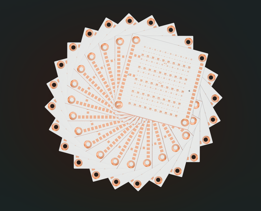

A Direct Thermal Path Copper PCB, also called DTP copper PCB or sinkpad copper base PCB. It is a type of high-performance circuit board used in applications where heat dissipation is critical. Unlike standard printed circuit boards (PCBs), which rely on dielectric layers to insulate the copper circuitry from the metal base, a DTP PCB removes this insulation layer directly beneath the heat-generating components. This creates a direct connection between the component, the copper layer, and the copper base.
This structure allows heat to flow quickly and efficiently away from the source, reducing thermal resistance and improving the performance and reliability of electronic components, especially in high-power or high-current environments. These boards are widely used in LED lighting, automotive systems, telecom infrastructure, and power electronics.
Why Thermal Management Matters in Electronics?
Every electronic device generates heat when itâs running. While small gadgets like phones may only get warm, high-power devices like industrial lighting systems or motor controllers can heat up rapidly. If this heat isnât removed effectively, it can cause serious problems:
Component failure
Reduced lifespan of electronic parts
Malfunction due to overheating
Safety risks, especially in automotive or aerospace applications
To prevent these outcomes, thermal management becomes a critical aspect of PCB design. Engineers use a combination of heat sinks, thermal vias, and copper planesâbut in extreme conditions, these are often not enough. Thatâs where DTP copper PCBs come inâthey allow maximum heat transfer from hot components to the surrounding environment, helping electronics run cooler and more reliably.
Features of DTP Copper PCB
Direct thermal path copper PCBs stand out due to their special construction and capabilities. Here are some of their key features:
Thick copper base (up to 10 oz or more): Helps carry more current and draw heat away quickly.
Direct contact between copper circuit and metal base: Eliminates the thermal barrier of dielectric materials.
Excellent heat dissipation: Thermal resistance is significantly lower compared to regular MCPCBs.
Strong mechanical structure: Supports heavy components without deformation or cracking.
Stable performance in harsh environments: Suitable for high-temperature, vibration, and high-voltage conditions.
These features make DTP PCBs a practical choice for demanding applications where standard PCBs would overheat or fail.
How Does DTP PCB Work?
The principle behind a DTP PCB is simple: remove the thermal barrier (dielectric layer) between the heat source and the metal base. In a typical metal core PCB, the heat generated by a component passes through a dielectric layer (which is an electrical insulator) before reaching the metal base. This dielectric slows down the heat transfer.
In a DTP PCB, the designer removes the dielectric material under the power component and creates a direct copper pad that touches the metal base directly. This structure dramatically reduces thermal resistance and allows heat to flow out much faster.
In short, DTP PCBs give heat a shortcutâa direct path to escapeâleading to lower operating temperatures and better performance.
How Does the Convexity Pad Create?
The convexity pad is a small bump or raised copper structure that connects the top copper circuitry directly to the metal base below. This feature is critical in DTP PCBs because it serves as the contact point for heat transfer. Actually, the convexity pad is a little complicated than normal. Normally the thickness of copper core/substrate is 0.8mm, 1.0mm, 1.2mm, 1.4mm, 1.6mm, 2.0mm. And thereâre blue protection film on both sides. We will remove that protection film after raw material cutting, before convexity making, so that copper can be etched. After that, we will grind the copper core to make sure itâll be clear enough, so that in next step another film can be added to make trace.
Then, we will add one extra layer of film (normally blue color, and will refer to blue film hereafter) on whole area copper core, and after developing & etching, only selected area of blue film will be kept and other area will be removed away. In fact, the area of blue film will be the place convexity will be.
Why Aluminum Base Is Not Suitable to Make DTP PCB?
As we know, the convexity pad directly connects the copper base serving as the substrate to the thermal pads of the LED without any insulating thermal conductive material in between. In this way, the heat from the LED can be directly transferred to the copper substrate of the base through the solder, without having to pass through the electrical traces on the base surface and the insulating materials for heat transfer. This is why DTP PCB also is called thermoelectric isolation as well. (The heat output path of the LED is directly connected to the copper plate and separated from the electrical traces). As for why aluminum substrates cannot be used, it is because the heat pads of the led chips need to be directly soldered to the copper substrate through the solder on the reserved protrusion on the base, and aluminum doesnât bond well with standard solder materials.
In addition to this, some manufacturers said they can make DTP aluminum PCB. Maybe they indeed made it, but need to spend a lot of time and the cost is much higher than DTP copper base PCB. And compared with copper base PCB, the thermal conductivity of aluminum PCB is slightly lower, so we always not recommend customers to make DTP aluminum PCB.
Considerations While Using Direct Thermal Path MCPCB
Before incorporating DTP copper PCBs into your design, keep these factors in mind:
1. Component Placement
Ensure components that generate high heat are directly above the DTP pads. Misalignment can compromise thermal efficiency.
2. Base Thickness
The thickness of the copper base affects both heat transfer and mechanical strength. Heavier bases improve heat conduction but may reduce flexibility.
3. Thermal Simulation
Use thermal analysis software to simulate heat dissipation before production. This helps identify hotspots and optimize layout.
4. Dielectric Material
Where dielectric is still used, choose materials with high thermal conductivity (such as ceramic-filled polymers).
5. Mounting & Enclosure
DTP PCBs perform best when mounted to a heatsink or metal enclosure. Make sure thereâs good thermal interface material between them.
6. Surface Finish
Use finishes like ENIG (Electroless Nickel Immersion Gold) or OSP (Organic Solderability Preservative) to improve soldering and surface protection.
DTP Copper PCB Manufacturing Process
Manufacturing a direct thermal path copper PCB requires careful attention and precision. Here’s a step-by-step breakdown:
Step 1: Base Metal Selection
A thick copper base (typically 1.6â3.2 mm) is chosen as the base layer. This base serves as the thermal sink for the entire board.
Step 2: Lamination
A high-thermal conductivity dielectric is laminated to the copper base. This is done only where insulation is needed.
Step 3: Circuit Layer Preparation
A copper foil (typically 1â3 oz) is applied on top. The PCB manufacturer then performs photolithography and etching to define the circuit pattern.
Step 4: Dielectric Removal
The dielectric under high-heat components is selectively milled or punched to expose the copper base.
Step 5: Convex Pad Formation
Using precision CNC machining, a raised copper pad is formed on the exposed area. This pad directly contacts the component’s thermal pad.
Step 6: Surface Finishing
The board receives a protective finish like ENIG, OSP, or immersion silver to prevent oxidation and improve solderability.
Step 7: Solder Mask and Silkscreen
Solder mask is applied to protect the circuitry, followed by silkscreen for labeling.
Step 8: Testing and Quality Control
Each board undergoes electrical and thermal testing to ensure performance, conductivity, and durability.
This manufacturing process results in a high-performance PCB that can handle extreme heat conditions with ease.
https://www.youtube.com/watch?v=KFQNdAvZGEA
Common Applications of DTP MCPCB
Because of their outstanding heat management, DTP copper PCBs are widely used across industries that rely on high-power or high-brightness components. Here are some key applications:
Automotive LED lighting: Headlights, brake lights, and DRLs require efficient thermal dissipation to maintain brightness and longevity.
Power electronics: DTP PCBs are used in DC/DC converters, motor controllers, and battery management systems for better heat control.
Industrial lighting: High bay and floodlights benefit from improved thermal design to prevent premature failure.
Telecommunication systems: Base stations and network equipment use DTP PCBs to manage heat from amplifiers and processors.
Aerospace and defense: Systems in satellites and aircraft need PCBs that perform reliably under thermal and environmental stress.
Wherever performance and reliability are non-negotiable, DTP copper PCBs are a trusted solution.
FAQs About Direct Thermal Path MCPCB
Q1. What makes DTP PCBs different from regular MCPCBs?
The key difference is the removal of the dielectric layer beneath the component, enabling direct heat flow from the copper pad to the metal base. This dramatically improves thermal conductivity.
Q2. Can DTP copper PCBs be used in multilayer stackups?
Typically, they are single-sided. However, hybrid multilayer configurations are possible for complex applications, though they require advanced design and manufacturing techniques.
Q3. Is copper the only metal used for DTP base material?
In high-end applications, copper is the preferred base due to its superior conductivity and durability. Aluminum is cheaper but less effective in DTP designs.
Q4. Do I still need a heatsink with a DTP PCB?
Yes, in most cases. While the DTP board efficiently moves heat to its base, the heat still needs to exit the boardâoften through a heatsink or the product’s metal housing.
Q5. How can I get a DTP copper PCB made?
Youâll need a PCB manufacturer like EBest Circuit (Best Technology) that specializes in metal core PCBs and has equipment for precision CNC milling and selective dielectric removal. Request thermal simulation support for best results.
Ever wondered why HASL finish PCB remains a cost-effective choice despite its limitations in high-density designs? This guide explores everything from HASL’s solder composition and pitch constraints to manufacturer selection criteria, while addressing thermal risks for heavy copper boards, RoHS compliance trade-offs, and main differences with ENIG finishes.
EBest Circuit (Best Technology)â stands out as your trusted HASL surface finish PCB manufacturer by directly tackling the critical challenges faced by global buyers. We understand the frustrations of inconsistent quality, delayed deliveries, and hidden costs in cross-border procurement. Our HASL finish PCB are manufactured with âIPC-A-600 Class 3 standardsâ, ensuring reliable performance even in demanding environments like automotive and industrial applications. With â15-day standard lead timeâ (30% faster than industry averages) and âcompetitive pricingâ, we eliminate supply chain bottlenecks while keeping your budget intact. Every board undergoes â100% automated AOI testingâ to prevent defects like uneven coating or oxidation. Backed by 10+ years of experience serving EU/NA markets, we offer ââ1 piece MOQ for prototyping, and 24/7 English engineering support to streamline your sourcing process. Letâs turn your PCB procurement from a pain point into a competitive advantage, request a quote today: sales@bestpcbs.com.
What Is HASL Finish PCB?
HASL Finish PCB (Hot Air Solder Leveling) is a common surface treatment for printed circuit boards, where molten solder (typically tin-lead or lead-free alloy) is applied to the copper pads and then leveled using hot air to create a smooth, protective coating. This process prevents oxidation, enhances solderability, and ensures reliable electrical connections during component assembly. While cost-effective and widely used, HASL finish may leave uneven surfaces unsuitable for fine-pitch components, leading to alternatives like ENIG or immersion silver in high-density designs. The method remains popular for general-purpose PCBs due to its durability and ease of inspection.
What Is the Composition of HASL Finish PCB?
Below are the compositions of HASL finish PCB:
Solder Alloy: Solder alloys composed of tin (Sn) and lead (Pb) are mainly used, with a common ratio of 63% tin and 37% lead. However, due to environmental protection requirements and regulatory constraints such as RoHS (Restriction of Hazardous Substances Directive), lead-free solder alloys are now more common. These lead-free alloys are usually made of tin combined with other elements such as silver (Ag), copper (Cu) or bismuth (Bi), which can meet environmental standards and ensure soldering performance.
Flux: Before the printed circuit board (PCB) is immersed in molten solder, the flux needs to be applied to the copper surface. Its main function is to remove oxides and contaminants on the copper surface, improve solder wettability, and enhance adhesion during soldering; at the same time, it can also prevent the copper surface from being oxidized again in subsequent steps, laying the foundation for high-quality soldering.
Copper Substrate: The copper substrate is the basis of the HASL surface treatment PCB and undertakes the conductive function of the PCB. The HASL process is designed to protect the copper substrate from oxidation and corrosion, thereby ensuring the long-term stable operation of the PCB. In addition, the quality and thickness of the copper substrate also have an important impact on the overall performance of the HASL surface-treated PCB. Better copper materials and appropriate thickness can improve electrical performance and mechanical strength.
PCB Base Material: In addition to the copper substrate, the base materials of the PCB (such as epoxy glass fiber boards such as FR-4) are equally important. These materials provide mechanical support and electrical insulation performance. Their quality, heat resistance, and flame retardancy will affect the reliability and service life of the PCB, and are also closely related to the adaptability of the HASL process.
Protective Masking: Protective Masking can cover areas on the PCB that do not require soldering to prevent solder from accumulating in these areas. At the same time, it can further protect the circuit from environmental factors (such as moisture and dust) and improve the stability and durability of the PCB.
What Is the Minimum Pitch for HASL Finish PCB?
The minimum pad pitch for HASL finish PCB is not a fixed value. Generally speaking, it is difficult to achieve a pitch less than 0.5mm for standard HASL processes; in some cases, a well-calibrated HASL process with proper air knife control can achieve a minimum pitch of about 0.4mm.
Factors affecting pad pitch and solutions
Component – Dependent
Impact: The minimum pitch for HASL surface finish PCBs depends largely on the components used. Larger through-hole components can have relatively wide pitches; however, fine-pitch surface mount components pose challenges for the HASL process.
Solution: Choose the appropriate process based on the component type. For fine-pitch surface mount components, other more suitable surface finishes can be considered; if the HASL process must be used, communicate with the manufacturer in advance to optimize the process.
Process Variables
Impact: Variables in the HASL process itself affect the minimum achievable pitch. The air knife angle and pressure used to level the solder are critical. Non-optimal air knife settings can result in uneven solder distribution and bridges between fine-pitch pads.
Solution: Accurately calibrate the HASL process, tightly control air knife parameters, and perform multiple trials to find the optimal air knife angle and pressure settings to ensure uniform solder distribution.
Solder Alloy Characteristics
Impact: The type of solder alloy used affects the minimum pitch. Lead-free solder alloys have different melting points and flow characteristics than traditional tin-lead alloys, requiring more precise control in the HASL process to achieve fine pitch. Some lead-free alloys are better suited for slightly coarser pitches, while others can be used for finer pitches after careful process adjustments.
Solution: Choose the solder alloy appropriately based on the minimum pad spacing required. Perform process testing and adjust process parameters to suit the alloy characteristics before using a new alloy material.
How to Choose A Good HASL Surface Finish PCB Manufacturer?
Hidden Costs: Clarify testing, tooling, and rush fees.
Panelization: Choose manufacturers offering panelized production (reduces unit cost by 15â25%).
Why Does HASL Finish Cause Uneven Surfaces on Fine-Pitch PCBs?
Solder Flow: In fine-pitch areas, narrow pad gaps and solder surface tension can cause uneven flow, leading to bridging between pads.
Air Knife: Inconsistent air pressure or suboptimal angles across the PCB surface, especially in fine-pitch regions, can leave excess solder unevenly.
Thermal Changes: Rapid heating and cooling during HASL can cause differential expansion and contraction in fine-pitch areas, warping the solder.
Flux Residue: Unremoved flux residue acts as a barrier, causing uneven solder adhesion in fine-pitch areas.
Complex Design: Boards with many fine-pitch components, multiple layers, and vias disrupt solder flow, making uniform finishes hard to achieve.
Solder Alloy: Some alloys, particularly lead-free ones with high viscosity, struggle to flow smoothly in fine-pitch gaps.
Process Variations: Minor fluctuations in temperature, solder bath composition, or conveyor speed accumulate and affect fine-pitch PCB surface quality.
Can Your HASL Manufacturer Prevent Thermal Damage to Heavy Copper PCBs?
Yes, EBest Circuit (Best Technology) has taken a series of strict and effective measures to prevent heavy copper PCBs from thermal damage during the HASL process. The specific implementation measures are as follows:
Preheating Optimization: For heavy copper PCBs, EBest Circuit (Best Technology) will carefully optimize the preheating step. Before immersing the PCB in the molten solder bath, its temperature is gradually increased to reduce thermal shock. The preheating process is adjusted according to the thickness and copper content of the heavy copper PCB to ensure a more controlled temperature transition.
Solder Bath Temperature Control: It is crucial to maintain accurate and stable solder bath temperature. EBest Circuit (Best Technology) is equipped with an advanced temperature control system that can accurately adjust the temperature of the molten solder to prevent the heavy copper PCB from overheating and causing thermal damage.
Cooling Rate Management: After the HASL process is completed, the cooling rate of the heavy copper PCB is also critical. EBest Circuit (Best Technology) will use a suitable cooling system such as forced air cooling or temperature-controlled cooling chamber to control the cooling rate, slow down the cooling process, reduce the stress on the PCB, and avoid thermal damage caused by sudden temperature changes.
Process Monitoring and Adjustment: Continuous monitoring of HASL process parameters is essential. EBest Circuit (Best Technology) deploys sensors and monitoring equipment to track variables such as temperature, air pressure, and conveyor speed in real time. Once any deviation is detected, the process is adjusted quickly to prevent thermal damage to heavy copper PCBs.
Use of Thermal Protection Materials: In some cases, EBest Circuit (Best Technology) uses thermal protection materials or coatings on heavy copper PCBs before the HASL process. These materials help to dissipate heat more evenly and protect the PCB from excessive thermal stress.
Customized Process Recipes: For heavy copper PCBs, EBest Circuit (Best Technology) develops customized HASL process recipes. These recipes take into account the specific characteristics of heavy copper PCBs such as copper thickness, number of layers, and board size to optimize the process and minimize the risk of thermal damage.
Training and Expertise of Operators: Well-trained operators are key to preventing thermal damage. EBest Circuit (Best Technology)’s operators are familiar with the special requirements of heavy copper PCBs and can make real-time adjustments to the HASL process as needed. At the same time, the company conducts regular training and updates the latest technical knowledge to enhance the ability of operators to handle heavy copper PCB production.
Testing and Validation: Before mass production of heavy copper PCBs with HASL surface treatment, EBest Circuit (Best Technology) conducts comprehensive testing and validation, including thermal cycle testing to simulate actual working conditions to ensure that the PCBs can withstand the thermal stress of the HASL process without damage.
Is Your HASL Finish RoHS-Compliant Without Sacrificing Solderability?
Preheating Optimization: A good HASL manufacturer will carefully optimize the preheating step for heavy copper PCBs. By gradually raising the temperature of the PCB before immersion in the molten solder bath, it helps to reduce thermal shock. This preheating process can be adjusted based on the thickness and copper content of the heavy copper PCB to ensure a more controlled temperature transition.â
Solder Bath Temperature Control: Maintaining a precise and stable temperature in the solder bath is crucial. The manufacturer should have advanced temperature control systems that can accurately regulate the temperature of the molten solder. This helps to prevent overheating of the heavy copper PCB, which could lead to thermal damage.â
Cooling Rate Management: After the HASL process, the rate at which the heavy copper PCB cools is also important. A proper cooling system, such as forced – air cooling or a controlled – temperature cooling chamber, can be used to manage the cooling rate. Slowing down the cooling process can reduce the stress on the PCB and prevent thermal damage caused by rapid temperature changes.â
Process Monitoring and Adjustment: Continuous monitoring of the HASL process parameters is essential. The manufacturer should have sensors and monitoring equipment to track variables such as temperature, air pressure, and conveyor speed. If any deviations are detected, the process can be quickly adjusted to prevent thermal damage to the heavy copper PCB.â
Use of Thermal Protection Materials: In some cases, the manufacturer may use thermal protection materials or coatings on the heavy copper PCB before the HASL process. These materials can help to dissipate heat more evenly and protect the PCB from excessive thermal stress.â
Customized Process Recipes: For heavy copper PCBs, a manufacturer may develop customized HASL process recipes. These recipes take into account the specific characteristics of the heavy copper PCB, such as copper thickness, layer count, and board size, to optimize the process and minimize the risk of thermal damage.â
Training and Expertise of Operators: Well – trained operators are key to preventing thermal damage. The operators should be knowledgeable about the unique requirements of heavy copper PCBs and be able to make real – time adjustments to the HASL process as needed. Regular training and updates on the latest techniques can enhance their ability to handle heavy copper PCB production.â
Testing and Validation: Before mass – producing heavy copper PCBs with HASL finish, the manufacturer should conduct thorough testing and validation. This includes thermal cycling tests to simulate real – world operating conditions and ensure that the PCB can withstand the thermal stresses of the HASL process without damage.
What Is the Difference Between ENIG and HASL Finish PCB?
Here are difference between ENIG and HASL finish PCB:
Surface Finish Appearance
HASL: Rough, uneven surface; traditional tin-lead HASL has non-uniform texture, lead-free may be matte.
ENIG: Smooth, shiny surface with uniform nickel layer and reflective gold top layer.
Solderability
HASL: Excellent; easily re-melted, reliable for soldering.
ENIG: Good, but thick gold or nickel-gold interface issues can cause problems like “black pad”.
Cost
HASL: Cost-effective; simple equipment and materials, lower alloy cost.
HASL: Some protection, but solder can oxidize in harsh conditions.
ENIG: Better; nickel barrier and oxidation-resistant gold layer.
Compatibility with Components
HASL: Good with most components, challenges with fine-pitch due to uneven surface.
ENIG: Highly compatible with all component sizes, smooth surface aids precision.
Process Complexity
HASL: Straightforward; dip in solder bath, level with air knives.
ENIG: Complex; multiple steps, strict control of temperature, chemicals, and time.
Shelf Life
HASL: Decent; stable but may oxidize in humidity.
ENIG: Good; stable gold layer, maintains quality in proper storage.
Conclusion
In conclusion, through this blog, we’ve explored what HASL finish PCB is, its composition, minimum pitch capabilities, how to choose a reliable HASL finish PCB manufacturer, reasons for uneven surfaces on fine-pitch PCBs, prevention of thermal damage to heavy copper PCBs, RoHS compliance, and the differences between HASL and ENIG finishes. If you’re looking for high quality HASL finish PCB, please don’t hesitate to reach out to us at sales@bestpcbs.com for a quote. Looking forward to hearing from you!
HDI printed circuit board is at the core of todayâs compact, powerful, and high-speed electronics. If your product needs faster signals, tighter space, and better reliability, HDI technology is the smart choice.
EBest Circuit (Best Technology) is committed to providing HDI printed circuit board prototypes, HDI PCB design, and assembly to all walks of life. We help clients avoid rework by offering DFM reviews early. With our in-house testing, traceability via MES, and certifications like ISO 13485, IATF 16949, and AS9100D, we meet medical, auto, and aerospace needs. Plus, we keep the consistency of quality and prompt delivery. If any HDI printed circuit board cases need us to help, just kindly contact us at sales@bestpcbs.com anytime.
What is a HDI Printed Circuit Board?
HDI, short for High-Density Interconnect, is a type of PCB that features finer lines and spaces, smaller vias, and higher connection pad density. Itâs made for advanced designs where every millimeter matters. Unlike standard boards, it can carry more components in less space, helping devices stay sleek yet powerful.
What is the Difference Between HDI PCB and Normal PCB?
Standard PCBs are good for basic layouts, but HDI PCBs offer more layers and tighter designs. Normal PCBs use through-hole vias. HDI boards use microvias, blind vias, and buried vias. This change cuts noise, boosts speed, and reduces size. For high-frequency or multi-functional applications, HDI outperforms standard boards easily.
What is the HDI Layout?
An HDI layout uses small vias and tight routing to pack more functionality into each layer. Designers need to consider signal integrity, heat paths, and high-speed rules. With fine trace widths below 75ÎŒm and via-in-pad structures, HDI layouts allow smartphones, medical tools, and automotive modules to do more in less space.
How Many Layers Can a Printed Circuit Board Have?
In general, PCBs can have 2 to over 20 layers. For HDI printed circuit boards, the layer count often ranges from 4 to 12, depending on how many build-up layers and via combinations are used. Complex HDI stacks with multiple sequential laminations offer unmatched performance in small packages.
How to Do the HDI PCB Design?
Designing HDI requires early coordination with the PCB manufacturer. First, follow the HDI PCB design guide PDF to understand manufacturing limits. Use tools that support blind/buried via planning, differential pair spacing, and impedance control. Simulate DFM early and apply rules like the 3W spacing rule to cut cross-talk. At EBest Circuit (Best Technology), we review your layout with CAM teams early to reduce back-and-forth and shorten design time.
How Does a HDI Printed Circuit Board Work?
HDI boards connect dense components using microvias and stacked structures. Tiny holes link each layer with tight precision, sometimes within 3ÎŒm tolerance. Signals travel through controlled-impedance paths, staying clean even at high frequencies. With embedded parts and advanced plating, these boards function faster, cooler, and more reliably.
What Are the Advantages of Printed Circuit Board?
Printed circuit boards give electrical stability, compact form, and ease of mass production. With HDI upgrades, they also give you stronger signal performance, better thermal paths, and increased routing space. You can fit more IOs, more power control, and faster processingâall on a smaller footprint.
What is HDI Printed Circuit Board Used For?
Youâll find HDI PCBs in smartphones, cameras, medical gear, servers, and automotive radar systems. Anywhere size, speed, and reliability matter, these boards lead the way. They are also essential in HDI electronics like wearables, military tech, and 5G communication.
In summary, choosing an HDI printed circuit board isnât just a technical decisionâitâs a strategic one. Whether you need better signal routing, smaller layouts, or faster thermal relief, HDI gives you an edge. As a tech-driven HDI PCB Manufacturer, EBest Circuit (Best Technology) backs that up with smart design help, better materials, and prompt delivery. A warm welcome to contact us at sales@bestpcbs.com for any HDI PCB design needs.
IMS PCB stands for Insulated Metal Substrate Printed Circuit Board. Itâs a specialized type of PCB designed to manage heat more effectively than standard boards. At its core, an IMS board is made of three main layers: a metal base (usually aluminum), a thermally conductive dielectric layer, and a copper circuit layer on top.
This unique construction gives IMS boards exceptional heat transfer capabilities. Unlike standard FR4 boards, where heat may accumulate and degrade performance over time, an IMS PCB actively channels heat away from components and dissipates it through the metal base. This process helps protect sensitive parts and improves overall device longevity.
IMS PCBs are commonly used in LED lighting systems, power converters, automotive electronics, solar inverters, and industrial control systems. Any circuit that generates significant heat can benefit from the enhanced thermal management of an IMS PCB.
Features of IMS PCB
IMS PCBs are favored in demanding applications because of their distinct advantages. Below are some of the standout features:
1. The dielectric layer in an IMS PCB has much higher thermal conductivity compared to FR4.
2. Once heat reaches the metal base, it is dispersed across a larger surface area or transferred to a heatsink.
3. The metal base not only helps with heat but also strengthens the board. This added rigidity reduces the chances of warping, especially in environments with temperature cycling or mechanical stress.
4. Components perform better and last longer when they remain within optimal temperature ranges.
5. Most IMS boards are single-sided, simplifying the layout and making them easier to manufacture. However, advanced designs may include multilayer configurations when required.
6. The metal base can also serve as a shield against EMI interference, which is useful in sensitive analog or RF applications.
Types of IMS Boards
Different IMS boards are used for different applications depending on the metal type and overall construction. Here are the three primary types:
Aluminum-Based IMS PCB
This is the most popular type and often the first choice for LED lighting and consumer electronics. Aluminum is lightweight, affordable, and has decent thermal performance. It strikes a balance between cost and functionality for a wide range of applications.
Copper-Based IMS PCB
Copper has better thermal and electrical conductivity than aluminum. These boards are used in high-end applications where superior thermal management is critical, such as power modules, solar inverters, and automotive control systems. However, copper is more expensive and heavier than aluminum.
Steel-Based IMS PCB
Less common but useful in environments where mechanical durability is crucial. Steel doesnât conduct heat as efficiently as copper or aluminum but provides maximum rigidity and resistance to deformation. Itâs mainly used in industrial or military electronics.
Each type of IMS PCB is selected based on the specific needs of your project. Aluminum offers a good starting point, copper pushes performance higher, and steel provides strength for the harshest conditions.
IMS PCB Stack-up
A critical element in IMS board design is the stack-up, which refers to how the different layers of the board are arranged. The typical IMS PCB stack-up includes the following:
1. Copper Layer
This is where all the electronic traces and pads are formed. The copper thickness usually ranges from 1 oz to 3 oz per square foot, depending on current requirements. It serves as the pathway for electrical signals and power.
2. Dielectric Layer
This is the thermally conductive but electrically insulating layer that separates the copper and the metal base. Itâs usually made of a polymer filled with ceramic particles. The dielectric plays a vital role in transferring heat efficiently while preventing short circuits. The thickness typically ranges from 0.075 mm to 0.2 mm, with thermal conductivity from 1 to 7 W/m·K, depending on material grade.
3. Metal Base
This is typically made of aluminum, copper, or steel. The metal provides mechanical support and acts as the main heat dissipation path. Its thickness usually ranges from 1 mm to 2 mm, but thicker bases are used in heavy-duty applications.
Some advanced designs may include additional dielectric and copper layers to create double-layer or multilayer IMS PCBs, though this increases cost and complexity.
How Thick is an IMS PCB?
The total thickness of an IMS PCB is influenced by the materials used and application requirements. On average, the board thickness ranges from 0.8 mm to 3.2 mm, but custom configurations are available.
Hereâs a breakdown of each layerâs contribution to overall thickness:
Copper Layer: 35â105 ”m (1â3 oz)
Dielectric Layer: 75â200 ”m
Metal Base Layer: 1.0â2.0 mm (for aluminum or copper)
Applications requiring high current typically demand thicker copper layers and sometimes thicker base metals. Likewise, if better insulation is needed, the dielectric layer can be made thicker, but this may reduce heat transfer efficiency. Engineers must balance electrical, thermal, and mechanical requirements to define the most suitable thickness.
What is the Difference Between IMS PCB and FR4 PCB?
Though both are used in electronic devices, the differences between IMS PCB and FR4 PCB are quite substantial:
Parameter
IMS PCB
FR4 PCB
Full Name
Insulated Metal Substrate PCB
Flame Retardant Grade 4 PCB
Base Material
Metal core (usually aluminum or copper)
Fiberglass-reinforced epoxy (FR4)
Thermal Conductivity
High (1â7 W/m·K, depending on dielectric)
Low (typically 0.3â0.4 W/m·K)
Heat Dissipation
Excellent, through metal base
Limited, requires heatsinks or fans
Layer Structure
Usually single-sided
Can be single, double, or multilayer
Mechanical Strength
High (due to metal base)
Moderate (flexible but less rigid)
Weight
Heavier (due to metal core)
Lighter
Manufacturing Cost
Higher
Lower
Applications
Power electronics, LEDs, automotive, solar
Consumer electronics, IoT, communication devices
Thermal Resistance
Low (better heat flow)
High (poor thermal path)
Electrical Insulation
Through thermally conductive dielectric
Provided by FR4 material itself
Common Copper Thickness
1â3 oz
1â2 oz
Typical Board Thickness
0.8â3.2 mm
0.6â2.0 mm
Design Complexity
Lower (usually single-layer)
Higher (multilayer and complex routing possible)
Price Range
Mid to High
Low to Mid
What is the Thermal Resistance of IMS Board?
Thermal resistance (RΞ) refers to a materialâs resistance to heat flow. In IMS PCBs, it is mainly influenced by the dielectric layer. A lower RΞ means better heat transfer and lower temperature rise.
The thermal resistance of an IMS board is calculated using:
RΞ = t / (k à A)
Where:
t = dielectric thickness
k = thermal conductivity
A = surface area
Typical values for IMS PCBs range from 0.2°C/W to 1.0°C/W, depending on materials and layout. Advanced dielectric materials with high k-values can push this number lower, helping improve performance in high-power applications.
Designers often select materials with k ℠3 W/m·K and limit the dielectric layer to under 150 ”m to achieve low thermal resistance.
If you’re sourcing IMS PCBs and want consistent quality, EBest Circuit (Best Technology) is your go-to IMS PCB manufacturer. We have a dedicated production line for metal-core PCBs, including aluminum, copper, and hybrid metal boards.
Why Choose EBest Circuit (Best Technology)?
✅ Professional Engineering Support: Our experienced team helps optimize stackups, select dielectric materials, and improve thermal paths in your layout.
✅ ISO Certifications: We are certified with ISO9001, IATF16949, ISO13485, and AS9100D, serving a wide range of industries including medical, automotive, and aerospace.
✅ MES Traceability: Every board is tracked using our MES system to ensure complete traceability from raw materials to final shipment.
✅ Flexible Volumes: Whether you need a prototype batch or full-scale production, we offer scalable solutions.
✅ Comprehensive IMS PCB Assembly: Beyond PCB fabrication, we also offer full assembly including component sourcing, reflow soldering, inspection, and testing.
From concept to finished product, we work closely with clients to deliver high-performance IMS PCBs that meet electrical, mechanical, and thermal demands.
FAQs
1. What does IMS PCB stand for?
It stands for Insulated Metal Substrate Printed Circuit Board, a high-performance board for heat-sensitive applications.
2. Can IMS PCB be double-sided?
Yes, though less common. Double-sided IMS PCBs require more advanced fabrication and cost more, but theyâre available for complex designs.
3. Is IMS PCB good for automotive systems?
Absolutely. Automotive systems generate a lot of heat and require reliability. IMS PCBs are ideal for ECUs, power converters, and headlight controls.
4. What thermal conductivity should I choose for my dielectric layer?
It depends on the heat generated. For moderate power, 1â2 W/m·K is enough. For high-power LEDs or power modules, choose â„3 W/m·K.
5. How do I request a quote from EBest Circuit (Best Technology)?
Send your Gerber files, stackup requirements, and assembly needs to our team, and weâll respond with a customized quote within 24 hours.
This website uses cookies to enhance your experience, remember your preferences, and help us understand how visitors use our site. You can accept all cookies, reject non-essential cookies, or manage your settings.
This website uses cookies to improve your experience while you navigate through the website. Out of these cookies, the cookies that are categorized as necessary are stored on your browser as they are essential for the working of basic functionalities of the website. We also use third-party cookies that help us analyze and understand how you use this website. These cookies will be stored in your browser only with your consent. You also have the option to opt-out of these cookies. But opting out of some of these cookies may have an effect on your browsing experience.
Necessary cookies are absolutely essential for the website to function properly. These cookies ensure basic functionalities and security features of the website, anonymously.
Cookie
Duration
Description
cookielawinfo-checkbox-analytics
11 months
This cookie is set by GDPR Cookie Consent plugin. The cookie is used to store the user consent for the cookies in the category "Analytics".
cookielawinfo-checkbox-functional
11 months
The cookie is set by GDPR cookie consent to record the user consent for the cookies in the category "Functional".
cookielawinfo-checkbox-necessary
11 months
This cookie is set by GDPR Cookie Consent plugin. The cookies is used to store the user consent for the cookies in the category "Necessary".
cookielawinfo-checkbox-others
11 months
This cookie is set by GDPR Cookie Consent plugin. The cookie is used to store the user consent for the cookies in the category "Other.
cookielawinfo-checkbox-performance
11 months
This cookie is set by GDPR Cookie Consent plugin. The cookie is used to store the user consent for the cookies in the category "Performance".
viewed_cookie_policy
11 months
The cookie is set by the GDPR Cookie Consent plugin and is used to store whether or not user has consented to the use of cookies. It does not store any personal data.
Functional cookies help to perform certain functionalities like sharing the content of the website on social media platforms, collect feedbacks, and other third-party features.
Performance cookies are used to understand and analyze the key performance indexes of the website which helps in delivering a better user experience for the visitors.
Analytical cookies are used to understand how visitors interact with the website. These cookies help provide information on metrics the number of visitors, bounce rate, traffic source, etc.
Advertisement cookies are used to provide visitors with relevant ads and marketing campaigns. These cookies track visitors across websites and collect information to provide customized ads.