A shared oval antipad can reduce local capacitance in a differential via transition, but it also removes plane copper. Compare it with two separate openings in the actual stackup. Keep the signal pair, return vias and fabrication clearances in the model rather than enlarging the cutout by itself.
What an Antipad Does
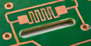
An antipad is a clearance in copper around a feature that must not connect to that copper. At a signal via, it also changes the electrical coupling between the via and the reference plane. Texas Instruments’ differential via article discusses those effects and a shared oval example.
Why Two Openings Are Not the Same as One
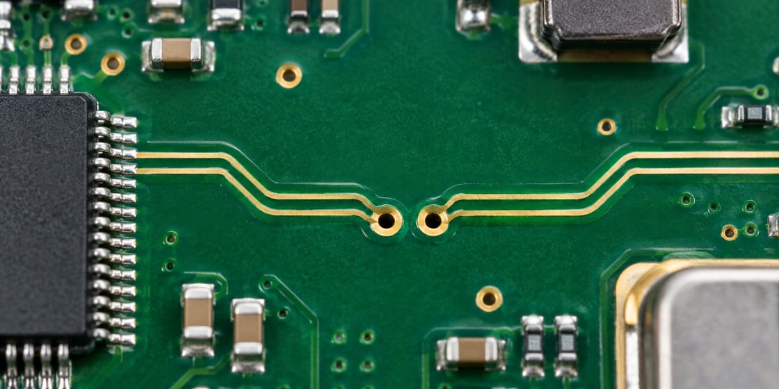
Two separate clearances can leave a copper bridge between them. A shared opening removes that bridge and changes the field around both vias. Neither arrangement is universally better; compare the transition and surrounding reference structure.
Detailed Model Inputs
| Input | Unit or record | Purpose |
| Via pitch | mm | Sets pair spacing |
| Pad and barrel | Finished geometry | Defines the conductor |
| Opening by layer | Shape and dimensions | Describes plane clearance |
| Return vias | Position and reference net | Represents the return path |
| Stub and layer pair | Length and layer IDs | Describes the transition |
Shared Oval vs Separate Antipads
| Feature | Separate openings | Shared opening |
| Plane between the vias | May retain copper | Removed in the shared region |
| Electrical review | Coupling with retained bridge | Coupling with common opening |
| Fabrication review | Width and stability of copper web | Clearance to nearby features |
Worked Example: Check Whether a Web Remains
For two aligned circular openings of 0.45 mm diameter with centres 0.55 mm apart, their nominal edge separation is 0.10 mm. That is only the artwork value for this hypothetical case. Verify the intended finished web and tolerance or compare a shared opening instead.
Keep Both Sides of the Pair Comparable
Review symmetry around each via, the nearby reference connections and any asymmetry introduced by other routing. An electrically asymmetric environment can affect the differential transition. Do not judge the pair only by whether its two hole sizes match.
Do Not Remove Return Copper Without Checking the Path
A larger opening can clear copper around the signal vias but also reshape the nearby reference region. Review where return current can transfer between planes. If a neighbouring path becomes narrow or interrupted, assess that change as part of the same comparison.
Model the Stub and Pads With the Opening
The pad, barrel, stub and antipad contribute to one transition. A short local impedance change is not automatically attributable to the opening. Keep the geometry consistent between alternatives and use an appropriate model when the bandwidth or loss budget makes the distinction important.
Review Layer-Specific Clearance
The same opening is not necessarily appropriate on every layer. Check plane assignments, copper features and any controlled-depth operation. For the broader treatment of unused barrel, see the BestPCBs via stub guide.
Compare an Actual Test Structure
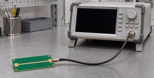
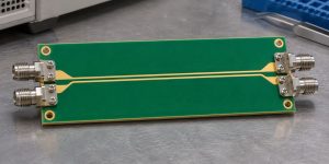
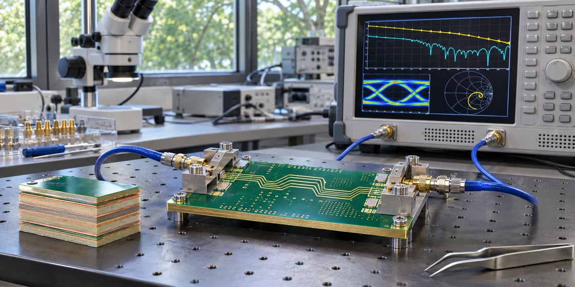
For a sensitive link, use a structure that reproduces the layer change, openings, nearby grounds and routing. A straight impedance coupon alone cannot demonstrate the transition. Agree on the test objective and how fixture effects will be interpreted.
Keep the Fabricator’s Clearance Rules Separate
The model answers an electrical question; the fabricator confirms which openings and copper features can be built. Check the artwork, layer-by-layer clearances and applicable tolerances. If the final geometry changes, rerun the relevant comparison before accepting the build.
Record the Selected Geometry and Evidence
Keep the via dimensions, opening shape, layer map, return arrangement and verification result together. Record why the selected option met the actual requirements. If the stackup changes, revisit the transition instead of assuming an old clearance is still appropriate.
Discuss a High-Speed Stackup
Share the layer pair and via geometry with Best Technology.
FAQ
Is a shared oval antipad always better?
No. A shared opening changes capacitance and also removes plane copper between the vias. The right choice depends on the stackup, return paths, dimensions and electrical target. Compare both options and verify the fabrication constraints instead of adopting the oval solely because a reference design used it.
What if two separate openings overlap?
Then they no longer preserve a complete web between them in the overlapping area. Review the actual resulting shape rather than treating the artwork as two independent circles. Confirm the intended clearance with the fabricator and use the correct merged geometry in any electrical model.
Is the antipad the same as the via pad?
No. The via pad is a conductor intended to connect at an applicable layer. The antipad is an opening in surrounding copper where a connection is not intended. Identify both on the relevant layer so their sizes and purposes are not accidentally swapped.
Can I enlarge the antipad to fix any impedance dip?
Not reliably. A dip can involve multiple parts of the transition, and changing the opening may affect return geometry or nearby features. Compare the suspected mechanism with a suitable model or measurement before changing the layout, and check the impact on the rest of the path.
Do return vias still matter for a differential pair?
Yes, evaluate them as part of the actual reference transition. Differential signals interact with nearby copper, and asymmetry or a reference change can matter. Confirm where the references connect and model the geometry that will be built rather than assuming the pair needs no return review.
Will a standard impedance coupon show the effect?
Only if the coupon includes a representative transition and the method can resolve it. A straight uniform trace checks a different structure. If the antipad decision is important, specify the relevant layer change and geometry and agree how the result will be interpreted.
Can different layers use different antipad shapes?
They can be designed differently when the electrical and manufacturing requirements support it. Check the relevant plane, clearance and nearby geometry on each layer. Document the actual shapes for the model and fabrication release rather than relying on a single label for the entire via.
What should I send for a transition review?
Send the stackup, via pitch, pad and barrel dimensions, layer-specific openings, return-via positions and stub details. Include the interface requirements and intended measurement or simulation scope. Those inputs let the reviewer assess the transition without guessing what the clearance drawing means.