A PCB screw terminal joins a field wire to a circuit board through a screw-clamped contact and soldered or surface-mounted board interface. A reliable connection requires more than matching the pin pitch: the finished hole must fit the actual lead, the pad must retain enough copper around that hole, the chosen conductor must fit the clamp, and the enclosure must leave room to insert the wire and tighten the screw without levering the board. At EBest Circuit (Best Technology), we review these interfaces when preparing a board and assembly for a specified terminal.

What Is a PCB Screw Terminal?
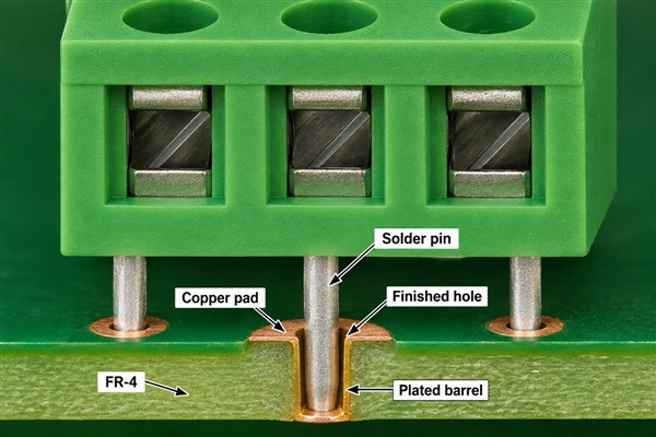
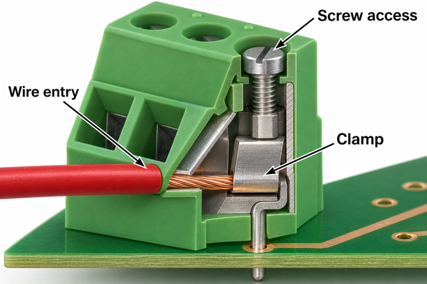
A board-mounted screw terminal is a wire-to-board interface: a screw or clamp grips the conductor inside an insulating housing, while separate contacts connect to the PCB. The screw does not fasten the PCB itself. In a through-hole version, each contact has a solder pin inserted into a plated hole. In a surface-mount version, metal terminations attach to lands on the board. First identify the exact manufacturer part number, because visually similar housings can have different footprints, wire ranges, access angles and torque limits.
Which PCB Mounting Style Fits the Assembly?
Through-hole screw terminal blocks are a common choice where the terminal is hand-wired after assembly. The plated holes and solder fillets connect the contact pins electrically, but the finished product still needs mechanical support for wiring operations. Surface-mount terminals use a different land pattern and must be selected only where the connector maker permits that mounting and the assembly process can control its loading. A pluggable system separates the soldered board header from the wire-clamping plug; it changes service access but does not remove the need to verify both halves of the mating pair.
How Do Pitch and Position Count Affect the Footprint?
Pitch is the center-to-center spacing between neighboring contacts, not the outside width of the housing. Position count determines the number of electrical connections and the total row length. A 3-position block with 5.08 mm pitch has two pitch intervals between its first and last contact centers; housing overhang adds further width. Use the manufacturer’s drilling plan to place pins, not a ruler measurement of the plastic body. Check that adjacent wire ports, labels and enclosure openings remain accessible at the final position count.
How Should You Size PCB Screw Terminal Holes?
Start with the recommended PCB hole diameter for the exact part, then agree whether the drawing calls out a finished plated-hole diameter or a drill size. Plating reduces the opening after drilling; the fabrication drawing must communicate which value governs fit. For example, Phoenix Contact specifies a 1.4 mm PCB hole for its SMKDS 2,5/3-5,08, part 1705472, whose rectangular pin is 1.0 x 0.9 mm. A rectangular pin cannot be checked against a round hole by comparing only its 1.0 mm side with the hole diameter: the ideal sharp-corner diagonal is sqrt(1.0² + 0.9²), or about 1.345 mm. That leaves only about 0.055 mm between this geometric envelope and the listed 1.4 mm hole before actual pin corner form and dimensional variation are considered.
For a conditional screening example, if the project defines 1.4 mm as the target finished plated hole and our published standard PTH tolerance of ±0.075 mm applies, the lower finished-hole limit would be 1.325 mm. That is smaller than the sharp-corner diagonal above; it does not prove the maker’s recommended footprint is wrong, because actual pin corners, tolerances and the maker’s hole-diameter basis still need confirmation. Send the exact pin drawing and hole callout to the PCB fabricator, agree the finished-hole limits and test insertion on a production-intent board. Do not substitute this arithmetic for the connector maker’s qualified land pattern.
How Large Should the Pads and Annular Rings Be?
The hole alone does not define a manufacturable footprint. The pad needs an annular ring after finished-hole variation and drill-to-copper registration, while preserving clearance to neighboring copper. We check the supplied footprint against our FR-4 PCB fabrication process and the specific board stack-up. If the connector maker provides a land pattern, start there. The following calculation shows how to review a candidate pad; it is not a universal terminal footprint or a guaranteed production combination.
Suppose the drawing proposes a 1.8 mm pad and specifies a 1.4 mm target finished PTH. With our published standard ±0.075 mm PTH diameter tolerance, the largest opening would be 1.475 mm. Its concentric copper ring would then be (1.8 – 1.475) / 2 = 0.1625 mm. If the applicable minimum finished ring is 0.075 mm, only 0.0875 mm remains for the combined radial loss from registration and copper-edge variation. The published hole-position figure is not automatically a drill-to-copper registration allowance; we must confirm that allowance, the finished pad size, adjacent-pad clearance and the connector housing against the actual fabrication drawing before accepting the candidate.
| Footprint input | Take it from | Check on the finished board |
|---|---|---|
| Pin size and shape | Exact terminal drawing | Clearance through the plated opening |
| Recommended hole | Exact terminal drilling plan | Finished-hole tolerance and plating |
| Pad diameter | Connector land pattern and board DFM | Minimum annular ring after registration |
| Pitch and polarity | Part drawing and circuit netlist | Contact spacing and pin-1 orientation |
| Board edge distance | Mechanical assembly drawing | Housing overhang, routing and support |
How Should Copper Reach the Terminal Pads?
Route the current path from each pad into copper sized for the actual load, temperature rise and finished copper thickness. A terminal’s catalog current rating is not a rating for the PCB trace that feeds it. Avoid a narrow neck at a high-current pad unless it is intentionally designed and validated. Keep solder-mask openings, adjacent-net spacing and creepage appropriate to the product voltage and environment. Our two-layer PCB fabrication can support a simple terminal interface, but the actual current path and insulation requirements must be designed for the project rather than inferred from the number of layers.
Which Wire Gauge and Ferrule Fit the Clamp?
Select the conductor from the exact terminal’s approved cross-section range and conductor type, then check current, insulation diameter and cable temperature rating separately. Solid wire, fine-stranded wire, bare stranded wire and ferruled wire do not always share the same permitted range. For the Phoenix Contact example above, the published rigid and flexible conductor range is 0.14-2.5 mm² (AWG 26-14); ferruled flexible conductor range is 0.25-2.5 mm². Its specified stripping length is 11 mm. The ferrule, if used, must also fit the actual clamp and be crimped for the selected conductor, not merely match the nominal AWG on a purchasing list.
How Does Wire-Entry Direction Change Placement?
Wire entry can be horizontal, vertical or angled relative to the PCB. That orientation determines where the cable approaches the housing and whether it can bend without loading the clamp or board. The cited SMKDS 2,5/3-5,08 has a 50-degree wire entry. To check a replacement, first compare the pin coordinates, shape, finished holes and body keepout for PCB footprint compatibility. Then compare the wire approach, housing, enclosure opening and tool access for installed-product compatibility. A different entry angle does not by itself prove that the PCB holes are incompatible; matching PCB holes do not prove that the wired product fits its enclosure.
How Much Screwdriver Clearance Is Needed?
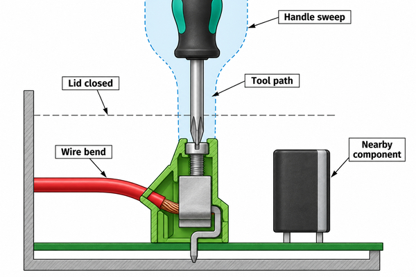
Place the board in its installed position and draw the intended screwdriver bit and handle above each screw. Trace the shaft’s insertion path, the space the handle occupies while it is turned, and the cable bend beside the tool. In the side-view check below, the lid is removed for tool access; its dashed closed position crosses the tool envelope. Resolve that interference in the actual product layout rather than copying a made-up clearance dimension. Check the first and last terminal positions, the nearest tall component and the real assembly sequence with the specified tool. If the lid must be removed for wiring, state that sequence in the work instruction rather than assuming access through a narrow slot.
What Happens to the PCB When a Screw Is Tightened?
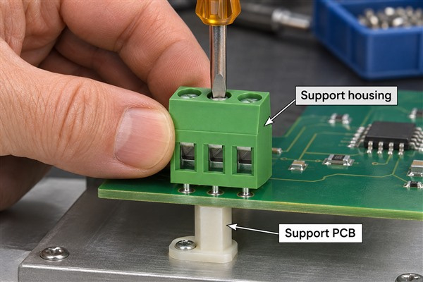
Torque applied at the screw can push or twist the terminal housing; wire insertion and pull can add further loads. Those loads can travel through solder pins, plated barrels, pads and the laminate if the housing is left unsupported. Phoenix Contact specifically warns that, for two- or three-position blocks with one solder pin per contact, those individual pins cannot compensate for the connection force. The manufacturer calls for support of the terminal housing while the conductor is connected. Its example model specifies 0.5-0.6 N·m tightening torque; that value is not a universal screw-terminal setting.
How Can You Support the Terminal and the Board?
Provide board mounting points or a fixture close enough to limit bending during wiring, and support the terminal housing when the screw is tightened. The housing support must resist the tool load without pressing on the conductor or using solder joints as mechanical stops. Route the cable to an enclosure clamp or strain-relief feature where the product requires one. A cable tie far from the entry does not necessarily stop leverage at the terminal. We can review the board’s mounting-hole and terminal-pad placement against the customer’s enclosure drawing, while the enclosure and field-wiring method remain part of the complete product design.
What Should Be Inspected After Soldering?
Inspect each pin for correct seating, orientation and an acceptable solder joint on the specified side of the board. Also check for solder bridges, housing damage and flux residue where it matters to the product. A continuity check can detect an open net, but it cannot by itself show that the solder joint survived mechanical loading or that a wire is clamped correctly. In our PCB assembly work, the accepted inspection and test method should be tied to the customer drawing and terminal part number, rather than inferred from the terminal’s catalog rating.
How Should a Wired Prototype Be Tested?
Build the prototype with the production-intent board thickness, terminal part and wire. First confirm the pin map and continuity. Next install and remove the specified conductor using the maker’s stripping length and torque while the housing and board are supported as designed. Inspect the pads and solder joints again, then run any project-required pull, vibration, temperature-rise or dielectric checks using approved limits. Record the exact terminal model, wire type, tool setting, support condition, observed damage and measured result. Testing a loose connector on a bench does not validate the same connector inside its enclosure.
What Detailed Parameters Should the Drawing Specify?
The table separates one manufacturer’s published example from the values that must be specified or confirmed for the actual project. The example is Phoenix Contact SMKDS 2,5/3-5,08, part 1705472, in its current online datasheet.
| Parameter | Published example | Drawing or review action |
|---|---|---|
| Positions / pitch | 3 / 5.08 mm | Lock exact BOM part and pin map |
| Pin cross-section | 1.0 x 0.9 mm | Verify lead form and orientation |
| PCB hole diameter | 1.4 mm | Identify finished-hole basis and tolerance |
| Solder pin length | 3.5 mm | Confirm board thickness and solder process |
| Wire range | 0.14-2.5 mm², AWG 26-14 | Check rigid/flexible/ferruled case |
| Strip length | 11 mm | Specify wiring work instruction |
| Wire-entry direction | 50 degrees | Check enclosure and cable route |
| Tightening torque | 0.5-0.6 N·m | Set tool for the chosen part only |
| Pad diameter / ring | Not supplied as a universal value | Agree final land pattern with PCB fabricator |
Fixed Screw Terminal vs Pluggable Terminal Block: What Changes?
This comparison is about a fixed board-mounted connection versus a removable plug and board header, not screw clamping versus another wire-clamping method. A pluggable plug can also use screws to clamp its wires. The choice depends on service frequency, mating-pair control and available space; neither style eliminates the need to check board support and wiring access.
| Decision | Fixed PCB screw terminal | Pluggable terminal block |
|---|---|---|
| Field-wire removal | Loosen each clamp or remove board assembly | Unplug the wired plug, if product design permits |
| Board-side footprint | One soldered terminal body | Separate soldered header plus mating plug space |
| Wiring force | Support housing/board while tightening in place | Wire plug off-board if permitted; support header during mating |
| Service error risk | Verify conductor-to-position marking | Verify plug keying, polarity and mating part number |
PCB Screw Terminal FAQs
Can I substitute another 5.08 mm terminal without changing the PCB?
No automatic substitution is safe. Equal pitch does not guarantee equal pin shape, hole recommendation or body keepout. Compare pin positions and holes to assess PCB footprint compatibility; check wire-entry angle, screw access and housing against the enclosure separately. A different approach angle can fail the enclosure check even if the board footprint is compatible.
Is the connector current rating also the PCB trace rating?
No. The trace and plated-hole path must be sized and verified for the board’s own copper, temperature and installation conditions. The terminal rating alone does not establish the finished assembly rating.
What should we receive to review the board and assembly?
Send the exact connector datasheet and approved footprint, Gerber or design files, board stack-up, cable and ferrule specification, wire-entry direction, enclosure drawing, expected current/voltage and inspection requirements to sales@bestpcbs.com. We can then review the PCB and assembly interfaces for the specified part and process before quoting or building the prototype. Keep this PCB screw terminal checklist with the approved drawing so wire and assembly teams use the same part revision.