PCB manufacturing PCB manufacturing
Home > Blog

pcb footprint

Part Number Width Specifications: How to Read Package Dimensions
Monday, July 13th, 2026

Part number width specifications are the width-related dimensions tied to an exact manufacturer part number, usually found in its datasheet package drawing. They may include package body width, overall lead span, terminal width, exposed-pad width, recommended land-pattern width, and packing width. The part number itself may identify a package option, but it rarely gives enough dimensional information to create or approve a PCB footprint without the matching manufacturer drawing.

The safest workflow is to verify the full manufacturer part number (MPN), open the current manufacturer datasheet, match the ordering suffix to the package code, and then read the minimum, nominal, and maximum dimensions in the package outline. This prevents a common BOM mistake: selecting a part with the correct electrical function but the wrong physical package.

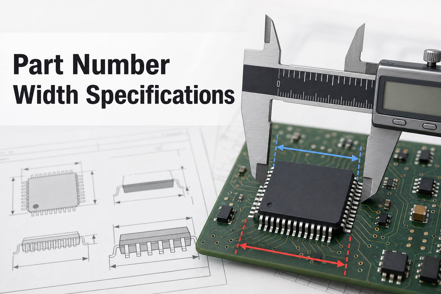
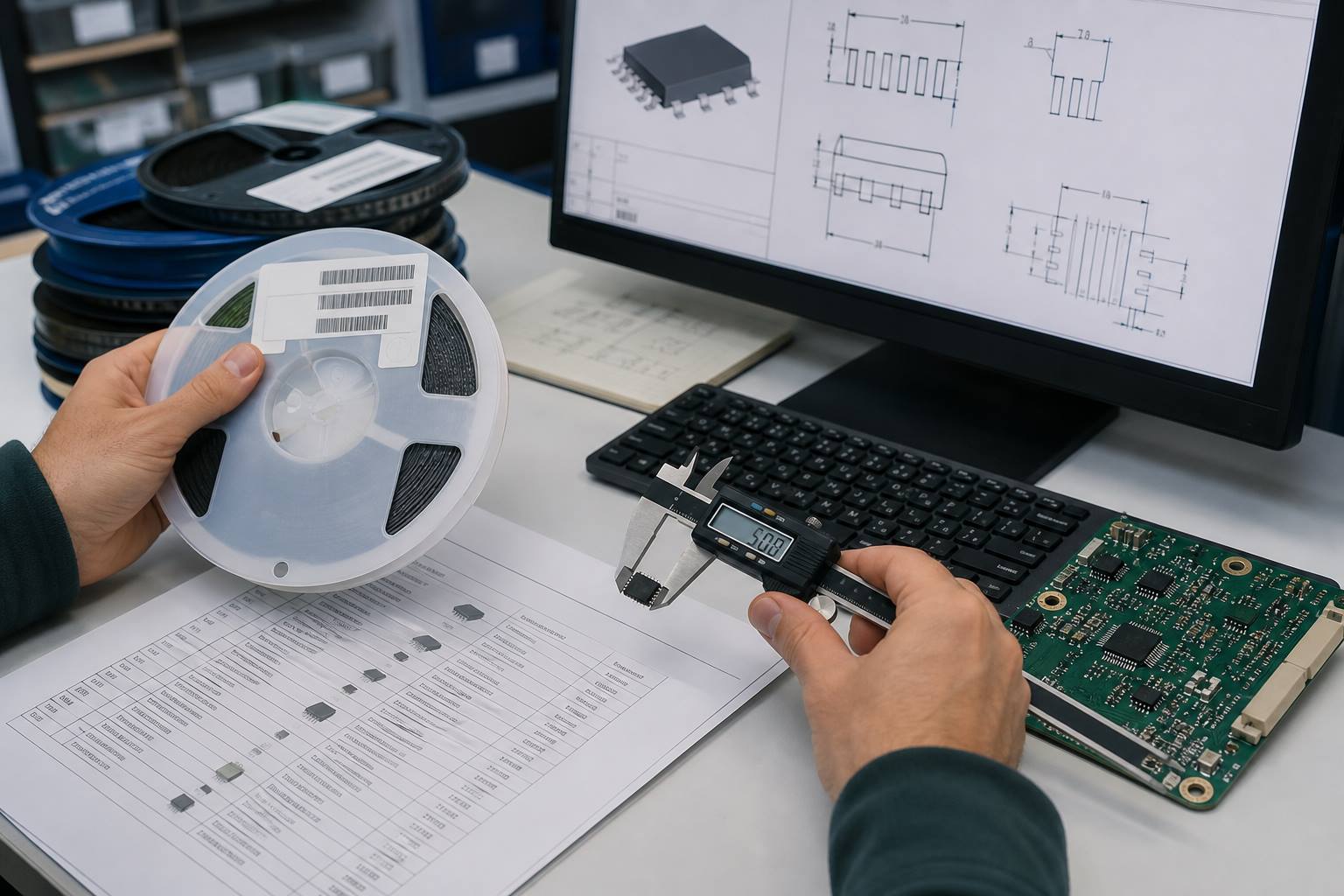
Digital caliper measuring an integrated circuit while a package drawing shows part number width specifications
Width verification starts with the exact manufacturer part number and its corresponding package outline drawing.

What Does Part Number Width Specification Mean?

A part number width specification is not one universal measurement; it is a set of mechanical dimensions associated with a specific orderable component. Depending on the package, ιˆ₯ζΈ¨idthιˆ₯?can refer to the molded body, the span across leads, the distance across terminals, an exposed thermal pad, or the tape-and-reel carrier.

This distinction matters because different teams use width differently. A mechanical engineer may need the maximum body envelope. A PCB designer needs terminal geometry and the recommended land pattern. A sourcing engineer must confirm that a proposed alternate uses a compatible package. A production engineer may also need carrier-tape width and component height for feeder setup.

Width term What it measures Why it matters
Body width Molded or ceramic package body, normally excluding leads Courtyard, enclosure clearance, neighboring-component spacing
Overall width or lead span Distance across the outermost leads or terminals Footprint fit, solder-joint geometry, inspection access
Terminal width Width of one lead, contact or termination Pad width, solder fillet and inspection criteria
Exposed-pad width Width of a thermal or ground pad under the package Stencil aperture, heat transfer, voiding and grounding
Land-pattern width Overall span of the recommended PCB pads Assembly yield and solder-joint reliability
Carrier-tape width Width of the tape used for automated placement Feeder selection and incoming material planning

Can You Read Width Directly from a Part Number?

Sometimes a part number contains a package or size code, but the code must be decoded with that manufacturer ordering guide. There is no universal rule that makes every suffix equal to a specific width.

For chip resistors and capacitors, codes such as 0402, 0603 and 0805 often describe a nominal length-by-width format. However, the same four digits can be interpreted in imperial or metric notation. An imperial 0603 is approximately 1.6 * 0.8 mm, while a metric 0603 is approximately 0.6 * 0.3 mm. The manufacturer, product family and datasheet determine which system applies.

For ICs, suffixes may indicate package family, pin count, temperature grade, packing method, lead finish or qualification option. Two electrically similar parts can have different widths because one uses SOIC, TSSOP, QFN or another package. Never remove the suffix during BOM cleanup unless the approved manufacturer documentation proves it is nonessential.

Where Are Width Dimensions Found in a Datasheet?

Width dimensions are normally located in the mechanical package drawing, package outline, dimensions section, or a separate package-document link referenced by the datasheet. The ordering-information table connects the exact MPN to the correct package name or drawing code.

  1. Search the exact MPN on the component manufacturer official website.
  2. Confirm the device family, revision and orderable status.
  3. Find the ordering guide and match the full suffix to the package option.
  4. Open the corresponding package outline drawing.
  5. Check the drawing units, dimension symbols, notes and tolerances.
  6. Use the recommended land pattern when one is provided; do not copy the body outline as the copper-pad outline.

Dimension letters vary by drawing system and package family. For example, a drawing may use one symbol for body width and another for overall width. Read the legend on that exact drawing instead of assuming that a familiar letter always means the same feature.

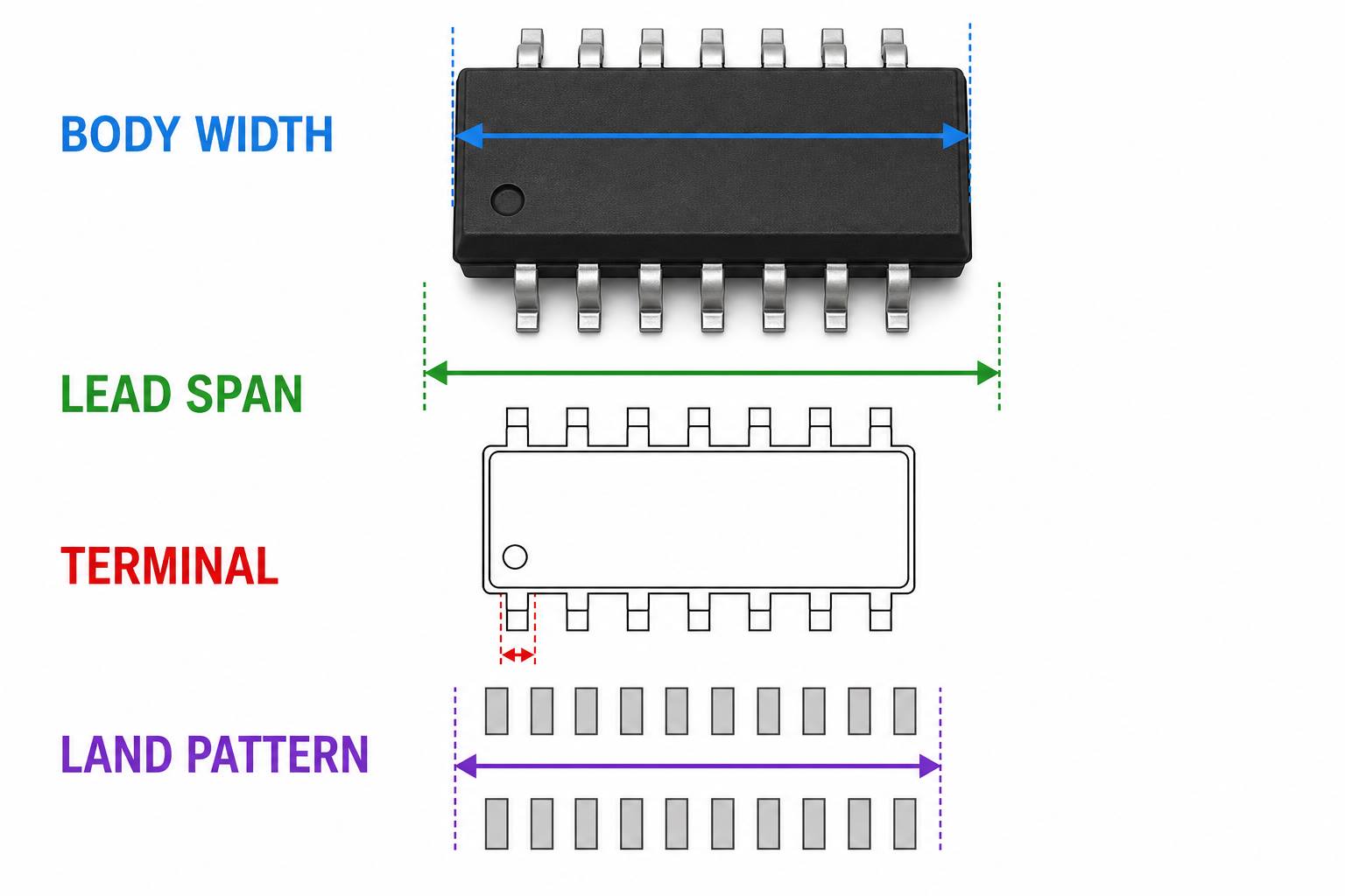
Body Width vs Overall Width vs PCB Land Pattern

Body width describes the component housing, overall width includes leads or terminals, and the PCB land pattern describes the copper pads needed to solder the component. These values are related but are not interchangeable.

Technical diagram comparing IC body width, lead span, terminal width and PCB land pattern width
The component body, lead span, individual terminal and PCB land pattern use different width references.

A common footprint error occurs when a designer treats the maximum package body width as the pad span. Gull-wing leads extend beyond the body and require toe, heel and side solder allowances. Leadless packages such as QFN use a different geometry, often including a central exposed pad and tightly controlled perimeter terminals. Connectors may add locating pegs, shell tabs, board-edge offsets or mating-envelope requirements beyond the visible contact width.

Use the manufacturer recommended footprint as the starting point, then review it against the PCB assembly process, solder paste, inspection method, density, rework access and the applicable company or industry land-pattern policy.

How to Interpret Minimum, Nominal and Maximum Width

Minimum and maximum values define the allowed manufacturing envelope; the nominal value is a reference target and may not represent every delivered part. PCB clearance and mechanical fit should normally account for the maximum component envelope, while solder-joint design must consider the complete terminal tolerance range.

Datasheets express tolerances in several ways: explicit minimum and maximum columns, a nominal value with plus/minus tolerance, or a basic dimension controlled by drawing notes. Units may be millimeters, inches, or both. Do not convert a rounded catalog value into a manufacturing limit. Use the dimension table attached to the package drawing and keep enough decimal precision to avoid changing the tolerance.

  • Use maximum body and lead span for keep-out and enclosure checks.
  • Use terminal minimum and maximum dimensions for pad and solder-joint review.
  • Use maximum height for enclosure, shielding and pick-and-place clearance.
  • Use the recommended footprint dimensions for PCB pads, not a visual estimate.
  • Check whether dimensions exclude mold flash, plating, burrs or terminal deformation.

How Common Package Codes Relate to Width

Package codes are useful search clues, but only the exact package drawing establishes the controlling width. Similar package names can cover different body widths, pitches, terminal styles and pin counts.

Package or code Width clue Required confirmation
0402, 0603, 0805 passives Often nominal length * width code Imperial vs metric system, tolerance, height and termination geometry
SOIC or SOP Narrow and wide body variants exist Body width, lead span, pitch, pin count and package drawing code
TSSOP, SSOP, MSOP Name suggests a small-outline family Exact pitch, body width, overall span and terminal dimensions
QFN or DFN Often described by nominal body length * width Terminal layout, exposed pad, wettable flanks and recommended land pattern
BGA, LGA or CSP Body size and array size may both be stated Ball or land pitch, matrix, missing positions, package height and courtyard
SOT family Family code identifies an outline series Manufacturer drawing, terminal count, lead form and alternate outline variants
Connector series Part number may encode positions or pitch Housing width, mating envelope, pegs, shell tabs and board-edge location

How to Verify an Exact MPN Before PCB Layout or Assembly

The most reliable verification method is a three-way match between the BOM, the official manufacturer package drawing and the PCB library footprint. Distributor filters and third-party CAD models are useful references, but they should not replace the manufacturer source.

  1. Lock the identity: record the manufacturer name and full MPN, including suffixes.
  2. Confirm the orderable package: match the MPN to the package code in the ordering guide.
  3. Record controlling dimensions: body width, lead span, pitch, terminal width, height and exposed-pad dimensions.
  4. Compare the footprint: verify pad geometry, pin numbering, courtyard, assembly outline and polarity mark.
  5. Check the physical supply: compare reel or tray label, top marking and incoming sample against the approved BOM.
  6. Approve deviations: treat any package or width difference as an engineering change, not a purchasing convenience.
Engineer comparing a BOM part number, component reel, package drawing, caliper and PCB footprint
A three-way check between the BOM, manufacturer drawing and PCB footprint catches package mismatches before placement.

What Should a BOM Include Besides the Part Number?

A production BOM should include enough information to distinguish the approved component and package without relying on a shortened description. At minimum, use the manufacturer, full MPN, value or function, package or footprint, quantity and reference designators.

Useful additional fields include tolerance, voltage or current rating, dielectric or material, temperature grade, lifecycle status, approved alternates, do-not-fit status and sourcing notes. BestPCBs provides a broader guide on how to make a PCB BOM, while the PCB component identification guide explains how markings, package shape and documentation work together.

BOM field Purpose
Manufacturer and full MPN Identifies the exact orderable device
Package or approved footprint Connects the component to PCB land geometry
Value, function and ratings Confirms electrical suitability
Reference designators and quantity Controls placement locations and purchasing quantity
Approved alternates Defines substitutions already reviewed by engineering
Revision and source document Maintains traceability when drawings change

What Problems Come from Using the Wrong Width?

An incorrect width can cause more than a cosmetic mismatch: it can make placement impossible, reduce solder-joint quality, create shorts, block inspection or interfere with nearby parts and the product enclosure.

  • Wrong pad span: leads do not sit correctly on the copper pads.
  • Insufficient solder fillet: pads are too short or narrow for the terminal tolerance.
  • Bridging risk: pads or stencil apertures do not match the actual pitch and lead width.
  • Courtyard collision: the maximum component body overlaps another device, shield or connector.
  • Assembly delay: incoming material fails the first-article check and must be replaced or the footprint redesigned.

  • Uncontrolled substitution: an alternate fits electrically but uses a different package outline.

If a mismatch is found before production, stop purchasing or placement, identify the controlling drawing revision, compare all affected dimensions, and obtain engineering approval. For unknown parts already on a board, start with the methods in the PCB components identification article rather than relying on one short top mark.

How to Evaluate Alternate Parts with Different Width Specifications

An alternate part is acceptable only when electrical, mechanical, thermal, regulatory and lifecycle requirements have been reviewed together.

Compare the full package drawing, not just the nominal body size. Check pin count and assignment, pitch, terminal style, coplanarity, exposed pad, package height, polarity orientation and the recommended land pattern. Then review the assembly process: paste aperture, reflow profile, AOI or X-ray access, feeder packaging and rework method. The alternate should be added to the approved BOM only after the responsible engineer accepts the comparison.

For projects that need purchasing and package verification support, BestPCBs explains its workflow on the component sourcing page and lists the usual production documents in its PCB assembly FAQ.

Part Number and Package Width Verification Checklist

Use this checklist before footprint release, BOM approval, alternate-part approval and first article assembly.

  • Manufacturer name and complete MPN are recorded.
  • Ordering suffix matches the intended package and packing method.
  • Datasheet and package drawing come from the official manufacturer source.
  • Drawing revision and units are confirmed.
  • Body width and overall terminal span are not confused.
  • Minimum, nominal and maximum dimensions are interpreted correctly.
  • Pin pitch, terminal width, package height and exposed pad are checked.
  • PCB pads follow an approved land pattern, not the body outline.
  • Courtyard, enclosure and rework clearances use the maximum envelope.
  • Alternate parts receive documented engineering approval.
  • Incoming reel, tray or tube label matches the approved BOM.
  • First article inspection confirms orientation and solder-joint geometry.

Frequently Asked Questions

Does the last number in a part number always indicate width?

No. Part-number structures are manufacturer-specific. A final digit or suffix may represent package, tolerance, temperature grade, packing, lead finish or another option. Decode it with the official ordering guide for that product family.

Is component width the same as footprint width?

No. Component width may describe the body or lead span, while footprint width describes the PCB land geometry. Pads usually extend or shift beyond terminal edges to create suitable solder fillets.

Which value should I use when a drawing lists minimum and maximum width?

Use the maximum package envelope for mechanical clearance. For footprint design, evaluate the complete range of terminal and package tolerances or use the manufacturer recommended land pattern.

Why do two distributors show different dimensions for the same MPN?

One listing may use nominal body size while another uses maximum size, overall lead span or rounded catalog data. Resolve the conflict with the current manufacturer datasheet and package drawing.

Are 0603 imperial and 0603 metric components the same size?

No. Imperial 0603 is about 1.6 * 0.8 mm, while metric 0603 is about 0.6 * 0.3 mm. Confirm the notation used by the manufacturer and CAD library.

Can I measure a component with calipers instead of reading the datasheet?

A physical measurement can support incoming inspection, but it cannot replace the drawing. One sample does not define the allowed tolerance, terminal geometry, coplanarity or recommended PCB land pattern.

Does the package name guarantee the same width across manufacturers?

No. Package family names may include multiple outlines, body widths and terminal configurations. Match the exact manufacturer package code and drawing before approving a cross.

What width matters for pick-and-place programming?

Placement setup can require component body dimensions, height, centroid and rotation, while feeder setup also depends on tape width and pocket geometry. Confirm the machine library against the supplied packaging.

Should the BOM contain package dimensions?

The BOM should at least contain the exact MPN and approved package or footprint. Critical dimensions may also be controlled in the library, assembly drawing or approved-parts record for traceability.

What should I send for a PCBA package-fit review?

Send Gerber or native PCB data, the complete BOM, pick-and-place file, assembly drawing, manufacturer datasheets for unusual parts, approved alternates, quantity and test requirements.

Final Takeaway

Part number width specifications must be read as part of a controlled identification chain: exact MPN, ordering code, package drawing, tolerance, PCB land pattern and incoming component. Do not assume that a package name, shortened part number or distributor filter proves mechanical compatibility.

If you are sourcing reliable PCB/PCBA manufacturing, including OEM, ODM, prototyping, mass production or custom engineering solutions, send your BOM, PCB files and package questions to the BestPCBs engineering team for technical support and a quote at sales@bestpcbs.com.

You may also like

Unlock the Secrets of Footprint PCB for Fast Turn PCB Fabrication
Tuesday, November 11th, 2025

A footprint PCB, PCB footprint, or land pattern, defines the precise arrangement of copper pads, solder mask openings, and sometimes silkscreen outlines on a printed circuit board where a component will be mounted and soldered. It is the critical physical interface between your schematic symbol and the real-world component, directly impacting solderability, reliability, and performance. This comprehensive guide will delve into the essentials of PCB footprint design, its pivotal role in avoiding manufacturing delays, and best practices for achieving successful, fast-turn PCB fabrication.

Have you ever faced frustrating delays, unexpected costs, or outright failure in your PCB board projects due to seemingly minor design errors? These issues often stem from a fundamental yet overlooked aspect: the PCB footprint. Common pain points include:

  • ​Solder Bridges and Open Connections:​​ Incorrect pad sizing or spacing leads to short circuits or poor solder joints.
  • ​Component Misalignment:​​ Inaccurate courtyard or silkscreen outlines cause parts to be misplaced during assembly.
  • ​DFM (Design for Manufacturing) Errors:​​ Footprints not optimized for your manufacturer’s processes result in fabrication issues.
  • ​Inconsistent Library Management:​​ Using outdated or unverified footprints from various sources introduces risk.
  • ​Prototype Re-spins:​​ A single footprint error can force a complete board revision, wasting time and money.

Fortunately, these challenges are entirely preventable with a disciplined approach. The solution lies in:

  • ​Adhering to IPC Standards:​​ Utilizing industry-standard guidelines for pad geometry.
  • ​Implementing a Centralized Library:​​ Maintaining a single, verified source for all PCB footprints.
  • ​Conducting Thorough DFM Checks:​​ Collaborating with your fabricator to validate designs.
  • ​Using Advanced Design Tools:​​ Leveraging software features for automated footprint generation and validation.
  • ​Partnering with an Experienced Manufacturer:​​ Choosing a fabricator like BEST Technology with expertise in high-precision footprint PCB production.

At BEST Technology, we specialize in fast-turn, high-precision PCB fabrication and assembly. Our deep understanding of PCB footprint design intricacies allows us to provide expert DFM analysis, ensuring your designs are not only electrically sound but also manufacturable, reliable, and delivered on time. For your next quick turn circuit boards project, pls feel free to contact us at sales@bestpcbs.com.

Footprint PCB

What is a PCB Footprint?

In PCB design, a footprint is the physical representation of an electronic component on the board layout. Think of it as a “footprint” left by the component. It does not define the electrical function but rather the physical connection points and keep-out areas.

  1. ​Key Elements of a Footprint:​​
    • ​Pads:​​ These are the copper areas where the component’s leads or terminals are soldered. They can be for through-hole (pads with holes) or surface-mount technology (SMT).
    • ​Solder Mask Opening:​​ This is an opening in the solder mask layer that exposes the copper pad, allowing for soldering. The opening is typically slightly larger than the pad.
    • ​Silkscreen Outline:​​ This is a non-conductive drawing on the board that shows the approximate shape and orientation of the component, aiding in assembly and debugging.
    • ​Courtyard:​​ This is a keep-out area that defines the space required for the component itself, ensuring no other parts are placed too close.
    • ​Reference Designator:​​ The unique identifier (e.g., R1, C5, U3) that links the footprint to its schematic symbol.
  2. ​Importance of Accuracy:​​ An incorrect ​PCB footprint​ is a primary cause of manufacturing defects. A pad that is too small can lead to a weak solder joint; a pad that is too large can cause solder bridging. Accurate ​footprint design​ is the first step toward ​fast turn PCB fabrication.

What is the Carbon Footprint of a PCB?

While “PCB footprint” primarily refers to the land pattern, the term “carbon footprint” relates to the environmental impact of manufacturing a PCB. This encompasses the total greenhouse gas emissions produced throughout the PCB’s lifecycle, from raw material extraction and processing to fabrication, assembly, shipping, and end-of-life disposal.

  1. ​Factors Influencing PCB Carbon Footprint:​​
    • ​Materials:​​ The energy intensity of producing copper foil, laminate substrates, and solder mask.
    • ​Manufacturing Processes:​​ Energy consumption from drilling, plating, etching, and lamination.
    • ​Transportation:​​ Emissions from shipping raw materials and finished boards globally.
    • ​Waste Management:​​ The environmental cost of treating and disposing of chemical waste and scrap boards.
  2. ​Reducing the Impact:​​ While the primary focus of this article is on the land pattern, choosing a manufacturer committed to sustainable practices, such as efficient energy use and waste reduction, can help minimize the overall ​PCB carbon footprint.

Why PCB Footprint Design Guidelines Matter in PCB Design Projects?

Following strict ​PCB footprint design guidelines​ is non-negotiable for the success of any ​PCB design project. These guidelines ensure that your design is manufacturable, reliable, and compatible with automated assembly equipment, which is crucial for ​quick turn PCB boards.

  • ​Ensuring Solderability and Reliability:​​ Guidelines provide rules for pad sizes, shapes, and spacing that promote proper solder fillet formation, preventing defects.
  • ​Facilitating Automated Assembly:​​ Precise footprints allow pick-and-place machines to accurately position components, increasing assembly speed and yield for ​fast turn printed circuit board assembly.
  • ​Preventing Signal Integrity Issues:​​ For ​high-speed PCB design, proper pad and via design within the footprint is critical to minimize parasitic effects and ensure signal quality.
  • ​Standardizing Design:​​ Guidelines create consistency across different designers and projects, reducing errors and streamlining the design process for ​rapid prototyping circuit boards.

How to Follow IPC Standards for PCB Footprints?

The IPC provides a set of industry-accepted standards that form the foundation of professional ​PCB footprint creation. Adhering to ​IPC standards for PCB footprints​ is the most effective way to guarantee compatibility and quality.

  1. ​Key IPC Standards:​​
    • ​IPC-7351:​​ This is the most important standard for ​PCB footprint​ generation. It provides mathematical models for calculating land pattern geometries based on component dimensions. It defines three density levels (Least, Nominal, Most) to balance solderability and space.
    • ​IPC-SM-782:​​ This older standard has been largely superseded by IPC-7351 but is still referenced.
  2. ​Using a PCB Footprint Calculator:​​ Many ECAD tools and online calculators are built around the IPC-7351 formulas. You input the component’s dimensions from its datasheet, and the calculator generates the compliant pad layout for your ​0805 PCB footprint, ​0603 PCB footprint, or complex components like a ​QFN footprint.
  3. ​Creating a Checklist:​​ Develop a ​PCB footprint checklist​ based on IPC standards to verify each footprint before releasing it to your library. This should include checks for pad size, solder mask expansion, and courtyard clearance.

How to Make a Component Footprint in PCB Layout Design?

Creating an accurate footprint PCB is a fundamental skill for any PCB designer. While the process can vary slightly between ECAD tools like Altium Designer, OrCAD, or KiCad, the core principles remain the same. Mastering footprint in PCB design ensures components fit correctly and solder reliably, which is essential for fast turn PCB fabrication.

Gather Component Data: Start with the manufacturer’s datasheet, which contains the critical dimensions needed for PCB footprint creation, such as pin spacing (pitch), pin width and length, and overall package dimensions. This step is crucial for building a PCB component footprint that meets design specifications.

Use ECAD Tool Features:

  • Manual Creation: Draw pads and outlines based on datasheet measurements. This method is suitable for custom or unusual components like a potentiometer PCB footprint or LED PCB footprint.
  • Component Wizard: Most professional tools have wizards to automate standard packages (resistors, capacitors, SOIC, QFP) creation by prompting for key dimensions. Common examples include 0603 PCB footprint or 0805 PCB footprint.
  • IPC-Compliant Footprint Generator: Advanced tools like Altium integrate generators using IPC standards for PCB footprints, creating highly accurate footprints that comply with pcb footprint design guidelines.

Verify the Footprint: After creation, cross-check it against the datasheet. Print at 1:1 scale and place the actual component (e.g., cherry mx PCB footprint, Arduino Nano PCB footprint) to confirm fit. This verification is invaluable for quick turn PCB boards and rapid prototyping circuit boards.

Key Takeaway: This section emphasizes footprint principles, dimensioning, and IPC standards, laying the foundation for reliable PCB designs in PCB board projects.

How to Build a Footprint for PCB​?

Building a PCB footprint transforms design principles into a practical layout that integrates seamlessly with manufacturing processes. It directly impacts the success of fast turn PCB fabrication, ensuring components fit correctly, solder reliably, and meet PCB footprint standards. A footprint, or land pattern, defines solder pads, silkscreen outlines, and keep-out areas.

1. Setting Up the PCB Library Environment

Create a dedicated PCB footprint library in ECAD tools like Altium Designer. This organizes all footprints for pcb design projects and accelerates fast turn custom PCB production.

  • Steps: File β†’ New β†’ PCB Library β†’ save with a descriptive name (e.g., β€œcypcblib1.pcblib”).
    A well-structured library is key to maintaining consistency in quick turn PCB fabrication workflows.

2. Creating the Footprint Using a Component Wizard

For standard components, wizards simplify footprint creation and ensure adherence to IPC standards for PCB footprints.

Steps:

  • Select Package Type: For example, SOP for surface-mount ICs or QFN footprint PCB layout for compact ICs.
  • Set Pad Dimensions: Define solder pad sizes from datasheets (e.g., length and width for SOP28).
  • Configure Spacing and Outline: Input pad pitch and overall dimensions; set silkscreen line width for clear component outlines.
  • Finalize and Name: Assign a unique name following pcb footprint naming convention for easy identification.

This workflow suits 0603 PCB footprint, 0805 PCB footprint, and standard surface-mount packages, reducing errors in fast turn prototype PCB boards.

3. Manual Footprint Design for Custom Components

For unconventional parts:

  • Pad Placement: Position pads accurately; specify hole sizes for through-hole components like through hole resistor PCB footprint or screw terminal PCB footprint.
  • Silkscreen and Keep-Outs: Draw outlines and define keep-out areas to prevent interference.
  • Validation: Cross-check against datasheets for reliable soldering and DFM analysis in quick turn PCB assembly.

4. Integrating Footprints into a Unified Library

Link footprints with PCB symbols to create a complete library:

  • Associate Footprints and Symbols: Ensure pcb footprint Altium integration maintains consistency across PCB library and PCB board projects.
  • Verify Integration: Confirm that updates propagate correctly using commands like altium update footprint from library.

Key Takeaway: This section focuses on practical footprint creation, library management, and tool-based integration, enabling efficient fast turn printed circuit boards production while adhering to PCB footprint design guidelines.

How Does a PCB Footprint Library Improve Fast Turn PCB Fabrication?

A well-managed, centralized ​PCB footprint library​ is a strategic asset that dramatically accelerates the PCB development cycle and enhances quality, directly enabling ​fast turn PCB fabrication.

  • ​Eliminates Redundant Work:​​ Engineers don’t waste time recreating the same ​PCB symbols​ and footprints for every new project.
  • ​Ensures Consistency and Accuracy:​​ A verified library containing all your ​PCB footprints​ (from ​capacitor PCB footprints​ to ​ESP32 PCB footprints) prevents the use of incorrect or outdated land patterns.
  • ​Streamlines DFM Analysis:​​ When a manufacturer receives a design with standardized, IPC-compliant footprints, their ​DFM analysis​ is faster and more straightforward, reducing the back-and-forth and speeding up production.
  • ​Facilitates Team Collaboration:​​ A shared library ensures all team members are working from the same source of truth, reducing errors in complex ​pcb board projects.

How to Read a PCB Footprint?

Reading a footprint is essential for debugging and verifying a PCB layout. You need to understand what each element represents.

  • ​Identify the Pad Types:​​ Distinguish between SMD pads (flat copper on the surface) and through-hole pads (with a drill hole in the center).
  • ​Check the Layers:​​ View the footprint in your ECAD tool across different layers (Top Layer for pads, Top Solder Mask for openings, Top Overlay for silkscreen). Ensure the solder mask opening correctly exposes the pad.
  • ​Understand the Courtyard:​​ This layer defines the physical boundary of the component. No other parts should encroach on this space.
  • ​Verify the Reference Designator:​​ Confirm it matches the schematic symbol.

Why Choose BEST Technology for High-Precision Footprint PCB Production and Assembly?

When your ​PCB design projects​ demand high precision and quick turnaround, the choice of manufacturer is critical. BEST Technology is the ideal partner for ​high-speed PCB​ and high-reliability applications.

  • ​Expertise in DFM:​​ We perform thorough ​PCB DFM​ checks, focusing on ​footprint PCB​ accuracy to catch potential issues before they reach production, saving you time and cost.
  • ​Advanced Manufacturing Capabilities:​​ Our facilities are equipped to handle the tight tolerances required for modern components, including micro BGAs and fine-pitch devices.
  • ​Commitment to Fast-Turn Services:​​ We understand the market’s need for speed. Our processes are optimized for ​quick turn PCB fabrication​ and ​quick turn PCB assembly​ without compromising on quality.
  • ​Technical Support:​​ Our engineering team can provide guidance on ​PCB footprint design guidelines​ and help optimize your design for manufacturability.

​To sum up, a footprint PCB is the foundational element that bridges electronic design and physical reality, determining the manufacturability, reliability, and success of a circuit board. Mastering its design and management is the key to unlocking efficient and fast-turn PCB fabrication. By understanding its components, adhering to IPC standards, and maintaining a rigorous library, you can avoid common pitfalls and accelerate your time to market. For manufacturers who prioritize precision and speed, partnering with a specialist like BEST Technology ensures that your intricate footprint designs are executed flawlessly. For your next high-precision PCB board projects, pls feel free to reach out to our team at sales@bestpcbs.com.

You may also like