PCB manufacturing PCB manufacturing
Home > Blog

PCB manufacturing files

How to Export Gerber Files from KiCad for PCB Manufacturing?
Tuesday, September 22nd, 2026

Here is how to export Gerber files from KiCad for manufacturing: create one Gerber file for each required PCB layer and separate drill files for holes and slots. Most fabricators expect both sets in one ZIP. Gerbers without drill data omit the hole pattern, while a native KiCad board file leaves the final plot choices to someone else.

The instructions match KiCad 10 and follow the files from the saved board through GerbView and into a revision-controlled ZIP. Older releases may label the menu differently, although File > Plot opens the plotting dialog in many earlier versions.

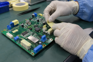
How to export Gerber files from KiCad, PCB design layers and fabrication output on an engineering workstation

What Should You Check Before Exporting Gerber Files from KiCad?

Check the KiCad source design before creating manufacturing files. The plotter reproduces the board as it exists; it does not repair an open outline, an unconnected net, an omitted layer, or an outdated copper-zone fill. Open the final production revision in PCB Editor and save it before running the checks.

  • Run the Design Rules Checker: Use Inspect > Design Rules Checker and review violations, unconnected items, and schematic-to-PCB differences. Resolve real problems and document any deliberate exclusions instead of assuming the fabricator will interpret them.
  • Validate Edge.Cuts: Confirm that the external outline is one closed, non-self-intersecting shape and that intended internal cutouts are also closed. KiCad shades a valid closed board area and reports malformed outlines through DRC.
  • Confirm the copper stack: Verify the enabled copper-layer count and order in Board Setup. A 4-layer board must have the correct internal layers and stack sequence before those layers are plotted.
  • Review mask and silkscreen: Check mask openings around pads and make sure silkscreen text and graphics do not cover exposed solderable areas. Remove information that does not belong on the manufactured board.
  • Inspect drilled features: Review plated through holes, non-plated holes, slots, and mounting holes. Confirm that each feature has the intended plating property and finished purpose.
  • Refill copper zones: Press B or use the zone-fill command, then save the board. Enabling KiCad’s plot-time zone check provides another safeguard, but the source board should already be current.

This preflight checks the editable design. It does not replace the later Gerber review, which checks the actual files that will leave your computer.

How to Export Gerber Files from KiCad Step by Step?

Use PCB Editor to export Gerber files from KiCad into a clean revision folder, then inspect what KiCad actually wrote. Each step below keeps the output tied to the same saved board revision and ends with something you can check.
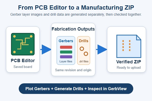
How to export Gerber files from KiCad, process from PCB Editor through separate Gerber and drill output to a verified ZIP
  1. Open the final board in PCB Editor: Confirm the project name and revision, save the .kicad_pcb file, and make sure the canvas shows the board you intend to order.
  2. Open the Gerber dialog: Choose File > Fabrication Outputs > Gerbers (.gbr). File > Plot opens the same dialog when Gerber is selected as the plot format. The Plot window should show the board’s enabled layer list.
  3. Choose a dedicated output folder: Use a new folder such as fabrication/rev-b/gerber. It should not contain files from an earlier revision. The output path displayed in the dialog should point to that folder.
  4. Select the required layers: Include every copper layer used by the design, the top and bottom solder-mask layers, any silkscreen layers that contain board markings, and Edge.Cuts. Add paste layers only when the package also serves a stencil or assembly workflow.
  5. Set the relevant plot options: Keep the drawing sheet out of the Gerbers, keep the plot at its real scale, use a consistent origin, and enable the zone-fill check. Change compatibility options only when your manufacturer provides a requirement.
  6. Click Plot: KiCad writes one Gerber file for each selected layer. Review the Output Messages panel and open the destination folder. You should see a fresh set whose timestamps match this export.

Do not ZIP the folder yet. First confirm the layer set, generate the drill output, and inspect both together.

Which Gerber Layers Should You Export for PCB Manufacturing?

A bare PCB package normally includes every used copper layer, both solder-mask layers, the required silkscreen layers, and Edge.Cuts. The exact count changes with the board stack and whether artwork exists on the back. The table separates bare-board files from stencil or assembly outputs.

Layer Purpose and Export Rule
F.Cu Front copper image; always export it when the board uses front copper.
B.Cu Back copper image; always export it for a 2-layer or multilayer board.
In1.Cu, In2.Cu, and other internal copper Inner signal or plane layers; export every enabled internal layer in the correct stack order.
F.Mask Front solder-mask openings; normally required.
B.Mask Back solder-mask openings; normally required.
F.Silkscreen Front legend and reference markings; export when used.
B.Silkscreen Back legend and reference markings; export when used.
Edge.Cuts External profile and internal cutouts; required for the manufactured board shape.
F.Paste and B.Paste Solder-paste stencil apertures; use for stencil or assembly preparation, not normally for bare-board fabrication.
F.Fab and B.Fab Assembly and fabrication drawing detail; send separately when requested and never substitute it for copper or Edge.Cuts.

For a typical 2-layer bare board, the practical minimum is F.Cu, B.Cu, F.Mask, B.Mask, Edge.Cuts, the silkscreen layers that contain artwork, and the drill file or files. For a multilayer design, add every internal copper layer and provide the intended stackup separately so the manufacturer can map the layer order without guessing.

Which KiCad Gerber Plot Settings Matter for PCB Manufacturing?

Keep the defaults that preserve 1:1 geometry, then change only options that affect file interpretation or compatibility. KiCad exposes many plot controls because the same dialog can also create PDF, SVG, DXF, and other outputs. A Gerber handoff uses a smaller, more focused subset.

  • Plot drawing sheet: off: The page border and title block are document furniture, not the PCB profile. Edge.Cuts should carry the board shape.
  • Check zone fills before plotting: on: KiCad warns that plot output can be wrong when outdated zones are not checked and refilled.
  • Plot on all layers: normally empty: This feature overlays selected items onto every base layer. Use it only for a deliberate documentation requirement, not to place Edge.Cuts or silkscreen into every Gerber by habit.
  • Gerber X2: use when accepted: X2 adds file-function, net, and other attributes that can help CAM interpretation. Turn it off only when a manufacturer reports that its older CAM system cannot process X2.
  • Protel filename extensions: optional: This changes names such as .gbr to familiar extensions such as .GTL and .GBL; it does not change the board geometry. Follow the recipient’s naming preference.
  • Gerber job file: useful but not a replacement: A .gbrjob file can carry stackup, material, and finish metadata. Keep the ordinary layer files and fabrication notes because not every CAM flow relies on the job file.
  • Coordinate format: manufacturer-bound: Use the fabricator’s recommendation when one is published. Do not change precision merely because an older tutorial shows a different KiCad release.
  • Origin: keep it consistent: Absolute origin is a common default when the manufacturer does not specify otherwise. If you use a drill/place origin, apply the same origin to the Gerber and drill outputs.

The current option definitions and compatibility notes are documented in the KiCad 10 PCB Editor manual. A manufacturer’s written CAM requirement takes precedence over a generic screenshot.

How Do You Generate Drill Files in KiCad?

Generate the drill data separately after plotting the Gerber layers. From the Plot dialog, click Generate Drill Files, or use File > Fabrication Outputs > Drill Files (.drl). Point the drill dialog to the same revision-specific output folder and keep its origin consistent with the Gerbers.

  • Choose Excellon for broad compatibility: KiCad states that most PCB manufacturers require Excellon. Use Gerber X2 drill output only when the recipient explicitly accepts it.
  • Leave Mirror Y axis off: KiCad advises against mirroring when a third party manufactures the PCB.
  • Leave Minimal header off: Enable it only when the manufacturer asks for a reduced header.
  • Keep PTH and NPTH separate by default: KiCad normally writes plated and non-plated holes to separate Excellon files. Merge them only when the manufacturer requests a single drill file.
  • Keep alternate oval-hole mode off: The normal route-command representation suits most manufacturers. Use the alternate mode only for a stated CAM requirement.
  • Generate and inspect the output: Click Generate, confirm that the messages contain no unresolved errors, and verify that the expected .drl file or files appear with the new Gerbers.

A drill map can help a human review the hole pattern, but it does not replace the machine-readable drill file. If blind, buried, or laser-drilled vias are involved, also send the stackup and via-span requirements because a flat file list does not fully describe the fabrication sequence.

How Do You Verify KiCad Gerber and Drill Files Before Manufacturing?

Load the exported Gerber files and Excellon drill files together in GerbView and inspect the manufacturing data, not the original PCB canvas. KiCad’s Gerber Viewer lets you switch layers on and off, compare their alignment, and view drill data over the copper and outline.
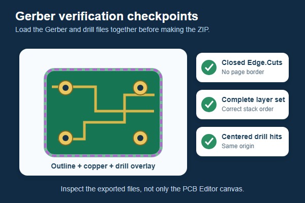
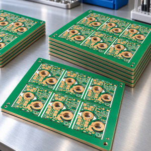
How to export Gerber files from KiCad, Gerber outline copper layers and drill hits checked together before manufacturing
  1. Load the complete export: Open all Gerber layers, then load every Excellon drill file. The correct result is one entry for every expected copper, mask, silkscreen, profile, and drill output, with no file from an older revision.
  2. Check the board outline: Edge.Cuts should show one continuous external profile plus only the intended internal cutouts. The displayed dimensions should match the source design, without a page border or unexpected outer rectangle.
  3. Inspect copper in stack order: Toggle each copper layer and check that its routing, pads, planes, and board position belong to that layer. A multilayer set should contain every intended copper layer once, in the expected order.
  4. Compare mask with pads: Solder-mask openings should align with exposed pads, test points, and other intended copper. Unexpected solid mask over a pad is a reason to return to the source board.
  5. Review silkscreen clearance: Text should remain readable, appear on the intended side, and stay off exposed pads. In the finished-board view, bottom-side text should have the expected orientation rather than looking accidentally mirrored.
  6. Overlay drill hits: Plated holes should sit inside their pads, while non-plated mounting holes and slots should align with the outline and mechanical features. A consistent offset across the board points to mismatched origins.
  7. Check high-risk details: Zoom into fine-pitch footprints, connector rows, mounting holes, slots, board-edge features, and dense via fields. The correct export should preserve the same clearances and feature positions you approved in the source board.

A successful Plot message proves that KiCad wrote files; it does not prove that you selected every required layer or that the output represents the intended revision. When anything looks wrong, repair the source board, delete the affected export set, regenerate Gerbers and drills together, and repeat the viewer inspection.

What Should a Complete KiCad PCB Manufacturing Package Include?

Gerber files describe layer images and board geometry, but they do not communicate every manufacturing requirement. A complete handoff combines the exact files you inspected with the construction details that a fabricator cannot safely infer from those images.

  • Verified Gerber set: Include the same complete layer set that you loaded and checked in GerbView, without files from another revision.
  • Machine-readable drill data: Include the Excellon PTH and NPTH output generated for that Gerber set. A drill map is useful for review but is not a production drill file.
  • Stackup and construction details: State the layer order, material, finished thickness, copper weight, and any blind, buried, laser-drilled, filled, or capped via requirements.
  • Fabrication notes: Specify surface finish, controlled impedance, critical tolerances, panelization, special routing, and other order-specific requirements.
  • Optional Gerber job file: Include the .gbrjob file when generated and accepted, but do not use it instead of the individual Gerber, drill, and fabrication files.

If the same project also includes assembly, the assembler may request a BOM, component placement file, assembly drawings, paste layers, programming data, and test instructions. Those are PCBA inputs and should not be confused with the bare-board Gerber and drill package.

How Should You Package and Send KiCad Gerber Files to a Manufacturer?

Create the ZIP from the exact folder you inspected, then keep that verified archive unchanged for upload. This simple rule prevents a late file replacement from breaking the relationship between the viewer check and the package that reaches the manufacturer.

  1. Start from an empty revision folder: Remove or archive the previous output before plotting. Never mix a new copper layer with an old outline or drill file.
  2. Generate Gerbers and drills in one session: Matching timestamps are not a substitute for revision control, but they make accidental carryover easier to spot.
  3. Verify that exact set: Load the folder’s Gerbers and drills into GerbView. Do not inspect one folder and ZIP another.
  4. Use a clear archive name: Include the project and revision, such as controller-rev-b-fab.zip, without spaces or ambiguous words such as final-final.
  5. Attach the fabrication notes: State quantity, material, stackup, finished thickness, copper weight, surface finish, impedance requirements, tolerances, delivery location, and any special process requirement that is not unambiguously encoded in the image files.
  6. Review the manufacturer’s preview: If the upload portal renders the ZIP, compare the outline, layer count, dimensions, and drill pattern with your verified GerbView result before placing the order.

A .kicad_pcb file can be useful for engineering discussion, but it is not a universal substitute for fabrication output. Send it only when the manufacturer accepts native KiCad data and you are comfortable sharing the editable design. Keep the approved Gerber and drill archive as the order’s controlled manufacturing package.

Which KiCad Gerber Export Mistakes Cause Manufacturing Problems?

The most consequential errors are missing outline or drill data, wrong layer selection, mixed revisions, and inconsistent origins. The first symptom usually points to a narrow check, so correct the source or export decision instead of changing unrelated settings.

Issue Impact and First Fix
Edge.Cuts missing or open The board outline cannot be interpreted correctly. Close the outline and re-export Edge.Cuts.
Drill files omitted Holes and vias are missing. Generate and include the Excellon drill files.
NPTH file omitted Mounting or tooling holes may be missing. Include the separate NPTH drill file.
Inner layer missing Multilayer connectivity may be incorrect. Check the stackup and re-export all copper layers.
Gerber and drill origins differ Drill hits are shifted from pads. Use the same origin for both outputs.
Mixed revisions Layers and holes may not align. Clear the output folder and export one revision.
Wrong extra layers included The manufacturing package becomes ambiguous. Remove unrelated paste or fabrication outputs.
Files not inspected Missing or shifted output may go unnoticed. Verify the exported files in GerbView.

Silkscreen over exposed pads is another frequent review finding, but it is not solved by selecting more files. Correct the source artwork or use the approved silkscreen-to-mask handling, then regenerate and inspect the affected silkscreen and mask layers.

FAQs About KiCad Gerber Export

Q1: Does the .gbrjob file include the drill data?

A1: No, the .gbrjob file does not include drill data. KiCad creates it as part of the Gerber export, while hole data is generated separately. Include the Excellon .drl files even when a .gbrjob file is present.

Q2: Can a drill map replace the .drl file?

A2: A drill map cannot replace the .drl file. It is a visual aid for reviewing hole locations and tool sizes. The manufacturer still needs the machine-readable drill file, normally in Excellon format.

Q3: How should slots and internal cutouts be included?

A3: Put board cutouts on Edge.Cuts and configure slots through their pad or drill properties. Use closed shapes for cutouts and set the correct plating property for each slot. Open the Gerbers and drill files together to confirm that every routed feature is present and aligned, and follow the manufacturer’s minimum slot and routing rules.

Q4: Why does the manufacturer’s preview show a full sheet or an oversized board?

A4: A page border or stray item is probably expanding the preview. Check that Plot drawing sheet is off, Edge.Cuts contains one valid closed outer profile, and Edge.Cuts was not added to every layer through Plot on all layers. The preview should show the board outline, not a full page or an unexpected rectangle.

Q5: Can KiCad open or edit the Gerber files after export?

A5: Use GerbView to inspect Gerbers, not as a substitute for the KiCad source design. GerbView can export limited geometry to PCB Editor, but that conversion does not recreate the original netlist, footprints, constraints, or full design intent. Make changes in the .kicad_pcb source, then export a new manufacturing set.

Q6: Do Gerber files include the BOM and component placement data?

A6: Gerber files do not include the BOM or component placement data. They describe the board’s fabricated layer images. Automated assembly normally requires a BOM and a component placement or centroid file in addition to the PCB manufacturing package.

Q7: Should I use different KiCad settings for JLCPCB or another manufacturer?

A7: Follow the manufacturer’s current requirements when they differ from KiCad’s general defaults. The essential checks stay the same: export every required layer, generate the drill files separately, keep the origins consistent, and inspect the exact upload package. A board-house profile does not replace GerbView inspection or the portal preview.

A reliable KiCad handoff comes from four controls: a checked source board, a complete layer and drill export, a viewer inspection of the actual files, and separate notes for requirements that images cannot fully express. That sequence is more dependable than copying a settings screenshot from a different KiCad release or manufacturer.

Once your KiCad Gerber and drill files have been verified, send the ZIP together with your stackup, material, copper weight, surface finish, impedance requirements, quantity, and delivery requirements to sales@bestpcbs.com. EBest Circuit can review the manufacturing package before PCB fabrication and provide a quotation based on the actual board requirements.


You may also like

What Is an ODB++ File? Structure, Export, and Review Guide
Tuesday, September 1st, 2026

An ODB++ file is a PCB manufacturing data package that combines layer artwork, drill data, board geometry, net information, component details, and other production data in one structured dataset. PCB designers export it from their design software and send it to a fabricator or assembler for CAM preparation.

Its main difference from a Gerber package is context. Gerber files normally describe individual layers, while ODB++ can also preserve how layers, holes, nets, and components relate to one another. This guide explains what is inside the package, how to export and view it, when to choose it over Gerber, and what to check before sending it for PCB manufacturing.

ODB++ file, PCB manufacturing data displayed on an engineering workstation

What Is an ODB++ File in PCB Manufacturing?

ODB++ is a PCB manufacturing data package that places the information for one board in a connected, machine-readable structure. The package can include copper and mask layers, board outlines, holes, routes, nets, parts, pins, and attributes. A CAM system can therefore read both the features and much of the meaning behind them.

ODB++Design is the branch of the ODB++ family used to pass PCB design data into manufacturing. Siemens maintains the format and provides specifications, sample jobs, and viewer resources through the official ODB++Design resource hub. When a PCB manufacturer imports the job, the software can identify layer types, drill relationships, connectivity, and component information without reconstructing all of that context from separate files.

The package only contains what the PCB design tool exports. If a layer, netlist, component field, or manufacturing note is missing at the source or disabled in the export settings, the ODB++ job will not add it automatically. Inspect the exported layers and compare the job with the source PCB so a missing selection does not reach CAM review.

Is an ODB++ File a Single File or a Folder Structure?

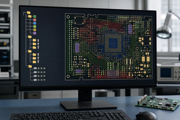
An ODB++ job is a folder structure, even when it arrives as one compressed file. Design tools commonly package the job as a .tgz, .tar, or .zip archive for easier transfer. After extraction, the archive contains a directory tree rather than one universal .odb file.

The tree separates different kinds of PCB data so that CAM software can find and connect them. Common sections include:

  • Matrix: acts like a map of the job. It identifies the layers, their order and type, and the relationship between drill spans and board layers. CAM software uses it to understand which files represent copper, solder mask, legend, drill data, and other functions.
  • Steps: contains the actual board, panel, coupon, or repeated layout. Each step can hold its profile, graphical features, holes, routes, nets, and component data.
  • Symbols: stores reusable shapes referenced by pads and other features. Reusing a symbol keeps the job organized instead of describing the same geometry repeatedly.
  • Fonts: provides character definitions used for text in the job.
  • Input and miscellaneous data: may contain source references, attributes, logs, user data, or other job-level information created by the exporter.
ODB++ file, CAM workstation showing a PCB data hierarchy and multilayer board

Altium’s CAM import and export documentation describes an ODB++ job as a directory tree of readable ASCII files. Send the original archive or the complete extracted tree. If only a few internal folders are copied, the receiving software may lose the matrix, step, or symbol references it needs to open the board correctly.

What Information Does an ODB++ File Contain?

An ODB++ file can contain most of the design data a manufacturer needs to interpret a PCB. Each data group supports a different CAM, fabrication, assembly, or inspection task:

  • Board profile and layer stack: defines the board boundary and identifies copper, solder mask, paste, legend, mechanical, and other layers. CAM uses this information to place every production layer in the correct sequence.
  • Copper and mask features: includes pads, tracks, planes, clearances, openings, and other plotted geometry. These features become the basis for imaging, solder mask, and paste preparation.
  • Drill and route data: describes hole sizes, plated or non-plated status, slots, and routed outlines. The fabricator uses it to prepare drilling and mechanical routing operations.
  • Electrical connectivity: connects features to named nets. This helps CAM engineers compare the manufactured geometry with the intended circuit and prepare electrical test data.
  • Components and packages: can include reference designators, locations, rotations, board sides, pins, and package relationships. Assembly teams can use this context when preparing placement and inspection data.
  • Attributes: adds meaning to layers, pads, holes, components, or other features. An attribute may identify a test point, via type, component pin, or special feature more clearly than geometry alone.
  • Board and panel steps: can represent a single PCB, production panel, coupon, or repeated placement. This allows the recipient to see how the job is organized rather than guessing from separate images.

The exact content varies by design tool and export settings. For example, Altium lets the user select plotted layers, archive type, ODB++ version, and netlist inclusion. A job exported without net data can still open normally, but the manufacturer cannot use it for the same connectivity comparisons as a job that includes the netlist.

How Is an ODB++ File Different from Gerber Files?

ODB++ combines PCB geometry and relationship data in one structured job, while a Gerber release is usually a set of artwork and supporting files. Both formats can support successful PCB fabrication. The better choice depends on the data your design tool can export and the format your manufacturer can process reliably.

Decision point ODB++ file Gerber package
Package model One directory tree or archive with linked job data Multiple artwork and supporting files
Layer meaning Layer type and order can be explicit in the matrix Depends on file functions, attributes, names, and supporting notes
Connectivity Can include nets and feature relationships Usually needs an IPC-D-356 or other independent netlist
Component context Can carry components, pins, packages, and placements Usually supplied through separate placement and assembly files
Review risk Wrong export options can omit expected job intelligence Missing, duplicated, or mismatched files can obscure relationships
Best choice Use when both the source CAD tool and recipient support ODB++ Use when the recipient requests Gerber or already has a tested Gerber workflow

Choose ODB++ when the manufacturer supports it and you want to send layer, net, component, drill, and attribute data together. It is especially useful for complex multilayer boards, dense layouts, and jobs that benefit from richer CAM checks.

Choose Gerber when the supplier requests it, the project uses a well-established Gerber workflow, or the handoff is limited to straightforward fabrication artwork and its supporting files. Gerber X2 can also carry useful attributes, so the comparison is not simply “smart” data versus “basic” data.

If you provide both formats, generate them from the same PCB revision and make one format the agreed manufacturing source. Two packages from different revisions create conflicting instructions rather than useful redundancy.

How Do You Create an ODB++ File from PCB Design Software?

Create an ODB++ file with the fabrication-output or manufacturing-export command in your PCB design software. Export directly from the native PCB design when possible because the source project contains the layer, net, component, and attribute relationships that a conversion from artwork may not recover.

  1. Open the finished PCB layout. Confirm that the outline, layer stack, holes, and design rules reflect the version you intend to send.
  2. Start the ODB++ export. Choose the fabrication-output or manufacturing-output command provided by the design tool.
  3. Review the settings. Select the correct board or panel, required layers, units, netlist option, archive type, and ODB++ version accepted by the recipient.
  4. Export to a new folder. Keeping the output separate from older jobs makes it easier to identify the current package.
  5. Open the result in a viewer. Check that the visible board, layers, holes, and nets match the source design.

In Altium Designer, current documentation places the command under File → Fabrication Outputs → ODB++ Files, and an Output Job can also generate it. In KiCad PCB Editor, use File → Fabrication Outputs → ODB++ Output File. In Fusion Electronics, use Export ODB++ from the Manufacturing toolbar.

Menus and available options can change between software versions. Check the current instructions for Altium ODB++ output, KiCad PCB Editor output, or Fusion Electronics export. Pay particular attention to the netlist, selected layers, units, panel or board step, archive format, and ODB++ version.

How Do You Open and View an ODB++ File?

Use an ODB++ viewer when you only need to inspect the package; use compatible CAM software when you need manufacturing analysis or process preparation. Open the complete archive or the root job folder. A suitable tool should display the board step, profile, layers, copper features, drills, nets, and any component data that the package contains.

  • Local viewing: Siemens offers an ODB++ Viewer for inspecting ODB++ models on a local system.
  • Browser viewing: the Altium 365 Viewer lists ODB++ among its supported formats and can be useful for a quick visual review.
  • CAM review: a fabricator or CAM engineer can import the job into manufacturing software to analyze layers, tools, nets, clearances, and production features.

For confidential designs, a local viewer avoids uploading the package to a third-party service. If you use an online viewer, review its current privacy, retention, access, and deletion terms first.

What Should You Check Before Sending an ODB++ File?

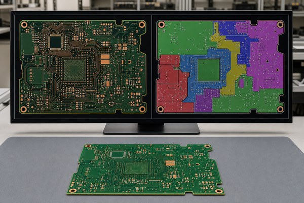
Before sending the package, open it in a separate viewer and compare six areas with the source PCB. The goal is to catch missing or incorrectly mapped data while the design files are still available.

  1. Board outline: confirm the outer profile, cutouts, slots, dimensions, and units. A missing or duplicated outline can change the routed board shape.
  2. Layers: compare the copper, solder mask, legend, paste, and mechanical layers with the PCB stack. Check both layer count and order.
  3. Drills and slots: review hole sizes, plated and non-plated holes, blind or buried drill pairs, backdrills, and routed slots where applicable.
  4. Nets: make sure net names and connectivity are visible if a netlist was included. Review critical planes, net ties, and intentional shorts rather than assuming they transferred correctly.
  5. Component data: when the job supports assembly, compare reference designators, board side, rotation, pin positions, and omitted or variant parts.
  6. Revision consistency: give the archive a clear part number and revision, and make sure its drawing, stackup, BOM, and placement files describe the same design version.
ODB++ file, comparison of source PCB design and CAM layer view

For more detail on how manufacturers use connectivity data, the PCB bare board testing guide explains how a board’s net data supports continuity and isolation testing.

What Information May Still Need a Separate Drawing or Note?

ODB++ contains extensive PCB manufacturing data, but it does not necessarily replace fabrication drawings, stackup requirements, BOMs, assembly drawings, or special process notes. These documents explain requirements that may not be included by the exporter or may need a clear written tolerance.

  • Fabrication details: material family, finished thickness, copper weight, surface finish, filled or capped vias, edge plating, and other special processes.
  • Stackup and impedance: dielectric construction, target impedance, tolerance, reference layers, coupon needs, and reporting requirements.
  • Mechanical requirements: critical dimensions and tolerances, bevels, countersinks, scoring, routing quality, and keep-out areas.
  • Panelization: array size, rails, fiducials, tooling holes, breakaway method, coupons, and any restrictions on how the manufacturer may panelize the board.
  • Assembly information: BOM, approved parts, placement data, assembly drawing, variants, polarity notes, programming, inspection, and functional test instructions.

This limitation often depends on the exporter rather than the format alone. Ansys, for example, documents cases in which an imported ODB++ directory lacks material or layer characteristics required for analysis and needs a separate control file. Ask the PCB manufacturer which supporting documents it expects instead of assuming the archive replaces every drawing and note.

Why Can an ODB++ File Fail to Import or Pass CAM Review?

Import failures usually come from incorrect packaging, missing export content, layer mapping errors, or a compatibility difference between tools. Start with the visible symptom, then check the corresponding source setting.

Problem Likely cause What to check
The viewer cannot find a job The archive has an extra wrapper folder or an incomplete directory tree Open the archive and confirm that the matrix and steps folders belong to the same job root
The board opens without layers or an outline Required layers or the board profile were not selected during export Review the layer-selection and outline settings, then export again from the native PCB
Drills or slots appear in the wrong place Units, drill pairs, plating types, or layer mapping do not match Compare tool sizes, units, plated status, and start and stop layers with the source design
Nets are missing The netlist option was disabled or the wrong board step was exported Enable net data, select the correct step, regenerate the package, and confirm that nets appear in the viewer
Stackup or materials are incomplete The exporter did not include the required attributes Check the exported data and provide a separate stackup or material note when needed
One tool opens the job but another rejects it The importer does not support the archive type, format version, or an exported feature Record both software versions and the first error; try the complete uncompressed job if archive support is uncertain

Regenerate the package after correcting the source or export settings. Manually deleting folders or editing coordinates may hide the original problem and create a package that no longer matches the PCB design.

How Should You Control Revisions and Protect ODB++ Data?

Use a clear file name that includes the PCB part number and revision. Keep the ODB++ package, fabrication drawing, stackup, BOM, placement data, and assembly drawing on the same revision. Before sending them, compare the part number and revision on every file. A mismatch can cause the manufacturer to build geometry from one version and assembly data from another.

After a design change, create a new export from the updated source project. Do not place the new drawing beside an old ODB++ package or reuse an old archive with a renamed file. If the manufacturer finds a CAM issue, update the source design where appropriate before generating the next package.

An ODB++ job can reveal copper geometry, connectivity, component positions, and other design details. Send confidential jobs through a transfer method that provides suitable access control, and avoid uploading them to an online viewer unless its data terms fit the project.

FAQs About ODB++ Files

Q1: What is the ODB++ file extension?

A1: The package has no single mandatory extension. It may be an uncompressed job directory or a .tgz, .tar, or .zip archive. Identify it by its job structure and a compatible viewer, not by a generic .odb suffix.

Q2: Is ODB++ free to view?

A2: A free official viewer is available. Siemens describes its ODB++ Viewer as a free solution. Access conditions, platform support, and resource registration can change, so check the current official download page before relying on a particular deployment.

Q3: Can you convert Gerber files to an ODB++ file?

A3: Conversion cannot recreate missing design intelligence. A CAM tool may import Gerber and drill data and export an ODB++ job, but it can only organize the information it received or inferred. It cannot reliably recover original nets, component relationships, stackup intent, or attributes that were never supplied.

Q4: Does an ODB++ file include a BOM and pick-and-place data?

A4: Do not assume it does. ODB++ can carry component and placement-related information, but exporters and assembly workflows differ. Send a matching BOM, placement file, assembly drawing, and variant instructions unless the assembler confirms that the job contains every required field.

Q5: Can a PCB manufacturer build from only an ODB++ file?

A5: Only when the package contains all required manufacturing information. Many jobs still need a fabrication drawing, stackup, material and finish notes, impedance requirements, tolerances, panel instructions, and order quantity.

Q6: Where can you find an ODB++ file example?

A6: Use the official sample. The ODB++Design resource hub provides a current sample package alongside specification resources, which is safer than treating an unknown archive as a format reference.

Q7: How do you open an ODB++ file?

A7: Open the complete archive or root job folder in a compatible viewer. Use a local ODB++ viewer for confidential data, a browser viewer for convenient visual review, or CAM software when manufacturing analysis is required.

Q8: Can Altium Designer, KiCad, and Fusion Electronics export ODB++?

A8: Current versions of all three tools provide ODB++ export options. The menu path and available settings vary by version, so confirm the selected layers, units, netlist, archive type, and ODB++ version before generating the package.

Q9: Why will an ODB++ file not open?

A9: Packaging and compatibility problems are common causes. Check for an extra wrapper folder, an incomplete job tree, an unsupported archive type, or a format version that the receiving viewer cannot import.

Q10: Should you send ODB++ and Gerber files together?

A10: Send both only when the manufacturer requests them. Generate both packages from the same PCB revision and identify which format controls manufacturing so the recipient does not have to resolve conflicting data.

How Do You Prepare a Reliable ODB++ Handoff?

ODB++ is most useful when you want to give a PCB manufacturer one structured package with geometry, layer, drill, net, and component context. Export it from the native PCB design, review the result in a separate viewer, and make sure the package opens with the correct outline, layers, holes, and connectivity.

Use the format when your manufacturer supports it and the additional data helps with CAM preparation or assembly. Keep separate drawings and notes for material, stackup, impedance, finish, tolerances, panelization, and assembly requirements that the package does not clearly contain. Above all, make sure every file belongs to the same PCB revision.

Before production, compare the ODB++ package with the source design and use a practical PCB design for manufacturability checklist to confirm the remaining build details. For a project-specific CAM and manufacturing review, send the ODB++ file and its matching documents to EBest Circuit at sales@bestpcbs.com.

You may also like