PCB manufacturing PCB manufacturing
Home > Blog

High Voltage PCB Design

High Voltage PCB Design Guidelines for Safe and Reliable Boards
Friday, August 28th, 2026

A high voltage PCB has to do more than carry a higher electrical potential. Its layout, insulation system, laminate, conductor geometry, surface condition, and manufacturing tolerances all influence whether the finished board can operate safely without arcing, surface tracking, insulation breakdown, or premature field failure.

EBest Circuit supports high-voltage PCB fabrication and PCBA projects from prototype through production. For projects involving special insulation spacing, heavy copper, controlled dielectric thickness, isolation slots, or unusual stack-ups, send your Gerber files, stack-up, operating voltage, peak voltage, material requirements, and application information to sales@bestpcbs.com for an engineering review and quotation.
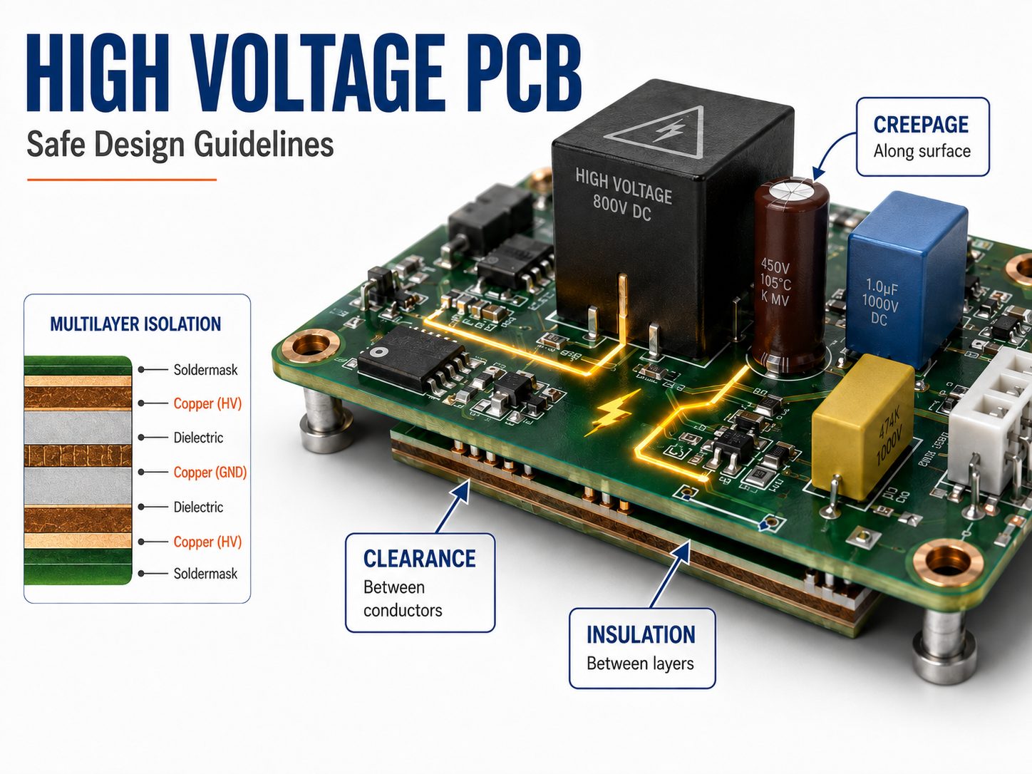
High voltage PCB design guidelines showing creepage, clearance, insulation, and multilayer isolation

What Is a High Voltage PCB?

A high voltage PCB is a circuit board designed with additional insulation, spacing, material, and layout controls to safely handle elevated voltage differences between conductors.

There is no single PCB-industry voltage threshold above which every circuit automatically becomes a high-voltage PCB. In practical power-electronics work, approximately 300 V to 1,000 V is a useful range where high-voltage spacing and insulation considerations become increasingly important, while properly engineered boards can operate above 1 kV.

Typical applications include:

  • EV charging and battery systems
  • Industrial power supplies
  • Solar inverters
  • Motor drives
  • High-voltage test equipment
  • Medical electronics
  • Power conversion equipment
  • Energy storage systems
  • High-voltage measurement circuits

The key distinction is therefore not simply the number printed beside the voltage rail. A reliable design has to manage insulation coordination across traces, pads, layers, component leads, PCB edges, slots, coatings, and the surrounding environment.

How Much Voltage Can a PCB Handle?

For practical high-voltage PCB design, working voltages around 300–1,000 V are common design territory, while specially engineered PCBs can operate above 1 kV; there is no universal maximum PCB voltage rating.

The actual limit is usually determined by the weakest insulation path rather than by the FR-4 laminate alone.

For example, a laminate may have high dielectric strength while an assembled PCB still fails because two exposed pads are too close, contamination forms a conductive surface path, or an unexpected surge exceeds the designed clearance.

Voltage capability is influenced by:

  • Working voltage: continuous or repetitive voltage between conductors
  • Peak voltage: maximum DC or AC peak potential difference
  • Transient voltage: switching spikes and surge events
  • Clearance: shortest air path between conductive parts
  • Creepage: shortest surface path between conductive parts
  • Dielectric thickness: insulation between PCB layers
  • Material CTI: resistance to surface tracking
  • Altitude: lower air pressure reduces air insulation capability
  • Pollution and moisture: contamination can reduce surface resistance

For design and RFQ purposes, it is therefore more useful to specify working voltage + peak/transient voltage than to state only “1,000 V PCB.”

What Is the Difference Between Creepage and Clearance in High Voltage PCB Design?

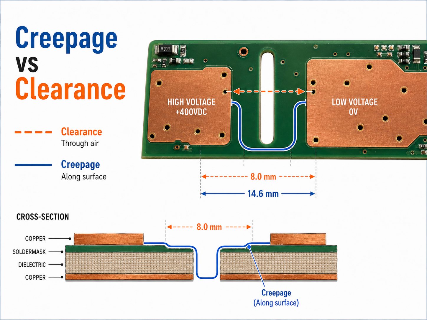
Clearance is the shortest distance through air between two conductive parts, while creepage is the shortest distance along an insulating surface.

Parameter What It Measures Main Failure Risk
Clearance Shortest path through air Arcing / air breakdown
Creepage Shortest path along an insulating surface Surface tracking
Solid insulation Path through dielectric material Dielectric breakdown
Creepage versus clearance on a high voltage PCB with isolation slot and cross-section

Suppose two high-voltage pads are separated by a routed slot. The slot can substantially lengthen the surface path and therefore increase creepage, but the shortest air path must still be checked separately for clearance.

This distinction matters because the two distances are determined differently. Clearance is strongly influenced by transient voltage and altitude, while creepage depends heavily on working voltage, pollution degree, and the CTI of the insulating material.

How Do You Determine High Voltage PCB Clearance and Creepage?

As a practical example, at 400 V RMS, IEC 60664-1 gives a creepage reference of about 2.0 mm for Pollution Degree 2 and Material Group I, but the requirement increases to about 4.0 mm for Material Group III.

That difference is why voltage alone cannot determine the final spacing.

Typical IEC 60664-1 creepage references for Pollution Degree 2 are:

Working Voltage Material Group I Material Group II Material Group III
400 V RMS 2.0 mm 2.8 mm 4.0 mm
800 V RMS 4.0 mm 5.6 mm 8.0 mm
1,000 V RMS 5.0 mm 7.1 mm 10.0 mm

These values illustrate how strongly material tracking performance can affect creepage.

The design sequence should be:

  1. Determine the actual working voltage.
  2. Identify the maximum transient or impulse voltage.
  3. Define whether the insulation is functional, basic, supplementary, or reinforced.
  4. Determine the pollution degree.
  5. Check the laminate CTI and material group.
  6. Account for operating altitude.
  7. Apply the requirements of the relevant end-product standard.

Clearance follows a different calculation path.

For example, typical IEC 60664-1 basic-insulation clearance values at up to approximately 2,000 m include:

Required Impulse Voltage Typical Minimum Clearance
0.5 kV 0.2 mm
1.5 kV 0.5 mm
2.5 kV 1.5 mm
4.0 kV 3.0 mm
6.0 kV 5.5 mm

This demonstrates why a 400 V circuit cannot automatically be assigned “a 400 V clearance.” Its required clearance may instead be controlled by a 2.5 kV, 4 kV, or higher impulse requirement.

What High Voltage PCB Trace Spacing Should You Use?

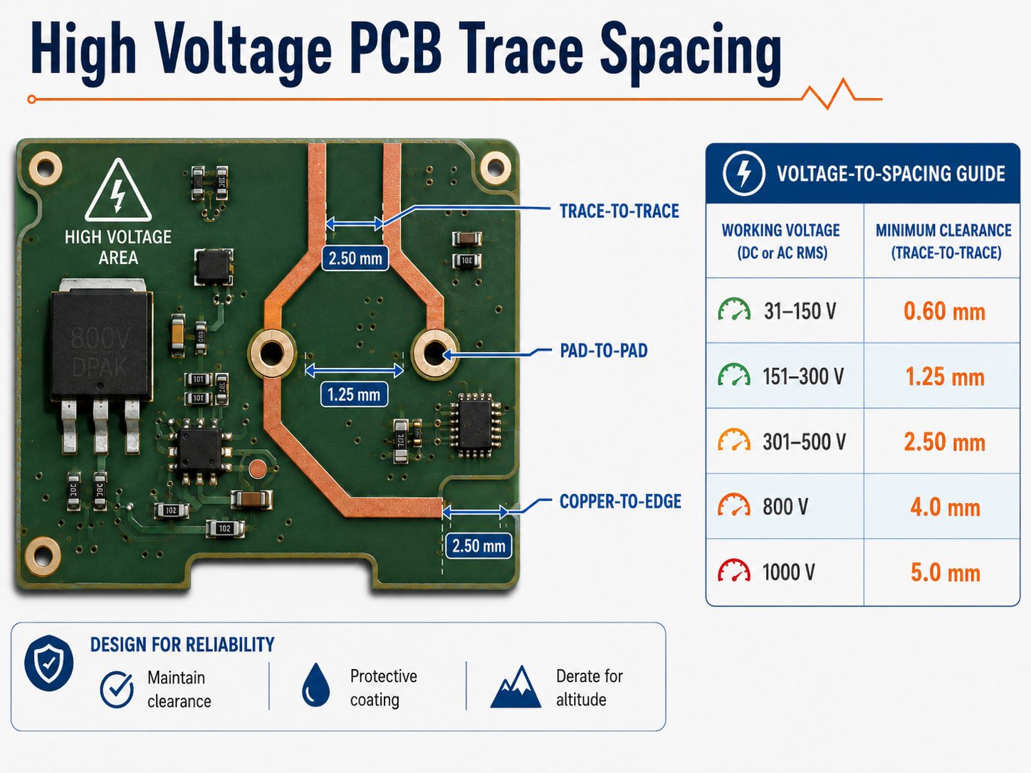
For external uncoated conductors, a useful PCB design reference is approximately 1.25 mm at 151–300 V peak and 2.5 mm at 301–500 V peak; at 1,000 V, the spacing reaches about 5.0 mm under the familiar IPC external-uncoated conductor rule.

A practical reference table is:

Voltage Difference, DC or AC Peak External Uncoated Conductor Spacing
31–150 V 0.60 mm
151–300 V 1.25 mm
301–500 V 2.50 mm
600 V ≈3.0 mm
800 V ≈4.0 mm
1,000 V ≈5.0 mm
High voltage PCB trace spacing infographic with voltage-to-spacing guide

For values above 500 V, the external-uncoated reference increases by approximately 0.005 mm per volt above 500 V.

For example:

1,000 V: 2.5 mm + (500 × 0.005 mm) = 5.0 mm

IPC-2221C is the current IPC-2221 revision. It retains conductor-spacing categories while refining areas such as altitude, vacuum operation, and coating definitions, so the current standard should be checked when establishing released design rules.

These PCB conductor-spacing values should not be treated as the final safety clearance for every product. Medical, mains-powered, industrial, automotive, or reinforced-insulation designs may require greater spacing under their applicable IEC or UL safety standard.

Designers should also check more than trace-to-trace spacing:

  • trace to pad
  • pad to pad
  • copper to board edge
  • trace to mounting hole
  • trace to chassis
  • copper to exposed component lead
  • high-voltage to low-voltage plane
  • outer-layer to inner-layer conductor

The correct design value is the minimum finished-board distance after manufacturing tolerance, not merely the nominal CAD spacing.

Which Materials Are Best for a High Voltage PCB?

High-CTI FR-4 is suitable for many high-voltage PCBs, while specialized high-voltage laminates become more attractive when surface tracking, humidity, thermal stress, or insulation reliability is more demanding.

The most important properties include:

Material Property Why It Matters
CTI Resistance to conductive surface tracking
Dielectric strength Resistance to breakdown through insulation
Moisture resistance Helps preserve insulation in humid environments
CAF resistance Reduces conductive filament reliability risk
Tg Influences thermal dimensional stability
Td Indicates thermal decomposition behavior
Resin system Affects insulation and processing behavior
Z-axis stability Important for multilayer reliability

CTI is not the same as dielectric strength.

Dielectric strength concerns breakdown through the insulating material.

CTI evaluates resistance to conductive tracking across its surface.

This is why two FR-4 materials with similar dielectric strength can require different creepage distances when their CTI classifications differ.

For demanding designs, specifying only “FR-4” is therefore insufficient. The RFQ should identify either the laminate grade or the required CTI, thermal, flammability, and insulation properties.

How Should You Plan the Stack-Up for a High Voltage PCB?

A high-voltage stack-up should first separate HV and low-voltage domains with controlled dielectric thickness, rather than simply adding layers around an existing layout.

The exact dielectric thickness cannot be reduced to one universal number because it depends on the required solid-insulation voltage withstand, laminate system, insulation class, and applicable product standard.

The stack-up should define:

  • dielectric thickness between high-voltage layers
  • high-voltage-to-low-voltage layer separation
  • copper thickness
  • material dielectric properties
  • resin content
  • finished board thickness
  • internal plane clearances
  • via structures crossing voltage domains

Internal copper is surrounded by solid dielectric, so its insulation mechanism differs from exposed surface copper.

Avoid placing a low-voltage or grounded plane immediately underneath a high-voltage node unless the vertical insulation path has been intentionally evaluated.

High-current high-voltage designs need another check. Increasing copper weight can reduce conductor resistance, but heavier copper also changes etching capability, conductor spacing, resin fill, dielectric construction, and finished board thickness.

For unusual HV constructions, stack-up review should therefore happen before final routing, not after the Gerber files are complete.

What Are the Key High Voltage PCB Layout Guidelines?

The most effective layout rule is to create clearly separated HV and LV zones and maintain the required isolation distance around the complete boundary on every copper layer.

Useful layout practices include:

  • Separate HV and SELV/low-voltage areas.
  • Maintain the isolation boundary on every copper layer.
  • Avoid sharp copper points in high-electric-field regions.
  • Use smooth trace and copper transitions where practical.
  • Keep HV copper away from uncontrolled PCB edges.
  • Include vias and plated holes when checking spacing.
  • Avoid unnecessary test points inside HV areas.
  • Keep contamination-sensitive regions accessible for cleaning.
  • Check component body and lead spacing.
  • Prevent copper pours from entering isolation gaps.

A common design error is creating a large visible clearance on the top layer while an internal copper plane extends underneath the same isolation barrier.

Another occurs around components. The traces may meet the intended rule while transformer pins, connector contacts, heat sinks, screws, or component leads create a shorter path.

A high-voltage layout review should therefore inspect the finished electrical assembly, not only individual traces.

When Should You Use Isolation Slots, Barriers, or Conformal Coating?

Use an isolation slot when PCB area is limited and additional creepage is needed; use barriers when the physical insulation path needs to be extended; use conformal coating mainly when environmental contamination or moisture must be controlled.
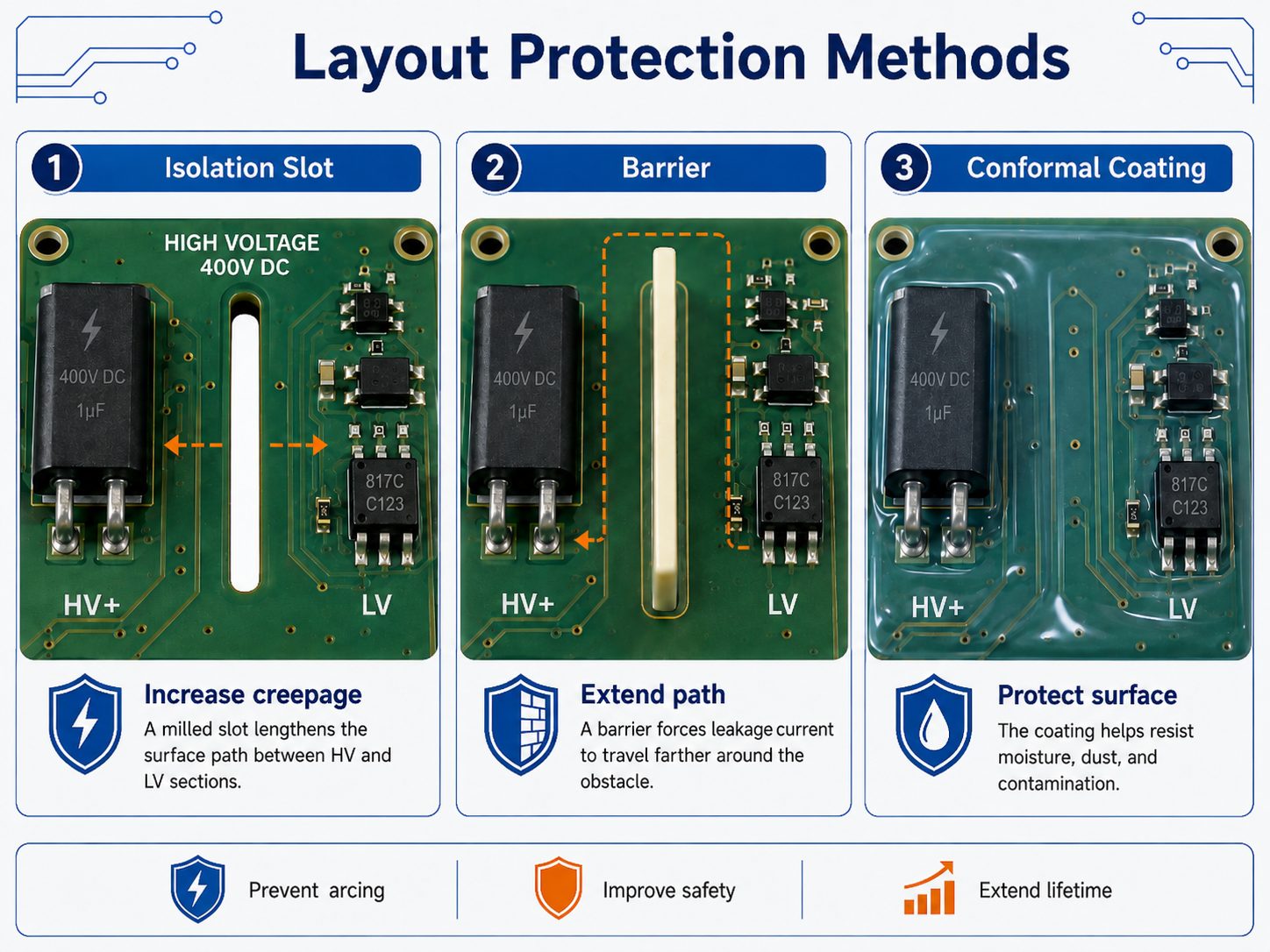
High voltage PCB layout protection methods using isolation slots, barriers, and conformal coating

These three methods solve different problems.

Isolation slots interrupt the direct PCB surface path and can significantly increase creepage without requiring the same increase in board width.

Barriers physically extend or separate insulation paths and may also help prevent contamination from bridging conductive regions.

Conformal coating protects the PCB from humidity, dust, chemicals, and surface contamination.

Coating performance depends on:

  • coating material
  • thickness
  • adhesion
  • coverage
  • cure quality
  • pinholes
  • component shadowing
  • operating environment
  • applicable standard

Do not assume that ordinary solder mask or conformal coating automatically allows a safety clearance to be reduced.

If an isolation slot is safety-critical, specify its finished minimum width, position, and tolerance on the manufacturing documentation rather than relying only on nominal CAD geometry.

Which Standards Apply to High Voltage PCB Design?

For general PCB design, IPC-2221C is a key reference; for insulation coordination, IEC 60664-1 is one of the most important standards, while the final equipment standard determines the binding safety requirement.

Standard Typical Relevance
IPC-2221C Generic printed board design and conductor spacing
IEC 60664-1 Clearance, creepage, insulation coordination
IEC 62368-1 AV and ICT equipment
IEC 60601-1 Medical electrical equipment
UL 796 Printed wiring boards
Product-specific IEC/UL standards Final equipment safety requirements

The key point is that an IPC spacing table does not automatically prove product safety compliance.

A medical device, EV charger, industrial controller, mains power supply, or ICT product may require different insulation levels even if their PCB operating voltages appear similar.

What Manufacturing Factors Matter for High Voltage PCBs?

The most critical manufacturing requirement is that the finished PCB must preserve the minimum insulation distances assumed by the designer after etching, drilling, routing, lamination, and registration tolerances are included.

Key controls include:

  • Copper geometry: etching must not reduce critical spacing.
  • Copper-to-edge distance: routing tolerance must be included.
  • Isolation slots: finished dimensions must meet the required minimum.
  • Dielectric thickness: critical insulation layers must match the approved stack-up.
  • Material control: laminate substitutions require engineering review.
  • Surface cleanliness: ionic contamination can weaken surface insulation.
  • Solder mask registration: misalignment may expose copper.
  • Routing and drilling accuracy: holes and slots can alter creepage paths.
  • Lamination quality: voids and delamination are undesirable in stressed dielectric structures.
  • Traceability: safety-related products may require controlled material and process records.

For example, if a design requires a 2.50 mm finished minimum conductor spacing, drawing two features exactly 2.50 mm apart in CAD leaves no manufacturing tolerance.

This is why high-voltage fabrication notes should clearly distinguish between the nominal design dimension and the minimum finished-board requirement. That distinction helps ensure normal fabrication tolerances do not reduce critical spacing below the required minimum.
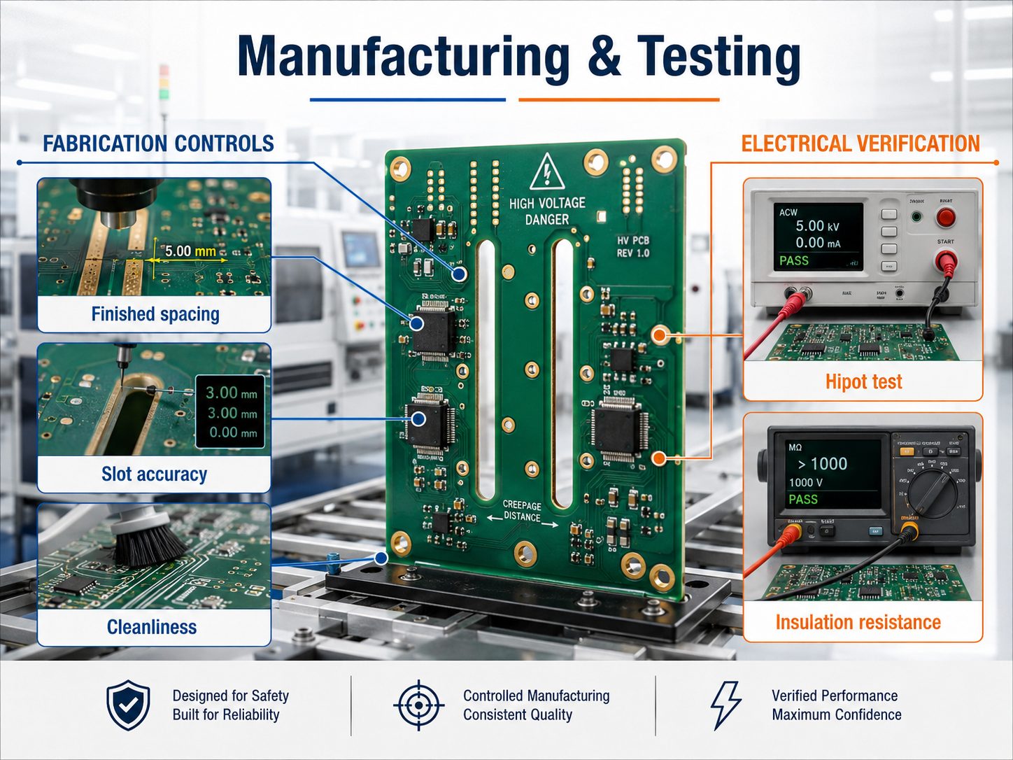
High voltage PCB manufacturing controls and electrical verification including hipot and insulation resistance testing

How Should a High Voltage PCB Be Tested?

At minimum, a high-voltage PCB should receive normal open/short electrical testing; projects with safety-related insulation commonly add insulation-resistance and dielectric-withstand, or hipot, testing according to the product specification.

Depending on the application, verification may include:

  • open/short electrical test
  • insulation resistance test
  • dielectric withstand / hipot test
  • dimensional inspection of isolation gaps
  • isolation-slot inspection
  • cleanliness testing
  • conformal-coating inspection
  • functional testing at operating voltage
  • first-article validation

A hipot test applies a specified voltage between isolated regions and checks whether the insulation can withstand that electrical stress without unacceptable leakage or breakdown.

There is no responsible universal rule such as:

“Test every 1,000 V PCB at 2,000 V.”

The correct hipot voltage and duration come from the end-product standard or approved test specification.

The test document should define:

  • test voltage
  • AC or DC
  • duration
  • ramp rate
  • leakage-current limit
  • test points
  • pass/fail criteria

For assembled boards, PCB-only testing may not be enough. Connectors, component leads, heat sinks, screws, cables, and other hardware can create shorter insulation paths than the bare board itself.

What High Voltage PCB Design Mistakes Should You Avoid?

The most common high-voltage PCB mistake is choosing spacing from nominal operating voltage alone instead of evaluating peak voltage, creepage, clearance, environment, and manufacturing tolerance together.

Other common problems include:

  • Confusing clearance with creepage. Increasing the surface path does not automatically increase the air path.
  • Ignoring altitude. Above approximately 2,000 m, IEC insulation calculations may require clearance correction.
  • Selecting laminate only by dielectric strength. CTI, moisture resistance, thermal behavior, and contamination also matter.
  • Assuming solder mask provides reinforced insulation. This depends on the construction and applicable safety standard.
  • Ignoring internal copper. An outer-layer isolation zone can still contain a hidden plane violation.
  • Leaving sharp copper features in HV regions. Sharp geometry can increase local electric-field concentration.
  • Checking PCB traces but not components. Leads, terminals, heat sinks, connectors, and hardware must also maintain isolation.
  • Designing exactly to the minimum spacing. Fabrication tolerances must be added before design release.

A useful high-voltage design review question is therefore:

Does the finished and assembled product maintain the required insulation under its actual voltage, transient, altitude, contamination, manufacturing tolerance, and service conditions?

FAQs About High Voltage PCB

What voltage is considered high voltage on a PCB?

There is no universal PCB threshold, but approximately 300 V and above is a useful practical point at which clearance, creepage, transients, insulation, and environmental conditions deserve explicit review. Designs in the 300–1,000 V range are common high-voltage PCB territory, while boards above 1 kV are feasible with appropriate engineering.

How much clearance does a high voltage PCB need?

For external uncoated PCB conductors, a useful IPC reference is about 1.25 mm for 151–300 V peak and 2.50 mm for 301–500 V peak, increasing to approximately 5.0 mm at 1,000 V under the external-conductor rule. Product-safety requirements can require larger values.

What is the difference between creepage and clearance?

Clearance is the shortest path through air, while creepage is the shortest path along an insulating surface.

Is FR-4 suitable for high voltage PCBs?

Yes. High-CTI FR-4 is suitable for many 300–1,000 V-class PCB applications, provided its CTI, dielectric construction, thermal performance, creepage, clearance, and end-product requirements are appropriate.

Does conformal coating increase voltage isolation?

It can improve environmental protection and surface insulation performance, but it does not automatically justify smaller safety spacing. The coating material, coverage, process qualification, and applicable standard must support the reduction.

How does altitude affect PCB clearance?

Clearance normally increases with altitude because air density decreases. Above approximately 2,000 m, the applicable standard may require an altitude correction factor.

Can isolation slots increase creepage distance?

Yes. A correctly placed slot can substantially increase creepage without requiring the same increase in PCB width, although clearance must still be checked separately.

If you are developing a high-voltage PCB and want the fabrication capability checked before prototype release, send your Gerber files, stack-up, working voltage, peak or surge voltage, copper weight, material requirements, critical isolation dimensions, and applicable standard to sales@bestpcbs.com. EBest Circuit can review stack-up manufacturability, critical spacing, isolation slots, copper geometry, dielectric construction, and other fabrication-sensitive features before quotation and production.
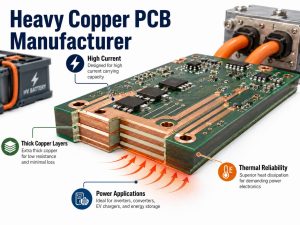
You may also like

High Voltage PCB Design, High Voltage PCB Design Suppliers
Tuesday, June 3rd, 2025

Ever wondered how high voltage PCB design ensures safety and performance? This guide covers rules, supplier selection, and real-world case studies for industrial applications.

EBest Circuit (Best Technology) stands out as a premier high voltage PCB design supplier by directly addressing critical industry pain points. Our key advantage lies in ‌free DFM analysis‌, eliminating costly redesigns by detecting high-voltage creepage errors, material mismatches, and thermal hotspots before production. With ‌IPC-2221A-compliant design rules‌, we resolve arcing risks through optimized 8-layer stack-ups and >3mm clearance guarantees for 10kV+ applications. Clients gain access to ‌real-time impedance simulation tools‌ and ‌CTI>600-rated material libraries‌ to prevent dielectric breakdown. For urgent needs, we offer ‌72-hour prototyping‌ with full Hi-Pot testing data. Case studies include medical imaging PCBs (15kV) with 0% field failures over 5 years. Every design undergoes ‌automated DRC checks‌ for IPC-6012 Class 3 compliance, while our US/EU-trained engineers provide 24/7 support to fast-track UL certification. Welcome to contact us today if you have any request for high voltage PCB design: sales@bestpcbs.com.

What Is High Voltage PCB Design?

High voltage PCB design is a specialized area of printed circuit board development that deals with the creation of boards capable of handling elevated electrical potentials. These boards are integral to various systems where standard voltage levels won’t suffice, such as in power transmission equipment, industrial machinery, and certain medical devices. Compared to standard FR4 PCB design, high voltage PCB design demands increased insulation (e.g., thicker solder masks, higher-quality FR4 materials), wider component spacing to prevent arcing, and careful selection of materials with higher dielectric strength to ensure safe, reliable operation under high voltage conditions.

High Voltage PCB Design

What Are Rules in High Voltage PCB Designs?

  • Clearance Requirements: Guarantee an adequate distance between conductive traces, vias, and components. This spacing is determined by the operating voltage and environmental conditions. For example, higher voltages necessitate greater separation to prevent arcing and electrical breakdown.
  • Insulation Material Selection: Select appropriate insulation materials with high dielectric strength. Materials such as FR – 4 with enhanced dielectric properties can provide better protection against electrical leakage.
  • Trace Width and Thickness: Design traces with sufficient width and thickness to handle the high current in high – voltage applications. Thicker traces reduce resistance and minimize heat generation.
  • Ground Plane Design: Create a robust ground plane to serve as a stable reference point and reduce electromagnetic interference. A well – designed ground plane effectively dissipates electrical noise.
  • Component Placement: Arrange high – voltage components to minimize the risk of electrical stress on other components. Avoid placing sensitive components close to high – voltage sources.
  • Testing and Verification: Implement comprehensive testing procedures, including high – voltage testing, to ensure that the PCB meets the required safety and performance standards.
High Voltage PCB Design

High Voltage PCB Design Guidelines

Below are guidelines about how to design high voltage PCB:

  1. Understand the Application Requirements
  • Voltage Range: Begin by determining the exact voltage levels the PCB will handle, including peak and continuous voltages. For example, if it’s for a power supply application that needs to step up from 12V to 500V, account for transient spikes that might reach 600V or more. Measure the voltage tolerance of each component and ensure the PCB layout can handle these levels without arcing or breakdown.
  • Current Capacity: Calculate the maximum current the circuit will carry. This impacts the width of traces; thicker traces are required for higher currents to reduce resistance and prevent overheating. Use the IPC-2152 standard to calculate the minimum trace width based on the current and temperature rise requirements.
  • Environmental Factors: Consider the operating environment. In a high – humidity setting, use conformal coatings to protect against moisture – induced corrosion. In a high – altitude application, account for the reduced air density, which can lower the breakdown voltage of air gaps, and increase the spacing between high – voltage components accordingly.
  1. Follow Industry Standards
  • IEC Standards: For example, IEC 60664 – 1 defines the insulation coordination for equipment within low – voltage systems. When designing a high – voltage PCB, ensure that the insulation distances between live parts and the creepage and clearance distances meet the requirements specified in this standard. This includes maintaining appropriate distances between traces, vias, and components to prevent electrical breakdown.
  • UL Regulations: UL 1950, for information technology equipment, sets safety requirements. Adhere to these when designing PCBs for devices like servers or data centers with high – voltage power supplies. Test the PCB for compliance with UL’s safety requirements, such as flammability resistance of materials used.
  1. Use Simulation Tools
  • Software Selection: Popular circuit simulation tools like PSpice or Saber can be used. For high – voltage PCB design, these tools can model the behavior of components under different voltage and current conditions. For example, simulate the performance of a high – voltage capacitor in a resonant circuit to check for voltage spikes and ensure its safe operation.
  • Fault Simulation: Run simulations to mimic potential faults, such as a short – circuit between two high – voltage traces. Analyze how the circuit responds and whether it can withstand the fault without causing a catastrophic failure. Use the simulation results to modify the design, such as adding additional protection components or adjusting trace routing.
  1. Consider Thermal Management
  • Heat Sink Design: Select a heat sink with an appropriate thermal resistance based on the power dissipation of the high – voltage components. Calculate the power dissipated in components like high – voltage transistors using the formula P=VI, where V is the voltage across the component and I is the current through it. Ensure proper thermal interface materials, such as thermal paste or pads, are used to improve heat transfer between the component and the heat sink.
  • Thermal Vias: Incorporate thermal vias in the PCB layout. These vias connect different layers of the PCB, allowing heat to be conducted away from high – power components more effectively. Place thermal vias in a grid pattern around the component to evenly distribute the heat across the PCB layers.
  1. Design for EMC Compatibility
  • Shielding: Use conductive shielding materials, such as copper or aluminum foils, to enclose sensitive high – voltage components or sections of the PCB. Connect the shielding to the ground plane at multiple points to ensure effective grounding. For example, shield a high – frequency oscillator on the high – voltage PCB to prevent its electromagnetic emissions from interfering with other parts of the circuit.
  • Grounding Techniques: Establish a solid ground plane. Use star – grounding for sensitive circuits to minimize ground loops and reduce electromagnetic interference. Connect all high – voltage return paths to the ground plane in a controlled manner, ensuring that the ground impedance is kept low.
  1. Documentation
  • Component Specifications: Document the detailed specifications of each component used, including the manufacturer, part number, voltage rating, current rating, and any other relevant characteristics. This information is crucial for component replacement and ensuring the continued safety and performance of the PCB.
  • Design Calculations: Record all design calculations, such as trace width calculations, insulation distance calculations, and power dissipation calculations. This allows for easy verification of the design and provides a basis for future modifications.
  • Test Results: Keep a record of all tests performed on the PCB, including electrical tests (such as voltage withstand tests, insulation resistance tests), thermal tests, and EMC tests. Note any failures and the corrective actions taken.
  1. Iterative Design Process
  • Testing Phases: Conduct multiple rounds of testing, starting with bench – top testing of individual components and sub – circuits, followed by full – system testing. Analyze the test results carefully, looking for any signs of component failure, performance degradation, or safety issues.
  • Feedback Incorporation: Based on the test results and feedback from other engineers or end – users, make iterative changes to the design. This could involve modifying the component layout, changing component values, or adjusting the thermal management or EMC – related design features. Continuously repeat the testing process after each iteration until the high – voltage PCB meets all the design requirements.

High Voltage PCB Design Considerations

  • Select suitable high-voltage components: give priority to electronic components with rated voltages that meet high-voltage working conditions to avoid device failure due to voltage overload, such as high-voltage ceramic capacitors, high-voltage MOSFETs, etc.
  • Reasonable derating: design high-voltage components with derating, such as controlling the operating voltage of components to 60%-80% of the rated voltage to cope with voltage surges and fluctuations and improve long-term stability.
  • Strictly control welding process: use high-reliability welding technology (such as wave soldering, reflow soldering) to ensure that the solder joints are full and there is no virtual solder joints, and prevent local overheating or arcing due to poor contact.
  • Optimize line layout: accurately plan the routing, maintain sufficient line spacing (recommended ≥2mm/kV), avoid parasitic capacitance caused by parallel long routing, and physically isolate high-voltage lines from low-voltage lines.
  • Strengthen insulation design: select PCB substrates with high insulation performance (such as FR-4 high TG materials), increase the thickness of the insulation layer, spray three-proof paint or add insulating potting glue when necessary.
  • Reserve heat dissipation space: For components that are prone to heat under high voltage (such as power resistors and IGBT modules), design heat dissipation copper foil or install heat sinks to ensure that the operating temperature is lower than the critical value of the components.
  • Consider environmental factors: In high humidity environments, use moisture-proof coatings; when dealing with temperature fluctuations, choose materials with low temperature coefficients to prevent thermal stress from causing PCB cracking.
  • Perform test verification: After the design is completed, perform voltage withstand tests (such as 1.5 times the rated voltage), insulation resistance tests, and environmental aging tests to ensure compliance with safety standards.

What Are Common Issues of High Voltage Power Supply PCB Design?

Electrical Breakdown

  • Cause: Insulation failure between conductive elements due to insufficient clearance (e.g., less than the recommended 5mm for high voltage), low – quality insulation materials, or high humidity.
  • Solution: Maintain a minimum clearance of 5 – 10mm between high – voltage traces and components, and use FR – 4 materials with a dielectric strength of at least 14 kV/mm.

Overheating

  • Cause: Narrow traces (less than 0.5mm width for high – current paths) and inadequate cooling.
  • Solution: Use traces with a width of 1 – 2mm for high – current paths, install aluminum heat sinks with a thermal resistance of ≤2.5°C/W, and increase the number of thermal vias to 10 – 15 per square inch.

Electromagnetic Interference (EMI)

  • Solution: Encase the PCB in a metal shield with a conductivity of at least 50% IACS, implement a star – grounding system, and insert ferrite bead filters at the power input.

Component Failure

  • Solution: Select components with a voltage rating 1.5 – 2 times the operating voltage and a current rating 2 – 3 times the maximum load current. Use reflow soldering with a peak temperature of 245 – 255°C for proper joint formation.

Leakage Current

  • Solution: Employ PTFE – coated substrates with a leakage current density of <1μA/cm² and ensure all insulation layers have a thickness of at least 0.2mm.

Voltage Spikes

  • Solution: Place metal – oxide varistors (MOVs) with a clamping voltage 1.2 – 1.3 times the rated voltage at the power input and output of the PCB.

Insulation Degradation

  • Solution: Use silicone – based conformal coatings with a dielectric strength of 20 – 25 kV/mm and inspect the PCB for signs of insulation damage every 6 – 12 months.

Poor Signal Integrity

  • Solution: Route high – speed signals on inner layers with a 50 – ohm impedance, use series – terminating resistors (22 – 33Ω) at the source end of the traces, and add buffer amplifiers for long signal paths.

Inadequate Grounding

  • Solution: Design a solid ground plane covering at least 80% of the PCB area, and use multiple vias (3 – 5 per connection) to connect different ground layers.

Thermal Expansion and Contraction

  • Solution: Use PCBs made of polyimide materials with a coefficient of thermal expansion (CTE) of 15 – 20 ppm/°C and choose components with a similar CTE range.
High Voltage PCB Design

How to Choose High Voltage PCB Design Suppliers?

Here are methods about how to choose high voltage PCB design suppliers:

Experience and Expertise

  • Prioritize suppliers with at least 3 – 5 years of dedicated high voltage PCB design experience. Review their portfolio for projects similar in voltage rating (e.g., >1000V), complexity, and application (such as power electronics or high – energy physics). Request case studies demonstrating how they resolved design challenges like creepage and clearance issues.

Technical Capabilities

  • Confirm that suppliers use industry – standard design tools like Altium Designer with high voltage design libraries. Their manufacturing processes should support high – precision techniques, such as controlled impedance routing and multi – layer PCB fabrication. Ask for details on their testing facilities, including the availability of high voltage testers and thermal cycling chambers.

Quality Assurance

  • Verify that suppliers follow ISO 9001 quality management systems. They should provide detailed inspection reports for each production batch, including visual inspection, X – ray inspection for internal connections, and functional testing results. Ensure they can offer certificates of compliance with relevant high voltage standards, such as IEC 60664 for electrical insulation coordination.

Cost – Effectiveness

  • Obtain quotes from a minimum of 3 suppliers, comparing not only the unit price but also the overall cost structure. Consider factors like tooling costs, setup fees, and potential volume discounts. Evaluate the cost – to – performance ratio by assessing the quality of materials used (e.g., high – voltage – rated laminates) and the expected lifespan of the PCBs.

Delivery Time

  • Select suppliers who can provide a detailed production schedule at the quotation stage, breaking down the time for design review, fabrication, assembly, and testing. Look for a lead time that aligns with your project timeline, with a buffer of at least 10 – 15% to account for potential delays. Confirm their ability to expedite orders if necessary, and inquire about any associated rush fees.

Customer Support

  • Choose suppliers with a dedicated project manager for high voltage PCB design. They should offer 24/7 emergency support channels for critical issues and provide regular progress updates during the design and manufacturing process. Check if they have a technical support team capable of assisting with design optimizations and troubleshooting post – production.

Reputation

  • Research suppliers on industry – specific platforms like PCB Directory or EIPC. Read reviews from clients who have worked on high voltage projects, paying attention to feedback on design accuracy, communication, and problem – solving. Request references and directly contact past clients to inquire about their experience with the supplier.

Flexibility

  • Prioritize suppliers who can accommodate design changes within 24 – 48 hours of request. They should have a change order management system in place, clearly defining the impact on cost and delivery time. Ensure they can handle iterative design processes, which are common in high voltage PCB development due to strict safety and performance requirements.

Certifications

  • Ensure suppliers hold relevant certifications, such as ISO 13485 for medical – grade high voltage PCBs (if applicable) or UL 796 for printed wiring boards. These certifications should be up – to – date and available for verification. Additionally, look for industry – specific certifications, like those from the Institute of Electrical and Electronics Engineers (IEEE) for high voltage engineering standards compliance.

Supply Chain Management

  • Suppliers should have a diversified network of component suppliers, especially for high voltage – specific components like high voltage capacitors and resistors. They should be able to provide a bill of materials (BOM) with alternative part numbers in case of shortages. Request information on their inventory management system to ensure they can maintain a sufficient stock of key materials to meet production schedules.
High Voltage PCB Design Suppliers

How to Verify Your High Voltage PCB Design?

  • Electrical Testing: Conduct comprehensive electrical tests, including high voltage testing, continuity testing, and insulation resistance testing. These tests can identify any electrical faults or weaknesses in the design.​
  • Thermal Testing: Use thermal imaging and other thermal testing methods to measure the temperature distribution on the PCB. This helps in detecting any hotspots and ensuring proper thermal management.​
  • EMC Testing: Perform electromagnetic compatibility testing to ensure the PCB does not emit excessive electromagnetic radiation and is not susceptible to external interference.​
  • Mechanical Testing: Check the mechanical integrity of the PCB, including the strength of the board, the durability of the components, and the reliability of the connections.​
  • Functional Testing: Test the functionality of the high voltage PCB in a real – world or simulated environment to ensure it meets the required performance specifications.​
  • Simulation Verification: Compare the simulation results with the actual test results to verify the accuracy of the design models. This can help in improving future designs.​
  • Documentation Review: Review all the design documentation to ensure it is complete, accurate, and in compliance with the relevant standards and requirements.​
  • Component Verification: Verify the specifications and performance of all the components used on the PCB. This includes checking for proper component selection, correct installation, and compliance with the design requirements.​
  • Design Rule Check (DRC): Run a DRC on the PCB design to ensure it adheres to the established design rules, such as clearance, trace width, and via size requirements.​
  • User Acceptance Testing: If possible, involve end – users in the testing process to get their feedback on the usability and performance of the high voltage PCB.

Do You Have Case Studies of High Voltage PCB Designs for Industrial Applications?

Case Study: High-Power Motor Control PCB for Industrial Robotics

Industry: Industrial Automation

Challenge:
A leading robotics manufacturer required a robust PCB to control two high-torque DC motors (15A each, 30A total) for a precision CNC machine. Key challenges included:

  • Withstanding voltage spikes up to 600V during motor start/stop cycles.
  • Maintaining thermal stability in a 24/7 operation environment.
  • Ensuring electromagnetic compatibility (EMC) to avoid interference with nearby sensors.

Solution:

Material Selection:

  • Used 2oz copper PCB with FR4 substrate (dielectric strength >300V/mil) for reliable insulation.
  • Applied ceramic-filled solder mask to enhance arc resistance and thermal conductivity.

Thermal Management:

  • Integrated 74651195R 85A screw terminals for power input and 30A snap-in connectors for motor outputs to minimize contact resistance.
  • Added 1000μF electrolytic capacitors to suppress voltage transients and stabilize the power rail.
  • Incorporated thermal vias and a 2mm copper ground plane to dissipate heat efficiently.

Safety & Compliance:

  • Implemented dual fuses (30A input, 15A output) and an NTC thermistor for real-time thermal shutdown.
  • Maintained 8mm creepage distance and 6mm air gap between high-voltage (HV) and low-voltage sections, exceeding IPC-2221B standards.

EMC Mitigation:

  • Designed a pi-filter network (10μH inductor + 100nF/1kV capacitor) to attenuate motor noise.
  • Routed HV traces on inner layers to reduce radiated emissions.

Result:

  • Achieved 98% efficiency with zero arc-over incidents during 1000-hour stress testing.
  • Thermal imaging showed a 25°C temperature reduction compared to conventional layouts.
  • Passed IEC 61000-4-4 ESD and EN 55032 EMC certifications on the first attempt.

Conclusion

In conclusion, high voltage PCB design demands specialized technical know-how, practical experience, and meticulous attention to detail. Mastery of design rules, guidelines, and key considerations is the foundation for crafting reliable, efficient high voltage PCBs. From troubleshooting common issues, selecting the right suppliers, to rigorous design verification—each step is non-negotiable. Our case studies showcase real-world applications across diverse industries. Ready to bring your high voltage PCB project to life? Contact sales@bestpcbs.com for a quote. Let our expertise deliver the high-quality design solutions you need.

You may also like