

There are many places in the Printed Circuit Board Design that need to consider the safety spacing, here we summarized Eight Safety Spacings in total to show you what spacing we should pay attention to when designing, they can be separated into two categories, one is Electrical-Related Safety Spacing, and another is Non-Electrical-Related Safety Spacing.
Electrical-Related Safety Spacings
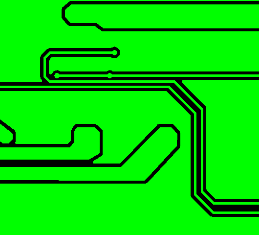
- Wire Spacing
As far as the processing capability of the mainstream PCB manufacturer is concerned, the spacing between the wires shall not be less than 0.075mm. The minimum line distance refers to line to line, line to pad space. From a production perspective, the larger the better, and the more common wire spacing is 0.25mm by far.
- Diameter and Width of Pad
From the processing capability of mainstream PCB manufacturers, the minimum diameter shall not less than 0.15mm if the holes on pad requires mechanically drilled. If used laser drilling, then hole diameter must greater or equal than 0.10mm. At the same time, the tolerance of hole diameters varies slightly according to different substrates. Generally, it can be controlled within 0.05mm, and the minimum width of the pad should not be less than 0.2mm.
- Spacing between Pad to Pad
The spacing between pads must be at least 0.2mm as far as the processing capacity of mainstream PCB manufacturers concerned.
- Copper and Edge of the Board Spacing
The spacing between electronic copper and edge of the board should be no less than 0.30mm, and it can be set spacing rule on the “Design – Rules – Board outline” page.
If it requires a larger area of copper, it is generally needs to set 0.5mm as a retraction spacing from the edge of board. In the PCB design and manufacturing industries, engineers often shrink the large area of copper coating to the edge of the board by 20mil for mechanical considerations of the finished circuit board, or to avoid the occurrence of curling or electrical short circuit caused by the exposure of copper on the edge of the board, rather than coating whole copper to the edge of the board.
There are many methods to handle such shrink problems, such as drawing a keepout layer and then set a distance between copper and the keepout. As a professional PCB manufacturer that have rich experience over 16years, there is a much easy way to set different safety spacings for copper objects. For example, the safety spacing of the whole board set as 0.25mm, then we can set copper to 0.5mm, which can achieve a shrink distance of 0.5mm, and the dead copper that may cause in some devices also can be removed as well.
Non-Electrical-Related Safety Spacing
- Width, Height and Spacing of Legends
We can’t make any changes during the processing of text legend film, except that the line width of legend with D-CODE less than 0.22mm (8.66mil) is enlarged to 0.22mm, that is, the line width of legends L=0.22mm (8.66mil).
The width of the whole charact legends W=1.0mm, the height of the whole legends H=1.2mm, the spacing between the legends D=0.2mm. When the text is less than the above standard, the text legends after printing will be blurred.
- Spacing between Via to Via
The spacing between vias to vias is preferably not less than 8mil.
- Spacing between Legend to Pad
Legends/Silkscreens are not allowed on the pads, otherwise, the covered area can’t be tinned and which will affect the assembly process finally. Generally, manufacturer requires a 8mil space to convenient for silkscreen printing, but if your PCB is small and limited in area, it is barely acceptable to leave a 4 mil safety space.
If some legends accidentally over the pads in your design, EBest Circuit (Best Technology) will remove or move to another area when get your approval to ensure good tinned.
Of course, design on a case-by-case situation. Sometimes the screen printing is deliberately close to the pad, because when the two pads are very close, the screen printing in middle can effectively prevent the short circuit of the solder connection during soldering, and this is another case.
- Mechanical 3D height and Horizontal Spacing
When mounting the components on the PCB surface, it is necessary to consider whether there will be conflicts with other mechanical structures in horizontal direction and spatial height. Therefore, in the PCB design, the compatibility between components, finished products and product outer house and spatial structure should be fully considered, and the safety spacing should be reserved for each target object to ensure there is no conflicts occur in space.
In summary, there are many data and key points should be pay highly attention to while in PCB designing, EBest Circuit (Best Technology) manufactures varies of good quality PCBs for our customers, so please do not hesitate to contact us when you have PCB design, we can help to evaluate it freely for you.
You may also like


Tags: FR4 PCB