PCB manufacturing PCB manufacturing
Home > Blog

Edge Connector PCB

PCB Beveling Guide for Gold Finger and Edge Connector Boards
Thursday, June 4th, 2026

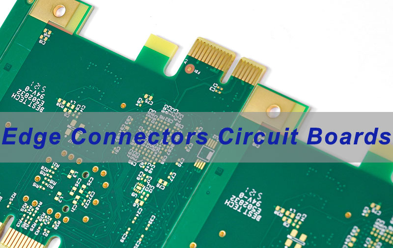
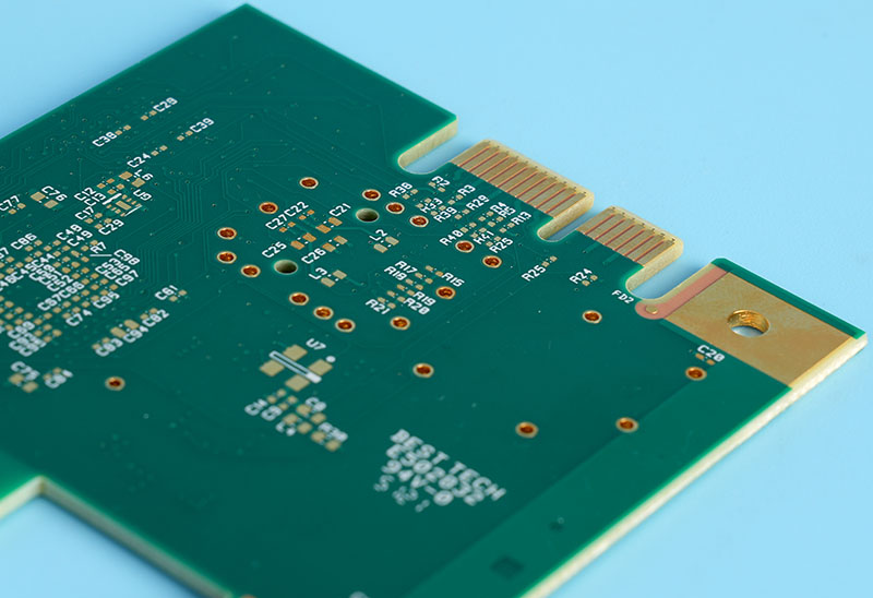
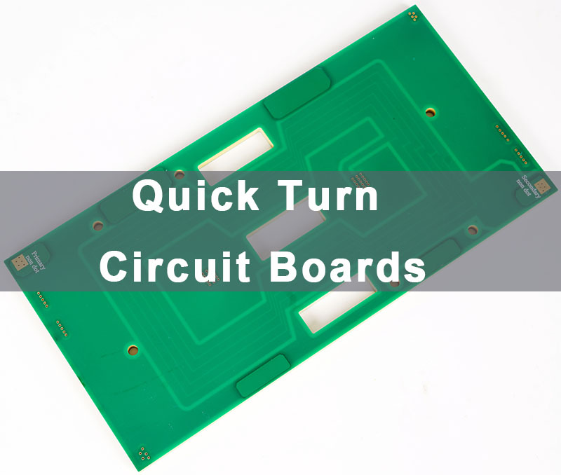
PCB beveling is a board-edge machining process used to create an angled edge on a printed circuit board. It is especially important for gold finger PCBs, edge connector boards, edge card PCBs, plug-in modules, and other boards that need to slide into a connector smoothly. A well-controlled PCB bevel edge can improve insertion, reduce connector wear, protect the gold finger area, and support more consistent assembly in production.

EBest Circuit (Best Technology) supports PCB fabrication, PCB beveling, gold finger processing, DFM review, PCB layout manufacturability feedback, PCBA assembly, testing, and shipment documentation. If you need PCB beveling for gold finger boards, edge connector boards, or batch PCB panels, you can send your available files to sales@bestpcbs.com for engineering review.

PCB Beveling

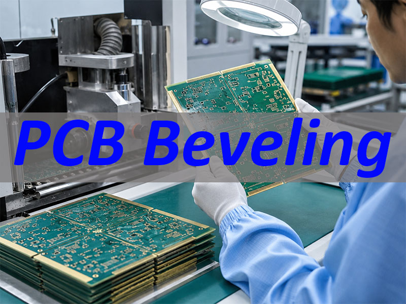
What Is PCB Beveling?

PCB beveling is the process of cutting or grinding the edge of a PCB into a sloped surface instead of leaving it as a straight 90-degree edge. This angled edge helps the board enter a connector more smoothly.

It is commonly used for:

  • Gold finger PCB
  • Edge connector PCB
  • Edge card PCB
  • Plug-in control boards
  • Communication modules
  • Industrial cards
  • Test boards
  • High-volume PCB panels requiring edge finishing

A PCB beveler is the machine or tool used to create this angled edge during PCB manufacturing. In most projects, the customer does not need to specify the machine itself. What matters more is the bevel angle, bevel side, bevel depth, board thickness, copper clearance, and gold finger location.

PCB beveling is different from normal routing or profiling. Routing defines the board outline. Beveling creates a controlled angled edge in a specific area, usually near the connector side.

PCB Beveling

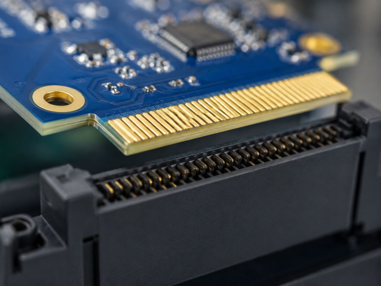
Why Do Gold Finger and Edge Connector PCBs Need Beveling?

Gold finger and edge connector PCBs often need repeated insertion into sockets or card-edge connectors. Without beveling, the board edge may feel too sharp, create friction, or interfere with smooth connector insertion.

PCB gold finger beveling helps with:

  • Smoother insertion
    • The angled edge guides the board into the connector.
    • It reduces resistance during plugging.
  • Lower connector wear
    • A sharp PCB edge may scratch or stress the connector.
    • A beveled edge improves contact handling.
  • Better gold finger protection
    • Proper beveling helps reduce mechanical impact on the plated contact area.
    • It supports stable mating between the PCB and connector.
  • Cleaner assembly
    • Plug-in boards are easier to install.
    • Operators can insert the board with less force.
  • More consistent product experience
    • This is useful for industrial cards, communication boards, control modules, and other plug-in electronic products.

For edge card bevel PCB projects, beveling is not only a cosmetic process. It affects connector fit, insertion feel, long-term contact reliability, and production handling.

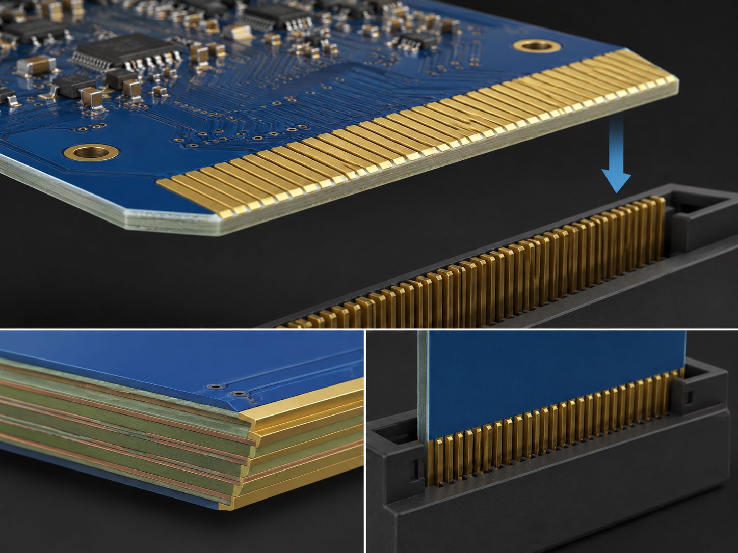
What Is a PCB Beveled Edge?

A PCB beveled edge is the angled part of the board edge after beveling. It is usually located on the connector side of the PCB, especially where gold fingers are placed.

A beveled edge may be required on:

  • One side of the board edge
  • Both sides of the board edge
  • Only the gold finger edge
  • A defined section of the PCB outline
  • Individual boards or full panels before separation

Important points to confirm:

  • Which edge needs beveling?
  • Is the bevel on the top side, bottom side, or both sides?
  • What bevel angle is required?
  • What bevel depth or remaining thickness is required?
  • Is there enough copper clearance from the board edge?
  • Will the bevel affect gold finger contact length?
  • Should the beveled edge be processed before or after surface finish?

Not every PCB edge should be beveled. For boards with copper close to the edge, plated slots, castellations, edge plating, or special mechanical structures, the beveling area should be reviewed before production.

EBest Circuit (Best Technology) can review the customer’s mechanical drawing and existing PCB layout files to check whether the bevel edge is manufacturable. This is part of DFM and layout manufacturability feedback, not original PCB design service.

What Bevel Angle Is Common for PCB Edge Connectors?

PCB bevel angle should follow the customer’s mechanical drawing or connector requirement. Commonly requested bevel angles include 20°, 30°, and 45°, depending on the connector structure, board thickness, insertion direction, and product requirement.

Common bevel angle considerations:

  • 30° bevel
    • Often used for edge connector and gold finger PCB projects
    • Provides a moderate lead-in edge for insertion
  • 45° bevel
    • Common for stronger edge chamfering
    • Useful when the connector or mechanical structure allows it
  • 20° bevel
    • Used in some plug-in applications
    • May require more specific mechanical confirmation

Before production, the following points should be confirmed:

  • Bevel angle
  • Bevel side
  • Bevel length
  • Bevel depth
  • Finished board thickness
  • Gold finger length
  • Connector requirement
  • Copper-to-edge clearance

A reliable PCB beveling process should not rely on guesswork. If the bevel angle, bevel direction, or bevel depth is unclear, EBest Circuit (Best Technology) can raise an engineering question before production. This helps avoid mismatch between the PCB edge and the customer’s connector.

What PCB Beveling Capabilities Does EBest Circuit (Best Technology) Offer?

For PCB beveling projects, customers usually care about edge quality, angle control, gold finger protection, batch consistency, and whether the supplier understands connector-side requirements. EBest Circuit (Best Technology) supports PCB beveling for gold finger boards, edge connector boards, and batch PCB panels.

Key PCB beveling capabilities include:

  • Gold finger beveling
    • Suitable for gold finger PCB and edge connector PCB
    • Helps improve plug-in performance and connector fit
  • Common bevel angle support
    • Supports common beveling requirements such as 20°, 30°, and 45°
    • Other bevel angles can be reviewed according to project drawings
  • Bevel side control
    • Single-side beveling
    • Double-side beveling
    • Defined-edge beveling based on mechanical drawings
  • Bevel depth control
    • Reviewed according to board thickness and connector requirement
    • Helps avoid excessive cutting into the contact area
  • Gold finger area protection
    • Checks bevel location against gold finger area
    • Helps reduce scratch, burr, and plating damage risk
  • Copper clearance review
    • Reviews copper distance from board edge
    • Helps avoid exposed copper after beveling
    • Useful for multilayer boards with inner copper close to the edge
  • Batch panel beveling
    • Supports panel-level beveling review
    • Suitable for prototype, small batch, and volume production
  • Outgoing quality check
    • Edge smoothness
    • Burr control
    • Chipping check
    • Exposed copper check
    • Visual inspection before shipment

EBest Circuit (Best Technology) reviews beveling requirements together with board thickness, surface finish, gold finger design, panel format, and assembly needs. This helps ensure the board is not only fabricated correctly, but also ready for connector insertion and downstream assembly.

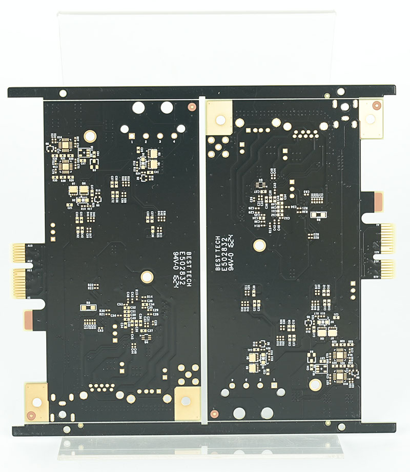
How Are PCB Panels Beveled in Batch Production?

Batch PCB panel beveling is different from beveling one or two sample boards. When a customer has hundreds or thousands of laminate panels or PCB panels to be beveled, consistency becomes the main concern.

For batch PCB beveling, the following details should be checked:

  • Panel size
  • Board thickness
  • Quantity
  • Bevel side
  • Bevel angle
  • Bevel length
  • Surface finish
  • Gold finger location
  • Panel handling method
  • Packaging requirement
  • Outgoing inspection standard

For example, if a customer says, “We have around 4000 laminate panels to be beveled,” the project should not be treated as a simple edge cut. The supplier should confirm whether the panels are bare laminate panels, processed PCB panels, gold finger panels, or assembled boards. Each situation may require different handling.

Key concerns in batch panel beveling:

  • Consistency
    • The bevel angle should remain stable across panels.
    • The edge finish should be uniform.
  • Handling safety
    • Thin or large panels may need careful handling.
    • Panel warpage and edge damage should be controlled.
  • Edge quality
    • Burrs, rough glass fiber, chipping, and exposed copper should be checked.
  • Production efficiency
    • Batch processing should match delivery schedule and packaging requirements.
  • Clear approval before production
    • Manufacturing files and beveling notes should be confirmed before batch release.

EBest Circuit (Best Technology) can review batch beveling requirements before production and confirm whether the project should be processed as individual boards, production panels, or customer-supplied laminate panels.

What Files and Notes Are Needed for PCB Beveling?

Customers do not need to prepare perfect documentation before contacting EBest Circuit (Best Technology). Available files can be sent first, and missing beveling details can be clarified during engineering review.

For an initial PCB beveling review, helpful information includes:

  • Gerber files
  • Drill files
  • Mechanical drawing
  • Board outline
  • Board thickness
  • Bevel edge location
  • Bevel side
  • Bevel angle
  • Quantity
  • Surface finish
  • Panel or single-board delivery requirement

For gold finger or edge connector boards, also provide if available:

  • Gold finger drawing
  • Connector drawing
  • Bevel depth requirement
  • Gold plating requirement
  • Copper clearance requirement
  • Insertion direction
  • Special packaging notes

Practical reminders:

  • If the bevel angle is not marked, it should be confirmed before production.
  • If the bevel side is unclear, an engineering question should be raised.
  • If copper is too close to the board edge, manufacturability should be reviewed.
  • If the board needs SMT assembly, beveling should be checked together with panelization and handling.
  • If the project involves batch PCB panel beveling, panel size and packaging should be confirmed early.

For quotation and manufacturability review, customers can send available files to sales@bestpcbs.com. EBest Circuit (Best Technology) will review the project and advise what extra information is needed before production.

PCB Beveling

FAQs About PCB Beveling

What is PCB beveling?
PCB beveling is a board-edge machining process that creates an angled edge on a PCB. It is commonly used for gold finger boards, edge connector PCBs, and plug-in boards.

What is a beveler in PCB manufacturing?
A beveler is the machine or tool used to create the beveled edge on a PCB. In production, the more important details are bevel angle, bevel side, bevel depth, board thickness, and gold finger location.

Why do gold fingers need beveling?
Gold fingers often connect with edge card connectors. Beveling helps the PCB slide into the connector more smoothly and reduces mechanical wear during insertion.

What is a PCB beveled edge?
A PCB beveled edge is the angled board edge created by the beveling process. It is usually located at the connector side of the board.

What bevel angle is common for PCB edge connectors?
Commonly requested angles include 20°, 30°, and 45°. The final angle should follow the customer’s mechanical drawing or connector requirement.

Is PCB beveling only used for gold fingers?
No. Gold finger beveling is common, but PCB beveling can also be used for edge connector boards, plug-in modules, test cards, and other boards that require smooth insertion or edge finishing.

Can PCB panels be beveled in batch production?
Yes. PCB panels can be beveled in batch production. For large quantities, panel size, board thickness, bevel side, bevel angle, edge quality, and packaging should be confirmed before production.

What files are needed for PCB beveling?
Gerber files, drill files, mechanical drawings, board thickness, bevel angle, bevel side, bevel location, surface finish, and quantity are helpful. If the board has gold fingers, a connector drawing or gold finger drawing is also useful.

Can EBest Circuit (Best Technology) review PCB beveling before production?
Yes. EBest Circuit (Best Technology) can review beveling requirements, gold finger location, copper clearance, board thickness, panel format, and manufacturability before production.

How can I start a PCB beveling quotation?
Send your available files and beveling notes to sales@bestpcbs.com. EBest Circuit (Best Technology) will review the project and confirm whether any additional details are needed.

You may also like

Quick-Turn Edge Connectors Circuit Boards with PCBA Services
Tuesday, January 6th, 2026

Edge connectors circuit boards are specialized printed circuit boards (PCBs) that integrate a row of exposed copper contacts along one edge, designed to mate directly with a corresponding edge connector socket. This blog will explore how these interfaces work, their design nuances, and why choosing a manufacturer offering quick-turn​ production and integrated PCBA services​ is critical for modern electronics development.

What specific challenges do engineers face when working with PCB edge connectors?

  • Prototyping Delays:​ Long lead times for circuit board edge connector​ prototypes stall critical design validation and time-to-market.
  • Design for Manufacturability (DFM) Errors:​ Incorrect PCB edge connector design​ parameters (e.g., gold finger thickness, chamfer) lead to mating failures and costly board respins.
  • Signal Integrity Concerns:​ Poorly designed edgeboard connectors​ on high-speed boards cause signal reflection, crosstalk, and data errors.
  • Mechanical Reliability Issues:​ Weak solder joints or improper card edge connector​ selection result in connection failures under vibration or frequent insertion cycles.
  • Fragmented Supply Chain:​ Sourcing boards from one vendor and PCBA services​ from another complicates logistics, increases cost, and blurs accountability.

Fortunately, these hurdles can be overcome by partnering with a manufacturer like EBest Circuit (Best Technology) that specializes in quick-turn, high-mix production. Our integrated approach provides clear solutions:

  • Accelerated Prototyping:​ We offer rapid quick-turn​ fabrication for edge connectors circuit boards, compressing development cycles from weeks to days.
  • Expert DFM Guidance:​ Our engineering team reviews your printed circuit board edge connector​ design upfront, ensuring optimal gold finger plating, tolerance, and beveling.
  • Controlled Impedance & Stack-up:​ We manufacture boards with precise impedance control for high-speed edge connector PCB​ interfaces, ensuring signal integrity.
  • Robust Assembly Processes:​ Our PCBA services​ include specialized soldering profiles and inspection for reliable card edge connector​ attachment.
  • Single-Source Integration:​ From PCB edge connector design​ to finished assembly, we manage the entire process under one roof, ensuring quality and seamless support.

EBest Circuit (Best Technology) is a specialized PCB and assembly manufacturer focused on delivering high-quality, quick-turn​ solutions for complex applications. We excel in producing reliable edge connectors circuit boards​ with demanding specifications, from single-layer to multi-layer controlled impedance designs. Our in-house PCBA services​ ensure a seamless, accountable workflow from bare board to fully tested assembly. For your next project, pls feel free to contact our experts at sales@bestpcbs.com.

 Edge Connectors Circuit Boards

What Are Edge Connectors Circuit Boards and How Do They Work?

Printed circuit board edge connectors, often called card edge connectors, provide a direct, pluggable interface between a PCB and another system component. This section explains their fundamental operation.

  • The Interface:​ The PCB itself features a row of exposed copper pads or “fingers” plated with hard gold for durability and low contact resistance. This is the male part of the connection.
  • The Socket:​ A corresponding edge connector socket, mounted on a backplane, cable, or another PCB, contains spring-loaded contacts.
  • The Connection:​ When the PCB’s edge is inserted into the socket, the spring contacts press firmly against the gold fingers, establishing a reliable electrical and mechanical connection.
  • Key Advantage:​ This design eliminates the need for a separate connector soldered to the board, saving space, cost, and one soldering step.

In summary, edge connectors circuit boards​ function by using the board’s own substrate and conductive layers as the plug component, creating a simple, compact, and cost-effective interconnect system widely used across electronics.

 Edge Connectors Circuit Boards

How Does a Printed Circuit Board Edge Connector Differ from Traditional Connectors?

Traditional connectors (e.g., pin headers, D-Subs) are discrete components soldered onto the PCB. A circuit board edge connector​ is integral to the board itself. Here’s a breakdown of the key differences:

FeaturePrinted Circuit Board Edge ConnectorTraditional Soldered Connector
Form FactorThe PCB edge is the connector.A separate component mounted on the PCB.
ProfileVery low profile, saves vertical space.Adds height and footprint to the board.
AssemblyRequires plating the board edge; no part soldering.Requires procurement, placement, and soldering.
CostLower part count and simplified assembly.Cost of connector plus assembly labor.
DurabilityMating cycles dependent on PCB plating quality.Mating cycles defined by connector specs.

The choice hinges on design priorities: edge connector PCB​ designs favor space and cost savings, while traditional connectors offer greater flexibility in cable attachment and sometimes higher cycle life.

Common Applications of Circuit Board Edge Connector in Modern Electronics

Edge connector sockets​ and their corresponding boards are ubiquitous due to their reliability and simplicity. Common applications include:

  • Expansion Cards:​ The classic example: PCIe, PCI, and older ISA slots in computers use a card edge connector​ interface.
  • Board-to-Board Connection:​ Board to board edge connector​ setups allow daughterboards to plug perpendicularly or parallel into a main board, common in industrial control systems.
  • Test & Programming Fixtures:Edge connectors circuit boards​ are ideal for test points and device programming jigs, allowing quick insertion and removal.
  • Consumer Electronics:​ Used internally in gaming consoles, appliances, and audio equipment for modular sub-assemblies.
  • Communication Hardware:​ Network routers and switches often use edgeboard connectors​ for modular interface cards.
  • Industrial I/O Modules:​ PLCs (Programmable Logic Controllers) utilize this interface for modular input/output cards.

From a 10 pin circuit board edge connector​ in a simple module to high-pin-count interfaces in servers, this technology enables modular, serviceable, and compact electronic designs.

Understanding Card Edge Connector Types for Different PCB Designs

Selecting the right card edge connector type​ is crucial for mechanical and electrical performance. Key types include:

  • Single/Double-Sided:​ Contacts on one or both sides of the PCB edge.
  • Pitch (Center-to-Center Spacing):​ Common pitches are 2.54mm (0.1″), 2.0mm, and 1.27mm. Finer pitches allow more connections in less space.
  • Pin Count:​ Ranges from few (e.g., 8 position printed circuit board edge connector) to hundreds. A universal 10 pin circuit board edge connector​ is common for simpler I/O.
  • Socket Style:​ Wire-to-board card edge connectors​ have solder tabs or crimp contacts for cables. Card edge connector male​ (the PCB) plugs into a female socket on another board.
  • Tail Type:SMT (Surface Mount) or THT (Through-Hole) for socket mounting.

The choice depends on your PCB edge connector design​ requirements: space constraints, current-carrying needs, required mating cycles, and assembly method for the socket.

Key Considerations for PCB Edge Connector Design

Designing a reliable PCB edge connector​ interface requires attention to detail. Here are the critical factors:

  • Gold Finger Specifications:​ Specify plating thickness (typically 30 µ” gold over 100-200 µ” nickel) and length. A proper chamfer (bevel) on both sides of the edge is mandatory for easy insertion.
  • PCB Thickness:​ This is the most critical dimension. The standard thickness for the connector area is 1.6mm (0.063″), but other sizes (1.2mm, 2.0mm) exist. It must match the socket’s acceptance range exactly.
  • Contact Pad Layout & Spacing:​ Pads must align perfectly with socket contacts. Include solder mask relief and appropriate pad extension beyond the board edge.
  • Mechanical Support:​ For larger boards or high-stress environments, include guide holes or notches for polarization and card edge connector cable​ strain relief.
  • Impedance Control:​ For high-speed signals, the connector PCB edge​ region must be designed with controlled impedance, requiring careful stack-up planning with your manufacturer.

Neglecting these considerations is a leading cause of failure in edge connectors circuit boards, underscoring the need for expert DFM review.

How to Select the Right PCB Card Edge Connector for Your Application?

Follow this decision framework to select the optimal PCB card edge connector​ system:

Define Electrical Needs:​ List the number of signals (pin count), current per pin, voltage, and signal speed (requiring impedance control).

Assess Mechanical Environment:​ Determine mating cycle requirements, board size, insertion/ extraction forces, and exposure to vibration/shock.

Choose the Socket Family:​ Based on #1 & #2, select a standard card edge connector​ family (e.g., DIN 41612, PCIe) or a custom design.

Design the PCB to the Socket Spec:​ Use the socket manufacturer’s datasheet to define your PCB edge connector design—thickness, gold finger layout, tolerances, and bevel.

Partner with a Capable Manufacturer:​ Ensure your PCB/PCBA partner has proven experience producing to these precise mechanical specs. This is where quick-turn​ expertise is invaluable for iterative testing.

Electrical and Mechanical Limits of Edge Connector PCB Interfaces

Understanding the limits of edge connector PCB​ interfaces ensures reliable system performance.

  • Electrical Limits:
    • Current Rating:​ Typically 1-3 A per contact, limited by contact spring material and PCB trace width.
    • Voltage Rating:​ Ranges from 250V to 500V AC/DC, influenced by contact spacing (pitch) and housing material.
    • Signal Speed:​ Traditional designs are limited to a few hundred MHz. For higher speeds, specialized connectors with ground shielding contacts are required to manage impedance and crosstalk.
  • Mechanical Limits:
    • Mating Cycles:​ Commercial connectors rate from 50 to 500 cycles. High-cycle versions use more durable plating and spring designs.
    • Contact Normal Force:​ The spring force (often 50-300g per contact) ensures electrical continuity but creates total insertion force.
    • PCB Durability:​ The hard gold plating on the fingers is wear-resistant, but excessive cycling will eventually wear through to the nickel underplate.

When to Use a Card Edge Connector Socket Instead of Soldered Connections?

Opt for a card edge connector socket​ when:

  • Modularity is Required:​ The board needs to be removable for upgrades, replacement, or field servicing.
  • Space is Constrained:​ Eliminating a bulky connector body saves valuable board real estate.
  • Cost Optimization is Key:​ Reducing component count and assembly steps lowers total cost at high volume.
  • High-Density Interconnection is Needed:​ Edge connectors​ can achieve very high pin density in a linear space.
  • Board-to-Board Stacking:​ For perpendicular connection, an edge connector​ is often the most straightforward solution.

Stick with soldered connectors (like headers) when the connection is permanent, needs extreme durability against frequent mating, or involves direct cable attachment without an intermediate socket.

PCB Capabilities That Matter for Printed Circuit Board Edge Connector Projects

Not all PCB shops can reliably produce printed circuit board edge connectors. Essential capabilities include:

  • Precision Routing & Scoring:​ Ability to hold tight tolerances on board outline and edge connector tab dimensions (±0.1mm or better).
  • Controlled Beveling:​ Automated, consistent chamfering at a precise angle (typically 30°-45°) on the gold finger edges.
  • Selective Plating:​ Expertise in plating the finger area with the correct gold/nickel thickness while avoiding plating on other board areas.
  • Impedance Control:​ For high-speed designs, the ability to model, fabricate, and test controlled impedance traces up to the board edge.
  • Quality Inspection:​ Automated Optical Inspection (AOI) for finger defects and plating quality checks.
  • Quick-Turn Prototyping:​ The agility to produce functional prototypes in days to accelerate design validation.

Why Engineers Choose EBest Circuit (Best Technology) for Edge Connectors Circuit Boards?

Edge connector circuit boards, critical for high-speed data transfer and reliable power delivery in applications from telecommunications to industrial computing, demand manufacturing precision and rigorous quality control. Engineers selecting a partner for these specialized PCBs need a supplier that combines advanced technical capabilities with proven reliability. EBest Circuit (Best Technology) has established itself as a leading choice by consistently delivering on these critical requirements, offering a blend of expert craftsmanship, comprehensive quality assurance, and end-to-end service that ensures connector interfaces perform flawlessly, cycle after cycle.

1. Precision Manufacturing and Gold Finger Expertise

  • Controlled Plating:​ Advanced processes guarantee precise gold finger thickness (0.1 – 1.27µm) with a consistent nickel underlayer, ensuring optimal conductivity, durability, and wear resistance.
  • Exact Beveling:​ High-precision beveling with controlled angles (20°, 30°, 45°, 60°) and depth tolerances (±0.1mm) ensures smooth mating and unmating with the connector socket.
  • Tight Tolerances:​ Strict control over finger spacing, alignment, and geometry prevents signal integrity issues and connection failures.

2. Proven Experience with Complex and Demanding Designs

  • High-Layer Capability:​ Expertise in fabricating complex multi-layer boards (up to 50+ layers) that often incorporate edge connectors, ensuring structural integrity and signal performance.
  • Material Versatility:​ Ability to work with various substrate materials and surface finishes required for high-frequency or high-reliability applications involving edge connectors.
  • Proven Performance:​ A long history of successfully producing boards that meet the stringent demands for insertion cycles and electrical stability in challenging environments.

3. Rigorous Quality Assurance and Reliable Performance

  • Certified Systems:​ Adherence to international quality standards (ISO 9001:2015, IATF 16949:2016) underpins a commitment to consistent, high-quality output.
  • Advanced Testing:​ Comprehensive use of Flying Probe testers, Automated Optical Inspection (AOI), and X-Ray to verify plating integrity, electrical connectivity, and the absence of defects.
  • On-Time Delivery:​ A proven track record of 97% on-time delivery ensures that project schedules are met reliably, reducing time-to-market.

4. Comprehensive Turnkey Service Simplifies Sourcing

  • One-Stop Solution:​ Full-service offering from PCB fabrication and precision plating to component sourcing and assembly, streamlining the entire supply chain.
  • Expert Support:​ Direct access to engineering support for Design for Manufacturability (DFM) feedback, ensuring designs are optimized for reliability and cost-effectiveness from the start.

5. Competitive Value and Responsive Customer Partnership

  • Cost-Effectiveness:​ Optimized manufacturing processes deliver high-quality boards at competitive prices, providing excellent value.
  • Rapid Prototyping:​ Expedited services, including 24-hour turnarounds for prototypes, allow for faster design iteration and validation.
  • Dedicated Support:​ A partnership model with one-on-one sales and engineering assistance ensures responsive and effective communication.

Overall, choosing the right manufacturing partner is just as critical as selecting the right connector architecture when it comes to edge connectors circuit boards. Precision gold finger processing, tight mechanical tolerances, validated materials, and disciplined quality control directly determine long-term reliability, signal integrity, and insertion durability. EBest Circuit (Best Technology) brings these capabilities together with proven experience, certified processes, and fast-turn PCBA support, enabling engineers to move from prototype to production. For projects where performance, schedule, and reliability cannot be compromised, partnering with a manufacturer that understands both the electrical and mechanical demands of edge connector interfaces makes all the difference.

 Edge Connectors Circuit Boards

In a nutshell, edge connectors circuit boards​ provide a streamlined, cost-effective method for creating pluggable interfaces in electronic devices. This blog has explored their operation, design, selection, and the critical manufacturing considerations involved. For success with these specialized PCBs, partnering with a manufacturer possessing the right expertise is essential. EBest Circuit (Best Technology)​ excels in delivering high-quality, quick-turn edge connectors circuit boards​ and integrated PCBA services, ensuring your project benefits from seamless engineering support and reliable production from start to finish. Pls feel free to contact us anytime to discuss your requirements via sales@bestpcbs.com.

You may also like