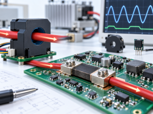
PCB trace length matching keeps related signals within an interface’s permitted arrival-time difference. The matching tolerance comes from the device’s timing requirements and available skew budget, rather than clock frequency alone. Equal copper lengths are useful when they produce the required delay relationship.
Why can equal-length traces arrive at different times, and how much mismatch is acceptable? Routing layers, dielectric properties, vias, and package paths all influence the answer. The practical approach is to identify the correct signal groups, calculate their permitted delay difference, and verify the routes after tuning.
What Is PCB Trace Length Matching?
PCB trace length matching adjusts related routes so their lengths or calculated propagation delays remain within a specified tolerance. Common examples include the two conductors of a differential pair and data signals referenced to a clock or strobe.
Matching means meeting the permitted difference, not achieving perfect geometric equality. Once the routes satisfy their timing constraints, additional tuning can add unnecessary length, bends, and coupling.
Two requirements must be checked separately:
- Maximum path length: Limits the overall connection according to channel or timing requirements.
- Matched length or delay: Limits the difference between related signal paths.
Two traces can match closely while both exceed the permitted channel length. A valid layout must satisfy both requirements.
Which Signals Require PCB Trace Length Matching?
Apply matching where the receiver depends on a defined timing relationship. The device’s hardware design guide establishes which signals belong together and which path acts as the reference.
| Signal Group | Matching Reference | Main Check |
|---|---|---|
| Differential pair | Other conductor in the pair | Intra-pair skew |
| Source-synchronous data | Associated strobe or clock | Data-to-reference timing |
| Synchronous parallel bus | Specified clock and group | Sampling margin |
| Multiple serial lanes | Interface-defined lane relationship | Inter-lane skew |
| Control signals | Reference specified by the device | Device-specified timing limits |
For memory interfaces, a data byte lane may be referenced to its associated strobe. Address, command, and clock signals can follow different rules. Do not place every memory signal in one universal matching group.
Ordinary GPIO and slow control signals usually have other routing priorities. Match them only when their timing requirements establish a relationship with another signal.
How Does PCB Trace Length Mismatch Create Timing Skew?
For routes with comparable structures, the longer path introduces more propagation delay. Their arrival-time difference is the routing contribution to skew.
Routing skew ≈ Length mismatch × Propagation delay per unit length
A 2 mm mismatch at an assumed 6 ps/mm produces approximately 12 ps of routing skew. The actual propagation value depends on the stackup and routing structure.
In a source-synchronous interface, data must remain stable around the sampling edge:
- Setup time: The required stable interval before sampling.
- Hold time: The required stable interval after sampling.
An unsuitable data-to-strobe relationship reduces the available sampling margin. Package paths, connectors, and transmitter timing may contribute further skew, so the comparison must use the endpoints specified by the interface.
How Do Frequency, Data Rate and Rise Time Affect PCB Trace Length Matching?
Frequency, data rate, and rise time describe different signal properties. None provides a universal matching tolerance on its own.
| Parameter | Meaning | Effect on Matching |
|---|---|---|
| Clock frequency | Clock cycles per second | Defines period, not the allowable skew by itself |
| Data rate | Bits or symbols transferred per second | Defines the transfer timing scale |
| Rise time | Duration of a signal transition | Influences sensitivity to routing discontinuities |
| Permitted skew | Allowed arrival-time difference | Establishes the routing allowance after other contributions |
A 100 MHz clock has a 10 ns period, but that does not give the PCB 10 ns for routing mismatch. Device timing and the sampling arrangement determine the remaining allowance.
For a binary NRZ stream at 1 Gb/s, one unit interval is 1 ns. Only part of that interval may be available for skew after other timing effects are considered. Bit rate and symbol rate also differ in multilevel signaling systems.
Rise time influences sensitivity to impedance changes, stubs, and other discontinuities. A low-frequency signal can still have fast edges and require transmission-line treatment. Matching rules should therefore come from the interface requirements rather than a frequency threshold.
Why Can Equal-Length PCB Traces Have Different Propagation Delays?
Equal geometric lengths can have different delays when their routing structures differ. Surface microstrip and internal stripline traces interact differently with the surrounding dielectric, which affects propagation velocity.
For illustration, consider two 50 mm routes:
| Route | Length | Assumed Delay per Unit Length | Calculated Delay |
|---|---|---|---|
| A | 50 mm | 6 ps/mm | 300 ps |
| B | 50 mm | 7 ps/mm | 350 ps |
The routes are geometrically equal but have 50 ps of estimated delay mismatch. These assumed values demonstrate the calculation rather than specify a particular PCB construction.
Other contributions include:
- Layer transitions: Active vertical paths through vias.
- Package routing: Differences between internal pin paths.
- Connectors: Additional channel delay and imbalance.
- Tuning geometry: Coupling between nearby serpentine segments.
Define whether the requirement applies pad-to-pad, includes package delay, or covers a larger channel. Length and delay reports are meaningful only when they measure the intended connection.
How Do You Convert a Timing Skew Budget into a Trace Length Tolerance?
For PCB trace length matching, first determine how much skew remains available for routing after accounting for the contributions specified by the interface. Avoid subtracting package or connector allowances that are already included in the published requirement.
An illustrative budget is:
| Budget Item | Assumed Allowance |
|---|---|
| Total permitted relative skew | 50 ps |
| Package and connector contribution | 15 ps |
| Variation and design margin | 15 ps |
| Available PCB routing skew | 20 ps |
For comparable routes with an assumed delay of 6 ps/mm:
Allowable length mismatch ≈ 20 ps ÷ 6 ps/mm = 3.33 mm
The result is a maximum difference of approximately 3.33 mm between the compared paths. It is not a ±3.33 mm allowance for each route. That interpretation could allow two routes to differ by 6.66 mm.
Before entering the constraint, confirm:
- Tolerance definition: Maximum pairwise difference, reference-relative allowance, or another rule.
- Propagation conditions: Comparable layers and routing structures.
- Required delay relationship: The permitted skew range or specified intentional offset.
- Measurement scope: PCB-only or package-inclusive paths.
For different routing structures, compare cumulative delays instead of converting every path with one common value. Where supported, a delay-based constraint can represent the timing requirement more directly.
How Does PCB Trace Length Matching Differ for Differential Pairs and Parallel Buses?
Differential pairs control the timing relationship between two conductors. Parallel buses control specified relationships within a signal group, often relative to a clock or strobe.
| Design Aspect | Differential Pairs | Parallel Buses |
|---|---|---|
| Compared paths | Two conductors within a pair | Signals within a defined timing group |
| Timing reference | Relative delay between pair conductors | Specified clock, strobe, or reference path |
| Local review | Breakout and bend imbalance | Group membership and data-to-reference offset |
| Common mistake | Matching total length while overlooking local imbalance | Applying one tolerance to unrelated signal groups |
For differential pairs, inspect total balance and significant local mismatches. Unequal breakout sections or bends can create imbalance along the route even when later compensation makes the final lengths equal.
For parallel buses, define the correct groups before tuning. A data byte lane, address group, and command group may have different references and tolerances. Intra-pair, inter-lane, and data-to-strobe limits must remain separate constraints.
How Should You Plan the PCB Stackup and Routing Before Length Matching?
Establish placement, topology, and layer assignments before tuning. Keep the main connections direct and reserve space for adjustment so one avoidable detour does not force extra length onto an entire group.
Confirm these conditions before adding compensation:
- Approved stackup: Use the construction applied in the impedance and delay analysis.
- Reference continuity: Maintain suitable return paths beneath the routes.
- Layer assignments: Keep related paths on comparable structures where practical.
- Complete connections: Include relevant segments across series components and connectors.
- Tuning space: Reserve clear areas with adequate separation from other signals.
Review an unusually long route before using it as the target. Shortening that route may provide a cleaner solution than extending every other connection.
At EBest Circuit (Best Technology), we review stackup, controlled-impedance construction, and fabrication requirements. Interface timing constraints and electrically significant changes remain subject to your engineering team’s approval.
How Do You Use Serpentine Routing for PCB Trace Length Matching?
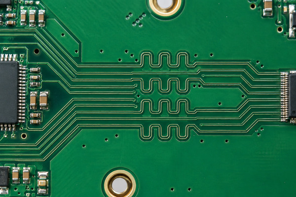
Serpentine routing adds length through controlled bends. Use it where a route falls short of its target, while preserving clearance and a continuous reference plane.
First, complete the main path and identify the remaining mismatch. Next, select a suitable tuning area and add the required length. Finally, check the resulting delay or length and review the surrounding geometry.
The main tuning checks are:
- Segment spacing: Limit unwanted coupling between adjacent sections.
- Added length: Add only the compensation required by the constraint.
- Nearby clearance: Keep tuning away from unrelated signals and crowded breakouts.
- Reference plane: Avoid crossing gaps or plane boundaries.
- Differential geometry: Preserve the intended pair relationship during adjustment.
Closely packed serpentine sections can couple to each other, changing their electrical behavior. Added geometric length does not always produce the expected delay increase. Select spacing and tuning geometry from the stackup and interface guidance rather than applying a universal 3W or 5W rule.
How Do You Verify PCB Trace Length Matching Before Manufacturing?
Verify PCB trace length matching by checking the configured rules, final routing reports, and physical geometry. Confirm whether the software evaluates length or delay and whether package and via contributions match the analysis assumptions.
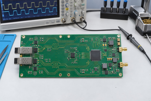
The release review should cover:
- Constraint scope: Correct nets, pairs, groups, references, and endpoints.
- Rule results: Matching limits, maximum length, and unresolved exceptions.
- Physical routing: Transitions, reference continuity, and serpentine geometry.
- Timing margin: Final path relationships against device requirements.
- Channel behavior: Signal integrity analysis where the interface warrants it.
- Revision consistency: Matching stackup and layout versions across analysis and fabrication files.
A CAD rule pass confirms compliance with the configured constraints. DFM checks manufacturing feasibility. Neither alone proves that the complete interface meets its timing requirements.
Preserve the approved material system, dielectric construction, and impedance targets during fabrication. Impedance testing verifies its specified characteristics; it does not independently certify length matching or interface timing.
FAQs About PCB Trace Length Matching
Q1: Can swapping data pins make length matching easier?
A1: Pin swapping can simplify routing when the device permits it, provided the schematic, pin mapping, and required configuration are updated consistently.
Q2: Can temperature changes affect trace-matching performance?
A2: Temperature-dependent material and device behavior can change timing margin, so designs with tight budgets should be evaluated across their specified operating range.
Q3: Does receiver training eliminate PCB length-matching requirements?
A3: Receiver training compensates within its supported range, while the board must still satisfy the device’s routing limits.
Q4: Can test points affect an otherwise matched signal path?
A4: Test-point pads and branches can introduce loading or stubs, so matching the main routes alone does not establish acceptable channel performance.
Q5: Can firmware correct excessive routing skew?
A5: Firmware can adjust timing only where the hardware provides suitable controls and sufficient adjustment range.
Q6: Should tuning patterns be placed beneath a connector or component body?
A6: They can be placed there when electrical spacing, reference continuity, and footprint restrictions permit, with nearby pads and holes included in the review.
For PCB fabrication or assembly support, send your Gerber or ODB++ files, approved stackup, impedance requirements, quantities, and BOM where applicable to sales@bestpcbs.com. Our engineering team can review manufacturing requirements and provide technical support and quotations for prototype and volume production.