Wireless technology has transformed the way devices communicate. At the heart of this transformation are Wi-Fi modules. These small components power a wide range of applications, from home automation to industrial systems. In this blog, we’ll explore the functions of Wi-Fi modules, their uses, design considerations in PCB assembly and their differences from Bluetooth.
What is a Wi-Fi Module?
The Wi-Fi module, also known as the wireless module, belongs to the transmission layer of the Internet of Things (loT). It integrates a processor, memory, transceiver, and sometimes an antenna. A Wi-Fi module is to convert the serial port or TTL level into an embedded module that meets the Wi-Fi wireless network communication standards, with built-in wireless network protocol IEEE802.11b.g.n protocol stack and TCP/IP protocol stack.
The module handles the task of connecting a device to a wireless router, allowing it to send and receive data over the internet. If embedded a Wi-Fi module in traditional hardware devices, then we can directly use Wi-Fi to connect to the Internet. It can be said, it is an important part of wireless smart home, M2M and other IoT applications.
Types of Wi-Fi Module
According to the different functions, Wi-Fi modules can be divided into three categories:
1. General Wi-Fi modules
Such as USB or SDIO interface modules on our mobile phones, laptops and tablets. Wi-Fi protocol stack and driver are run in Android, Windows and IOS systems, which require a very powerful CPU to complete the application.
2. Router Wi-Fi module
The most typical one is our home router, its protocol and driver has powerful Flash and Ram resources chip plus Linux operating system.
3. Embedded Wi-Fi module
Such as 32-bit MCU, built-in Wi-Fi driver and protocol, interface for the general MCU interface such as UART. Suitable for all kinds of smart home or smart hardware items.
What is the Difference Between Wi-Fi and Bluetooth Modules?
While both Wi-Fi and Bluetooth modules enable wireless communication, their usage and performance differ significantly:
1. Frequency
The frequency of Wi-Fi has 2.4G and 5G bands. Wi-Fi 2.4G band has 13 channels, 2401~2423MHz. Wi-Fi 5G frequency band is divided into 5.2G band and 5.8G band, and the 5.8G frequency band is: 149, 153, 157, 161, 165; The 5.2G band must support 11ac, and the available channels are 36, 40, 44, 48, 52, 56, 60, and 64. Under normal circumstances, it is recommended to avoid 52, 56, 60, 64 channels, because they conflict with radar channels;
Bluetooth only has 2.4G band: 2.402GHz ~ 2480GHz, a typical Bluetooth has 76 channels, each channel is 1MHz. And bluetooth BLE has 40 channels, each channel 2MHz, of which 37 channels belong to the data channel, 3 channels belong to the broadcast channel;
2. Application
Wi-Fi can directly access the network, and Bluetooth needs conversion processing. Therefore, WiFi is more suitable for 1-to-many local area networking, such as home and company Internet access environment. Compared with Wi-Fi module, bluetooth is more suitable for short-range and high-stability transmission, such as smart headphones. Additionally, bluetooth mesh networking is especially suitable for smart home wireless control and other applications.
3. Transmission Distance
The transmission distance of Wi-Fi is further than that of Bluetooth, which can reach several hundred meters, while the transmission distance of Bluetooth is generally within 100 meters;
4. Transmission Rate
Wi-Fi: 54Mbps; Bluetooth: 2Mbps;
Wi-Fi is more suitable for big data transmission.
5. Speed
Wi-Fi is generally faster than Bluetooth. It can handle large file transfers or streaming content without any issues. Bluetooth is slower but works well for smaller data transfers like audio streaming or simple file sharing.
What is the Range of a Wi-Fi Module?
The coverage range of the WiFi module usually depends on the specific application scenario and environmental conditions. According to the IEEE 802.11 standard, the maximum distance that wireless devices can cover is usually 300 meters, but this depends on the environment is open or not.
In the specific environment, the coverage of the WiFi module will be affected by a variety of factors. For example, in an ideal environment of accessibility and interference, the wireless transmission distance of a wireless router is 100 meters indoors and 300 meters at outdoors. In the actual home environment, the wireless signal will be attenuated when passing through obstacles such as walls, glass, doors, and furniture, affecting the transmission distance. If an external antenna is used, the transmission distance can reach 30 ~ 50 km or even more, depending on the gain of the antenna itself.
Advantages of Wi-Fi Module
1. Wide coverage
WiFi module supports IEEE 802.11b/g/n and other standards to provide a wide range of wireless coverage, suitable for a variety of indoor and outdoor environments.
2. High-speed transmission
WiFi module supports a high data transmission rate, which can meet the requirements of high-speed data transmission, and is suitable for application scenarios with a large amount of data.
3. Compatibility and ecosystem
WiFi module supports a variety of communication protocols, such as Wi-Fi, Bluetooth, etc., has good compatibility and ecosystem, and can be integrated with a variety of devices and services.
4. Easy to install and use
WiFi modules are usually plug and play, easy to install and use, suitable for a variety of devices and system integration.
Disadvantages of a Wi-Fi Module
1. Power consumption
One downside of Wi-Fi modules is their higher power usage compared to other wireless technologies, such as Bluetooth. This can be a concern for devices running on battery power.
2. Interference
Wi-Fi operates on the same frequencies as other devices, such as microwaves and cordless phones.
3. Security
Since Wi-Fi networks are widespread, they can be vulnerable to hacking. Proper security measures, such as encryption, must be implemented to protect data.
What is a Wi-Fi Module Used For?
Wi-Fi modules have a wide range of applications across industries. Actually, it exist everywhere need networks. It can be said, it can be used in every fields. Here are some typical applications:
- Smart Homes
Wi-Fi modules power smart devices like security cameras, thermostats, and lighting systems. They connect to a home Wi-Fi network, so users to control them remotely through apps.
- Industrial Equipment
In manufacturing or logistics, Wi-Fi modules enable machines to communicate wirelessly.
- Consumer Electronics
Devices like laptops, gaming consoles, and smart TVs rely on Wi-Fi modules for wireless internet access.
- Healthcare Devices
Medical equipment, such as patient monitors or wearable devices, often use Wi-Fi modules to transmit data to a healthcare provider in real time.
- IoT Devices
The IoT relies heavily on Wi-Fi modules. Devices ranging from smart refrigerators to connected doorbells use Wi-Fi to communicate with each other and with cloud-based systems.
Wi-Fi Module Price
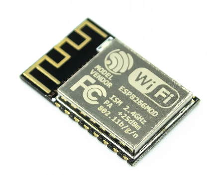
Wi-Fi modules are available at various price points, depending on their features and intended use. For instance, the ESP8266 typically costs between $2 to $5. The ESP32, with its additional capabilities, is priced slightly higher, ranging from $5 to $10. High-end industrial Wi-Fi modules can be more expensive, ranging from $20 to $50.
The price may also vary depending on factors like antenna design, supported protocols, and whether the module is designed for mass production or individual projects.
What is the Most Common Wi-Fi Module?
The ESP8266 is one of the most popular and widely used Wi-Fi modules. It is favored in many IoT applications due to its low cost, ease of use, and compact size. Another frequently used module is the ESP32, which offers additional features such as dual-core processing, built-in Bluetooth. In addition to them, there are some other common Wi-Fi module that used in the electronics.
| Wi-Fi Module | Description | Frequency Brand | Range | Price | Special Features |
| ESP8266 | Popular for IoT applications due to low cost and ease of use. | 2.4 GHz | Up to 150 feet | $2 – $5 | Compact size, low power, integrated TCP/IP protocol stack. |
| ESP32 | Offers better performance with dual-core and built-in Bluetooth. | 2.4 GHz, Bluetooth | Up to 300 feet | $5 – $10 | Dual-core processing, Bluetooth, multiple I/O options. |
| CC3200 | A Texas Instruments Wi-Fi module designed for IoT and smart products. | 2.4 GHz | Up to 200 feet | $8 – $15 | Built-in ARM Cortex-M4 processor, low power, encryption features. |
| RN171 | A high-performance Wi-Fi module from Microchip. | 2.4 GHz | Up to 330 feet | $20 – $30 | Embedded TCP/IP stack, simple serial interface. |
| ATWINC1500 | A low-power module designed for IoT and wearable devices. | 2.4 GHz | Up to 200 feet | $7 – $15 | Ultra-low power, integrated network stack, supports power-saving modes. |
| WizFi210 | A stable Wi-Fi module designed for industrial applications. | 2.4 GHz | Up to 300 feet | $10 – $25 | Low power, fast boot-up, secure connection. |
| Roving Networks RN131 | Suitable for long-range industrial and commercial applications. | 2.4 GHz | Up to 400 feet | $25 – $40 | High-performance, robust design, supports SSL encryption. |
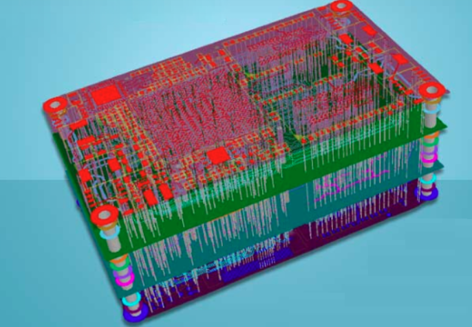
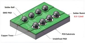
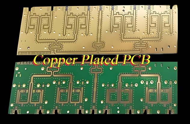
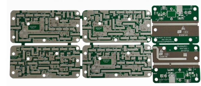
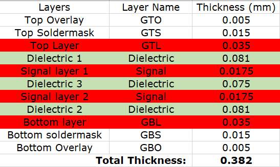
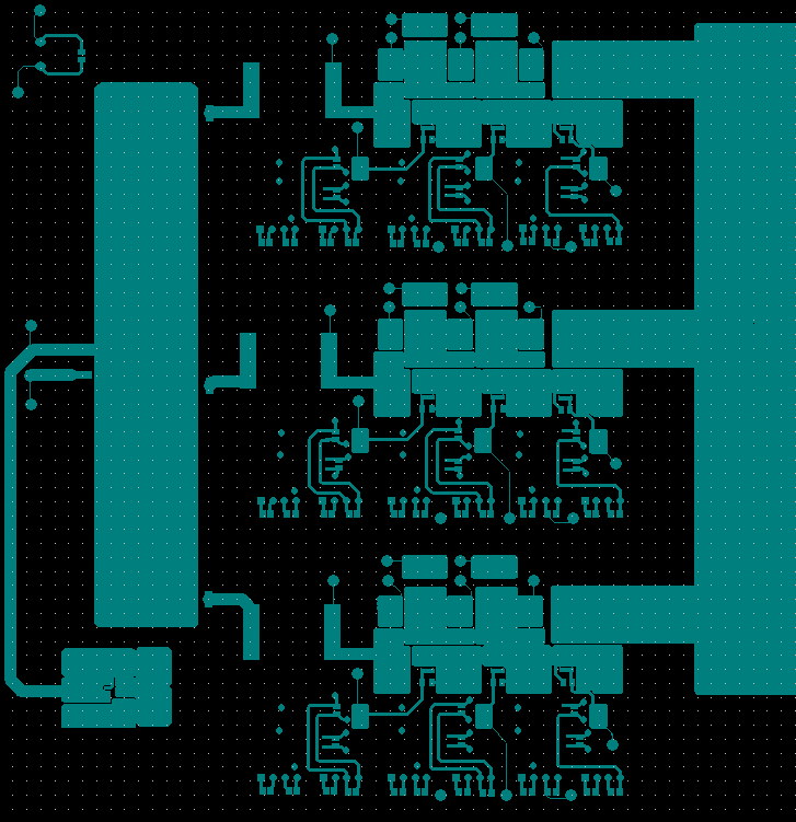
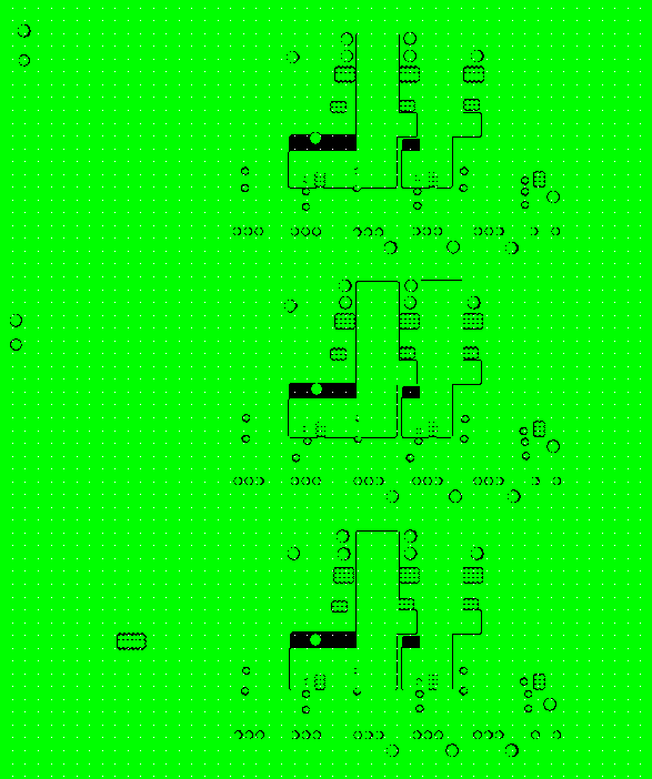
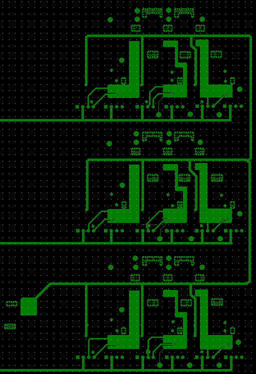
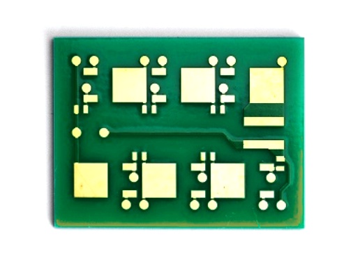
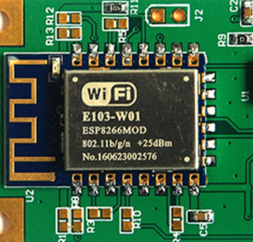
Considerations in PCBA Design with a Wi-Fi Module
When integrating a Wi-Fi module into PCBA design, several factors need to be considered to ensure optimal performance:
- Antenna Design and Placement
A key factor in wireless performance is the placement of the antenna. Ensuring there are no obstructions near the antenna can significantly improve signal strength. The module should be positioned to minimize interference from nearby components.
- Power Supply
Wi-Fi modules require a stable and sufficient power supply to function effectively. Voltage fluctuations or insufficient power can result in poor connectivity or even module failure.
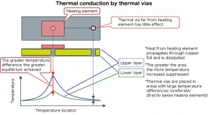
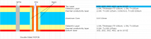
- Thermal Management
Wi-Fi modules can generate heat, especially during heavy use. Proper heat dissipation methods, such as using heat sinks or thermal vias, should be incorporated into the PCBA design to maintain optimal performance.
- EMI and EMC Compliance
Wireless communication devices must adhere to electromagnetic interference (EMI) and electromagnetic compatibility (EMC) standards. Proper shielding and circuit design can help reduce interference and improve reliability.
- Firmware Integration
Many Wi-Fi modules come with firmware that handles wireless communication tasks.
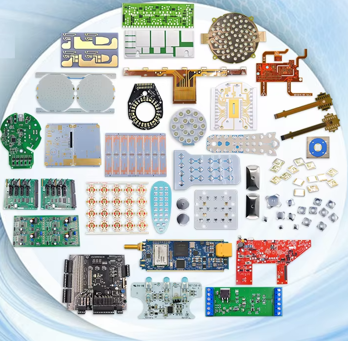
One-Stop Box-Build Assembly for Wireless Communication Devices
For companies looking to develop wireless communication devices, EBest Circuit (Best Technology) is your go-to choice. We offer one-stop PCBA and box-build service that can handle everything from component sourcing and PCBA design to final product assembly. By partnering with us, you can reduce much development time, and get a high quality, fast delivery, low cost PCBA with Wi-Fi modules.
With over 18 years of experience in printed circuit boards and as one of the leading PCB manufacturers, we support over 2,000 customers in different industrial areas worldwide. You can count on a PCB board manufacturer like us to meet your one-stop electronics manufacturing demands. We have an experienced engineer, production and quality team to fully understand the unique requirements of your industry, such as the particular acceptance criteria in medical, automotive, communication and aerospace industries. Contact us right now to get your PCB quotation!