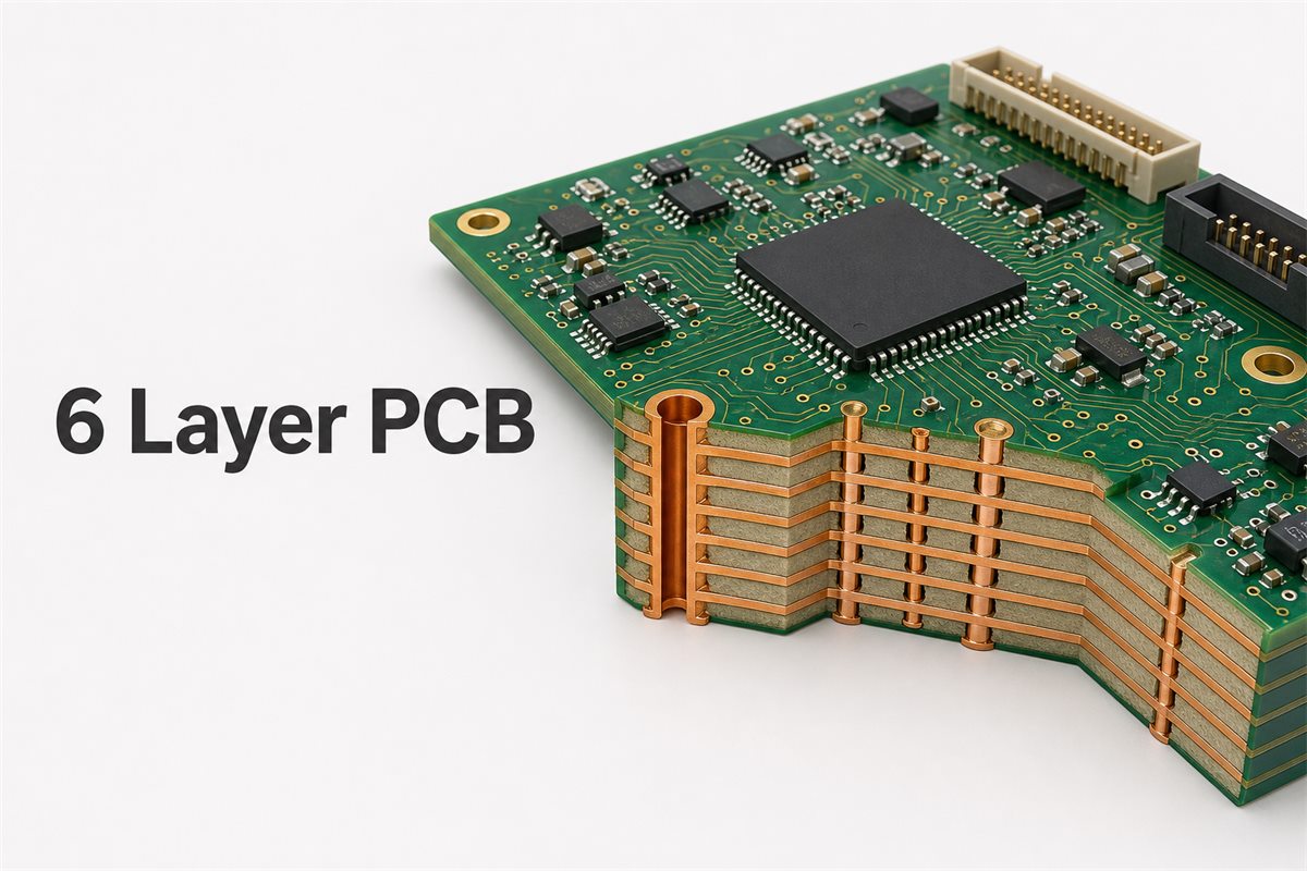
A 6 layer PCB uses 6 copper layers to create more routing space, stronger reference-plane coverage, and better control of power and signal return paths than a typical four-layer board. It is often a practical middle ground when a design has outgrown four layers but does not yet need the routing density or additional plane pairs of an eight-layer construction.
The layer count alone does not guarantee good performance. A successful board depends on how signals, ground, and power are assigned; how close each critical trace is to a continuous reference plane; and whether the fabricator can build the proposed geometry reliably. This guide turns those decisions into a design-to-release workflow.
What Is a 6 Layer PCB?
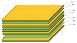
A 6-layer board contains 6 patterned copper layers separated by dielectric material and laminated into one rigid structure. The outer copper layers normally carry components and routing. The internal layers may be assigned to signals, ground, power, or a combination of plane regions and routed conductors.
There is no universal rule that says a 6-layer board must contain a fixed number of signal layers and planes. The correct allocation depends on interface speed, component density, power distribution, EMC goals, mechanical thickness, and cost. What matters is that critical signals see a continuous return path and that power distribution remains predictable.
| Layer count | Typical fit | Main design trade-off |
|---|---|---|
| 4 layers | Moderate density, simpler interfaces | Limited routing and plane flexibility |
| 6 layers | Higher net count, mixed interfaces, compact layouts | Requires disciplined layer assignment |
| 8 layers | More plane pairs, more signal separation, dense BGA routing | Higher fabrication cost and added stackup complexity |
When Should You Move From 4 Layers to 6 Layers?
Move to 6 layers when the 4-layer layout forces compromises that create more risk than the extra layer cost. Common signs include crowded outer layers, frequent reference-plane changes, split return paths, excessive via transitions, difficult BGA escape routing, and power distribution that competes with signal routing.
- Routing density: Components fit, but critical nets cannot be routed cleanly without long detours.
- Reference continuity: High-speed traces would cross plane gaps or change reference layers without a nearby return path.
- Mixed-signal organization: Analog, digital, power, and sensitive measurement sections need clearer physical and electrical separation.
- Power delivery: Multiple rails need lower-inductance distribution than narrow surface traces can provide.
- EMI control: More adjacent ground-reference coverage can reduce loop area when the layout and stackup are coordinated.
If routing is already easy and interfaces are slow, adding layers may not improve the product. A good layer-count decision starts with the schematic, placement, expected edge rates, current demand, connector locations, and mechanical constraints—not with a preferred number in isolation.
6 Layer PCB Stackup: Start With Return Paths
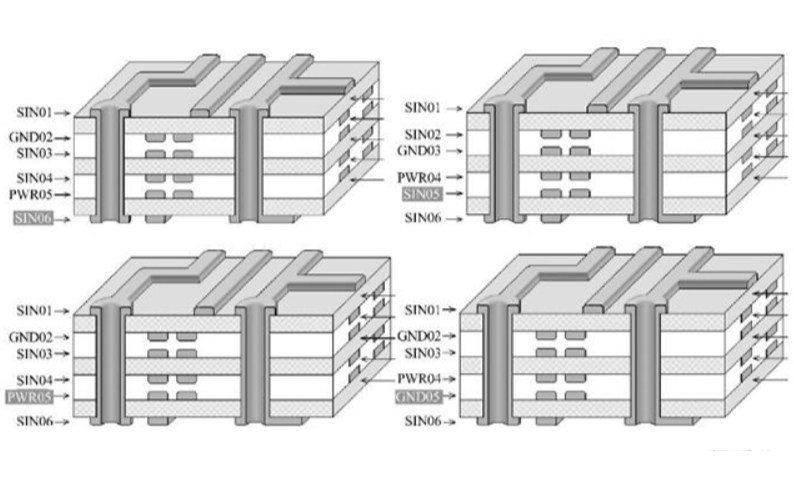
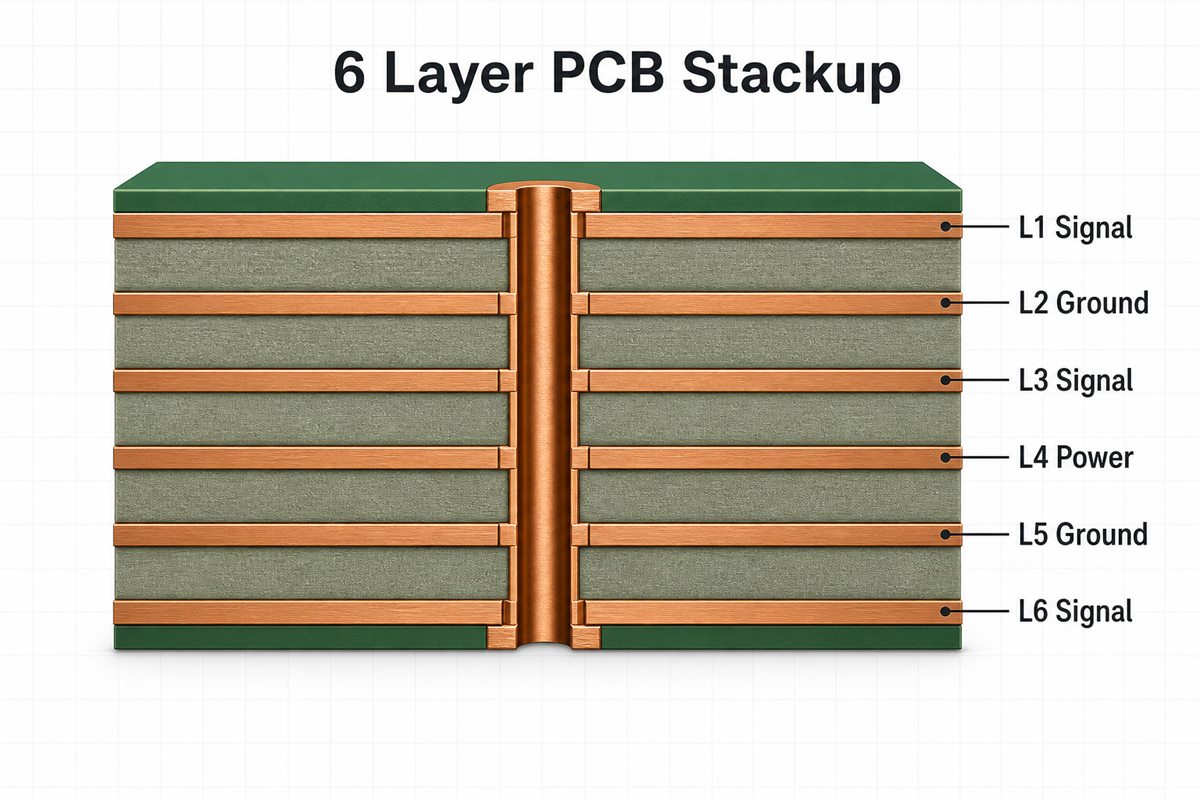
A useful 6 layer pcb stackup places important signal layers next to continuous reference planes. One common conceptual arrangement is:
- L1: components and critical signals
- L2: solid ground plane
- L3: signal routing or power regions
- L4: power distribution or signal routing
- L5: solid ground plane
- L6: components and signals
This is a planning example, not a fabrication prescription. Material type, copper weight, dielectric thickness, finished board thickness, impedance targets, and layer symmetry must be agreed with the PCB manufacturer. For a deeper treatment of alternative arrangements, see the existing BestPCBs guide to 6 layer PCB stackup, thickness, and impedance control.
Avoid Broken Return Paths
A critical trace should not cross a split in its reference plane. At high edge rates, return current follows the path of lowest impedance near the trace. A plane gap forces the return current to detour, increasing loop area and the chance of radiation or coupling. If a signal must change reference planes, place an appropriate stitching path near the transition and review the current loop, not only the signal trace.
Keep the Stackup Symmetrical
Balanced copper and dielectric construction helps the fabricator control bow and twist. Large copper-density differences can also affect etching and lamination. Add copper balancing only under manufacturer guidance; do not fill areas blindly where the added copper could disturb impedance, isolation, or antenna behavior.
6 Layer PCB Thickness and Dielectric Planning
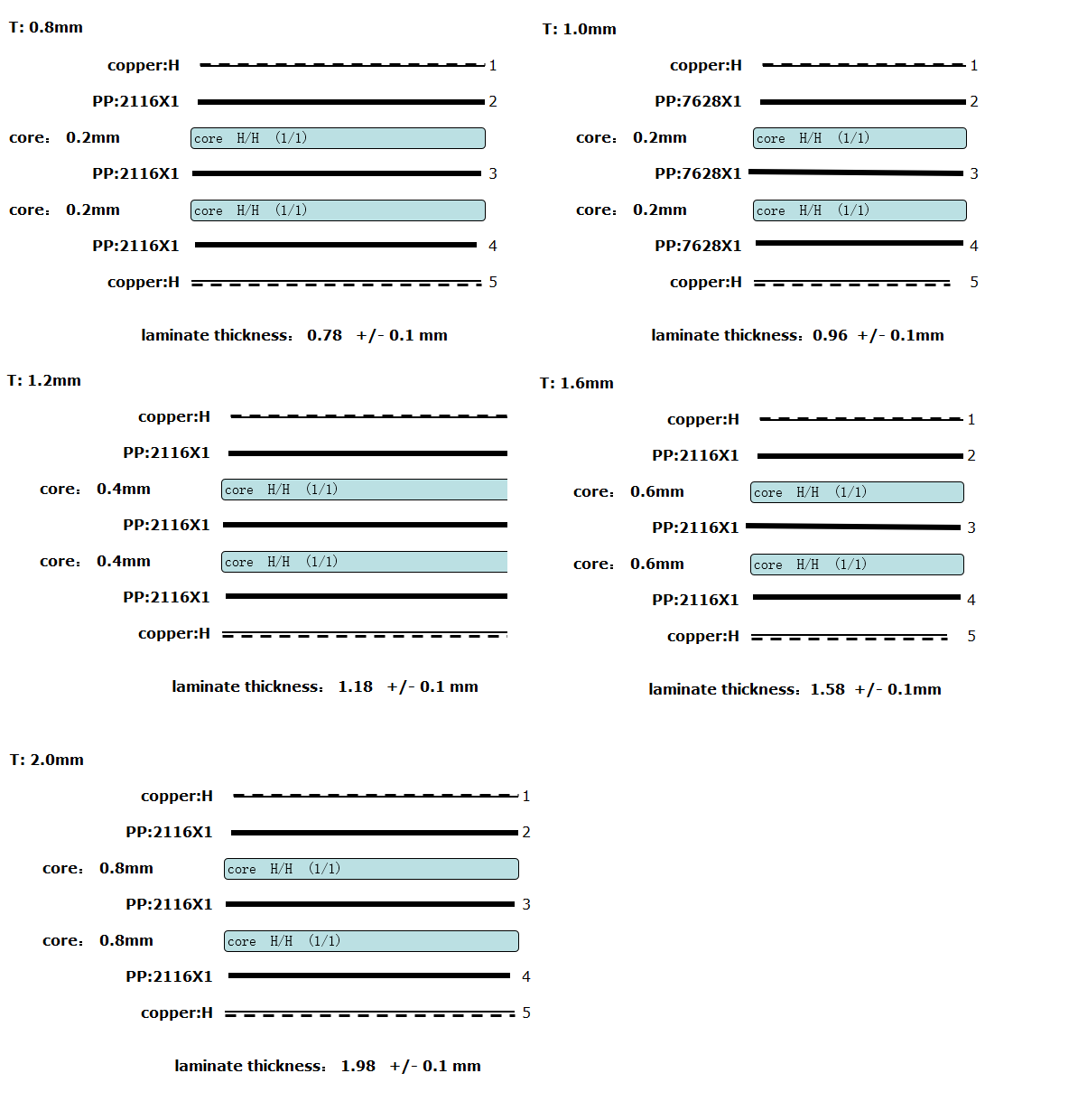
6 layer pcb thickness is not automatically 1.6 mm. A finished thickness near 1.6 mm is common for many assemblies, but thinner and thicker boards are possible. The correct value depends on connector requirements, enclosure fit, stiffness, controlled-impedance geometry, copper weight, and the manufacturer’s qualified material constructions.
Do not select the total thickness first and squeeze every dielectric until the number fits. Start with electrical and mechanical constraints. Controlled-impedance traces may need specific reference-plane spacing, while press-fit connectors or edge fingers may impose separate thickness tolerances. Ask the fabricator for a production-ready stackup before finalizing trace widths and spacing.
6 Layer PCB Design Guidelines for Routing
Good 6 layer pcb design treats placement, return paths, power integrity, and manufacturability as one problem. The following sequence reduces late changes.
1. Place by Signal Flow and Return Flow
Place connectors, processors, memory, converters, sensors, and protection parts so that critical paths remain short and direct. Keep decoupling capacitors close to the power pins they support, with short connections to power and ground. Leave enough routing channels around dense packages before locking mechanical details.
2. Route Critical Interfaces First
Route clocks, differential pairs, RF paths, fast serial buses, and sensitive analog nets before general-purpose signals. Maintain the geometry used by the impedance model. Avoid unnecessary layer changes, stubs, sharp discontinuities, and reference-plane gaps. Length matching should follow the interface requirement; matching every unrelated trace only consumes space.
3. Plan Via Transitions
Every via adds inductance and creates a discontinuity. Through vias are economical and suitable for many 6-layer designs, but they can block routing channels under fine-pitch BGAs. Blind vias or via-in-pad may help dense escape routing, yet they add process steps and cost. Use advanced via structures only where placement and fan-out analysis show a clear need.
4. Protect Sensitive Circuits
Keep switching nodes compact and away from high-impedance analog inputs, antennas, clocks, and board edges. Do not split ground simply to label analog and digital regions. First control placement and current paths; then connect circuits so return currents do not share harmful routes.
5. Define Controlled Impedance With the Fabricator
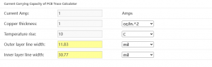
Impedance depends on trace geometry, copper thickness, dielectric thickness, dielectric properties, solder mask, and the chosen reference plane. A calculator is useful for initial routing, but fabrication values should come from the real material set. BestPCBs can review requirements for an impedance control PCB before production data is frozen.
4 Layer vs 6 Layer PCB
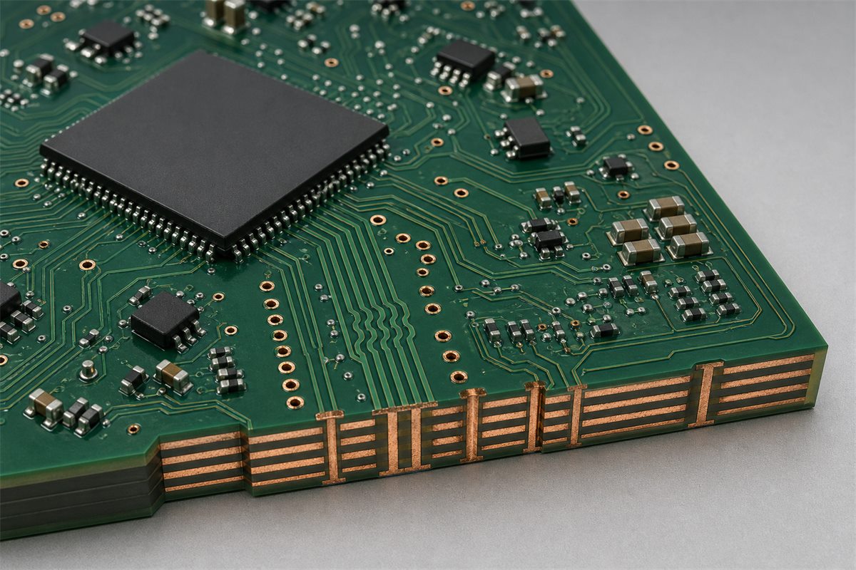
The practical 4 layer vs 6 layer pcb decision is not only a price comparison. Four layers may be the better choice for a low-density product with simple power needs. 6 layers become valuable when they eliminate routing congestion, add continuous reference coverage, support a dedicated power structure, or reduce redesign risk.
A 6-layer board may also reduce area enough to offset part of the layer premium, but that outcome depends on component placement, technology choices, and quantity. Compare complete manufactured designs rather than layer count alone.
6 Layer vs 8 Layer PCB
In a 6 layer vs 8 layer pcb comparison, eight layers provide more freedom to separate signal groups, add plane pairs, or support dense BGA escape routing. 6 layers are often sufficient when two solid reference planes and carefully assigned signal or power layers satisfy the electrical plan.
Choose eight layers when the six-layer arrangement would force high-speed signals onto poorly referenced layers, require many plane splits, or leave too little room for power and routing. Choose six when the design closes cleanly without those compromises.
DFM Checks Before Releasing a 6 Layer PCB
Design-rule checking is necessary, but it does not replace fabrication review. Before release, confirm that the stackup, drill plan, copper features, solder-mask openings, controlled-impedance requirements, and board outline match a qualified manufacturing process.
- Obtain the manufacturer’s proposed stackup and material construction.
- Confirm minimum trace, spacing, annular ring, drill, and copper-to-edge rules.
- Review via aspect ratio, finished hole sizes, and any blind or buried via sequence.
- Identify impedance-controlled nets, targets, reference layers, and tolerances.
- Check copper balance, plane clearances, thermal reliefs, and isolated copper.
- Verify solder-mask dams, paste apertures, fiducials, tooling, and panel needs.
- Run netlist comparison and provide an IPC-356 netlist when available.
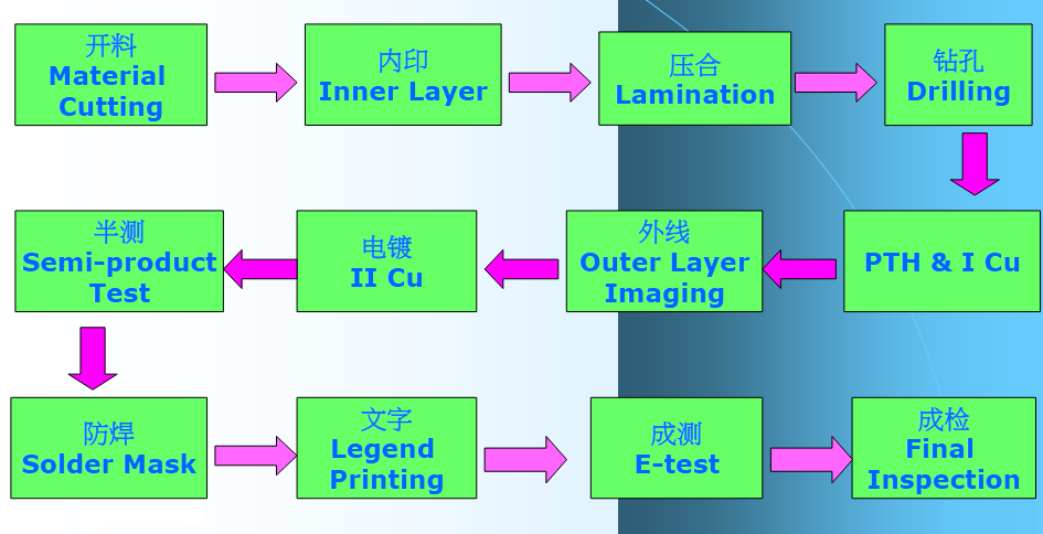
The broader multilayer PCB manufacturing guide explains how lamination, drilling, plating, imaging, and testing interact. For factory-specific limits, use the current BestPCBs manufacturing capability information and request a DFM review.

What Drives 6 Layer PCB Cost?
6 layer pcb cost is influenced by much more than the two extra copper layers. Board area, panel utilization, material, copper weight, finished thickness, feature size, hole density, via technology, impedance control, surface finish, testing, quantity, and delivery schedule all affect the quote.
The most effective cost control happens before routing is complete. Use standard material constructions where they meet the electrical need, avoid unnecessarily tight tolerances, keep advanced vias limited to the areas that require them, and design the outline for reasonable panel utilization. The BestPCBs custom PCB cost guide provides a broader checklist for comparing quotations.
Files to Send for a Manufacturing Review
A complete release package reduces assumptions and quote revisions. Include:
- Gerber X2 or ODB++ fabrication data
- NC drill files with plated and non-plated holes identified
- A fabrication drawing with dimensions, tolerances, material, finish, copper weight, and notes
- A layer-stack drawing showing each copper and dielectric layer
- Controlled-impedance net groups, targets, reference layers, and tolerances
- IPC-356 netlist when available
- Assembly files when PCBA is required: BOM, centroid/pick-and-place, assembly drawings, and special process notes
For a new 6 layer PCB design, ask for stackup confirmation before final impedance routing. That single review can prevent trace-width changes, plane reassignment, or connector-thickness problems after the layout is complete.
6 Layer PCB FAQ
How many copper layers does a 6 layer PCB have?
It has six patterned copper layers. The number of signal, ground, and power layers depends on the design’s electrical and routing needs.
How thick is a 6 layer PCB?
There is no single mandatory thickness. About 1.6 mm is common, but thinner or thicker constructions are available when materials, impedance geometry, connectors, stiffness, and manufacturing capability support them.
What is a typical 6 layer PCB stackup?
A common concept uses signal layers on the outside, solid ground planes near the outside, and two central layers for signal and power. The exact order and dielectric spacing must be selected for the application and confirmed by the fabricator.
Is 6 layer PCB good for high-speed signals?
It can be. Six layers can provide continuous reference planes and controlled-impedance routing, but performance still depends on placement, stackup geometry, routing, return paths, vias, and power integrity.
When is a 4-layer board enough?
Four layers may be enough when routing density is moderate, interfaces are not demanding, and solid reference planes can be preserved without crowding power and signal routes.
When should I choose 8 layers instead?
Choose eight layers when six cannot provide enough well-referenced routing channels, plane pairs, signal separation, or BGA escape capacity without unacceptable compromises.
Does a 6 layer PCB require blind vias?
No. Many six-layer boards use only through vias. Blind vias or via-in-pad are selected when component pitch, routing density, or electrical constraints justify the additional process complexity.
Can every signal layer use controlled impedance?
Potentially, but only when its reference plane and dielectric geometry are defined. Specify impedance only for nets that need it and identify the correct routing and reference layers.
Build the Stackup Around the Real Design
A reliable six-layer board begins with a clear reason for using six layers. Assign reference planes first, reserve routing based on real net density, define power paths, and let the fabricator tune the dielectric and copper construction before critical geometry is frozen.
If you are preparing a 6 layer PCB for quotation, send the stackup concept, Gerbers or ODB++, drill data, impedance requirements, board thickness, copper weight, material preference, surface finish, quantity, and delivery target. BestPCBs can then review manufacturability and identify any stackup or routing changes before production.