What is 1st Article Inspection For?
First Article Inspection (FAI) refers to the inspection of the first or several products produced at the beginning of production (such as every day, every shift or the beginning of each production batch) to confirm whether the production conditions (such as equipment, process, materials, environment, etc.) meet the technical and quality requirements. This is a preventive quality control measure designed to prevent batch defects by early detection of possible problems in the production process.
The first inspection usually includes the following steps:
1. Preparation stage: clear inspection standards, inspection methods, inspection tools and equipment, and prepare relevant inspection records and forms.
2. Production preparation: Check whether the production equipment is in good condition, whether the process parameters are set correctly, and whether the raw materials or parts meet the requirements.
3. Production of the first piece: Start production according to the production plan, and make the first piece or the first few products as the first piece.
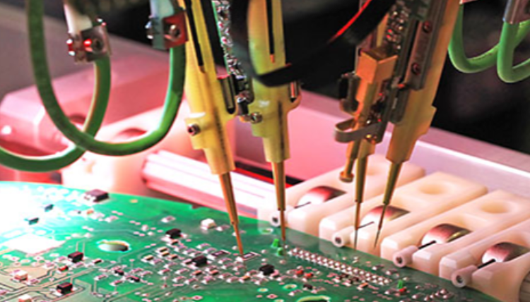
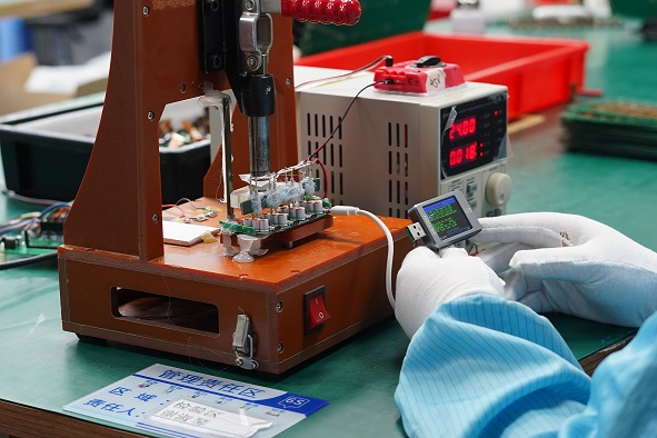
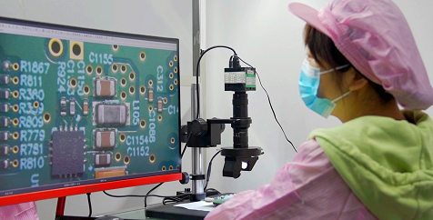
4. First inspection: Detailed inspection of the first product, including inspection of appearance, size, performance, function, etc., to ensure that the product meets the design requirements and quality standards.
5. Result judgment: According to the inspection results, determine whether the first piece is qualified. If qualified, mass production can continue; If it is not qualified, it is necessary to analyze the cause, adjust the production conditions, and re-make the first part for inspection until it is qualified.
6. Record and feedback: Record the results of the first inspection, and feedback the results to relevant departments and personnel in order to take timely measures to solve the problem.
Why Need to Perform a FAI?
◆ The first inspection in the production process is mainly to prevent the product from a batch of out-of-quality, repair, scrap. It is a means to control the product production process in advance, is an important method of product process quality control. It is an effective and essential method for enterprises to ensure product quality and improve economic efficiency.
◆ The first inspection is to find the factors affecting product quality in the production process as early as possible to prevent bad batch or scrap.
◆ The first piece can be entered into formal production after passing the inspection, mainly to prevent the occurrence of batch unqualified products.
◆ Long-term practical experience has proved that the first inspection system is an effective measure to detect problems as early as possible and prevent products from being scrapped in batches. Through the first piece inspection, it can be found that systematic causes such as severe wear of the fixture or installation positioning errors, poor accuracy of the measuring instrument, incorrect reading of the drawing, feeding or formulation errors exist, so that corrective or improvement measures can be taken to prevent the occurrence of batch nonconforming products.
What Happens if a Component Passes or Fails the FAI?
If a component passes the FAI, full-scale production can proceed to next stage. Because knowing that the process yields parts that match design criteria. Meanwhile, it builds confidence and reduces the likelihood of future issues.
If a component fails, corrective action is necessary. This means process, parameters, or used tools, materials are not suitable or with poor quality. After modifications, a new FAI may be needed to verify the adjustments work as expected.
When Should a First Article Inspection Occur?
Knowing the right time for a 1st article inspection is crucial to avoid production issues and ensure highest quality. But when exactly should this process take place? Let me tell you:
- Initial Production Run
Picture this – you’re ready to kick off a new product line or start manufacturing a brand-new part. This is the perfect time for an FAI. Performing it at this stage helps catch any potential problems right from the start. It’s like giving your process a test drive before you commit to full-scale production.
- Process Changes
Changes are inevitable in manufacturing. Maybe there’s an upgrade to your equipment or you’re switching up the method used to produce parts. Any significant change to the process means it’s time for a new FAI. Why? Because even small adjustments can lead to unexpected differences in the final product.
- Supplier Changes
If you decide to switch to a different supplier for critical components, you shouldn’t skip an FAI. Even if the new supplier promises the same specifications, differences in materials or production methods can impact the final product. An FAI here ensures that what you’re getting from the new supplier matches your quality expectations.
- Design Modifications
Tweaking a design might seem minor, but it can change everything from part fit to performance. Any time there’s an update or redesign, running an FAI confirms that the modified product still aligns with the original quality standards.
What is the Difference Between PPAP and First Article Inspection?
You might hear the terms PPAP (Production Part Approval Process) and FAI thrown around in manufacturing discussions. While they share a goal of ensuring quality, they are different in their approach, scope, and where they are commonly used.
1. Industries and Common Use
FAI is used across various industries, and it especially popular in fields like aerospace and defense. It’s typically a requirement when introducing a new part or process. PPAP, on the other hand, is most commonly linked to the automotive industry. It’s a standard method required by major automotive manufacturers to ensure that their suppliers can consistently meet production quality standards.
2. Range and Detail
FAI is about confirming that one specific piece meets all the design and specification requirements. The process involves checking the dimensions, materials, and other key aspects to ensure everything matches up before moving forward with full-scale production.
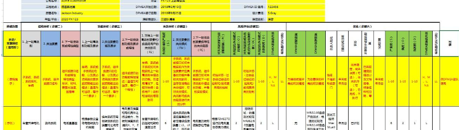
PPAP, however, takes a broader approach. Instead of just focusing on one component, PPAP is like an in-depth audit of the entire production process. It includes elements like process flow diagrams, control plans, and even failure mode and effects analysis (FMEA). PPAP doesn’t just ask, “Does this part meet the specs?” but goes further to check if the entire production line can consistently produce parts that meet quality requirements over time. A PPAP file like as below:
3. Level of Documentation
FAI has its documentation, but it’s more straightforward. You get a detailed report of the inspected part, including dimensions and results from any tests performed. With PPAP, the documentation is more comprehensive and multi-layered. It often involves around 18 sheets, including a sample production run, process validation reports, and customer-specific requirements.
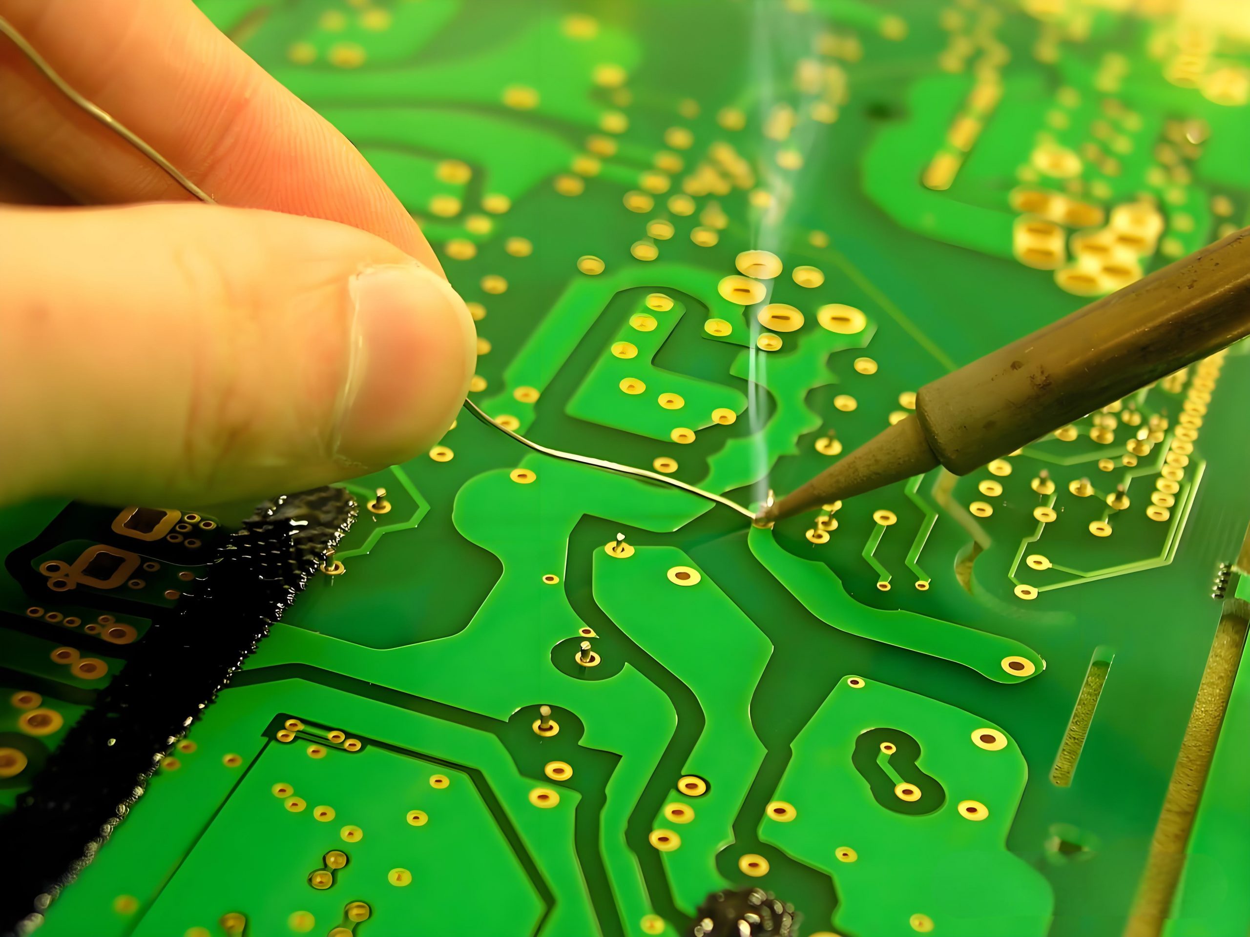
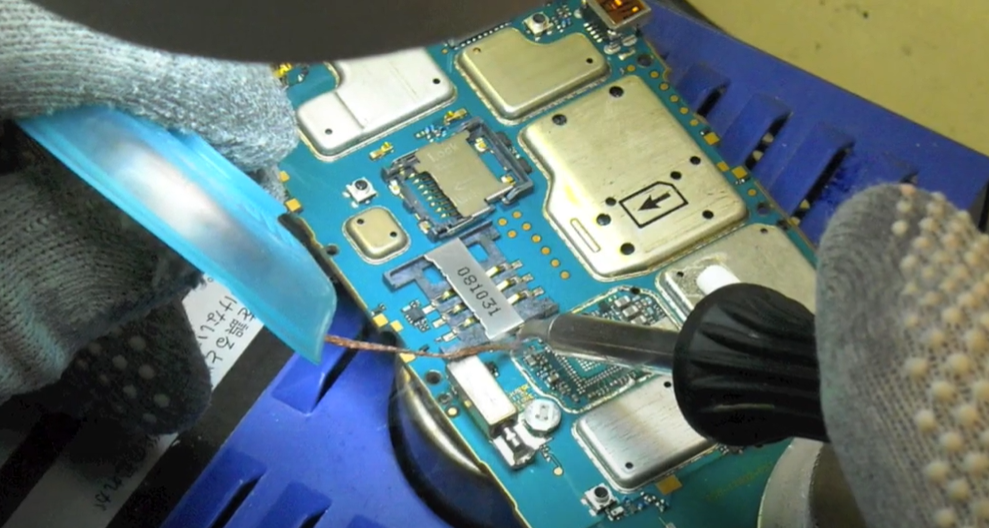
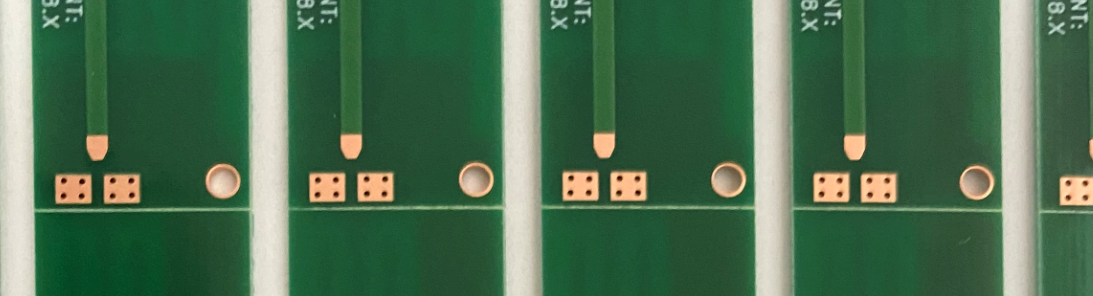
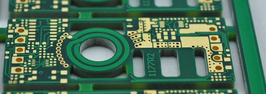
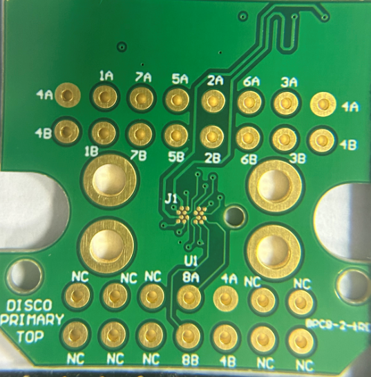
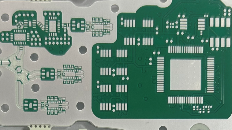
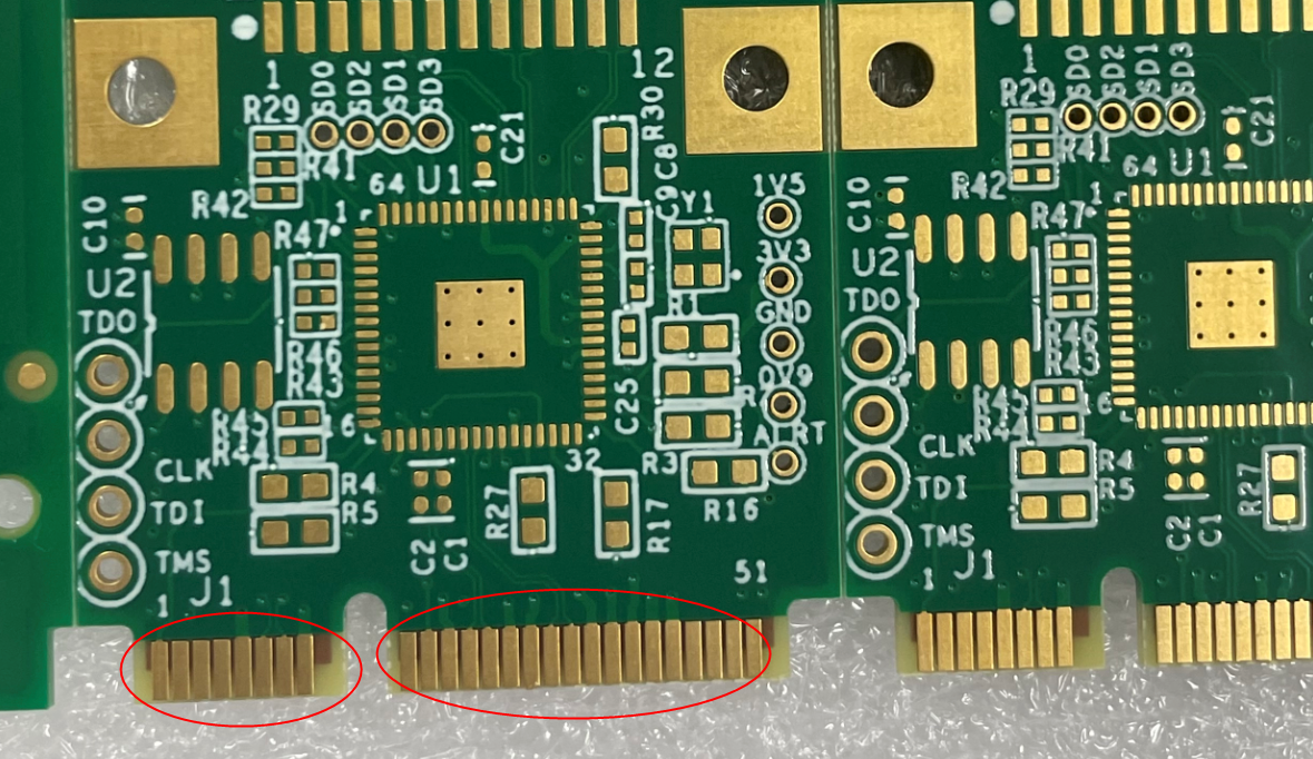
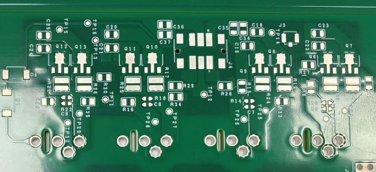
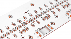
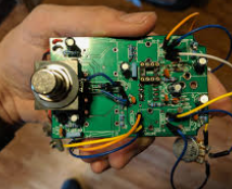
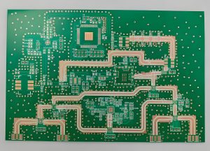
First Article Inspection in EBest Circuit (Best Technology)
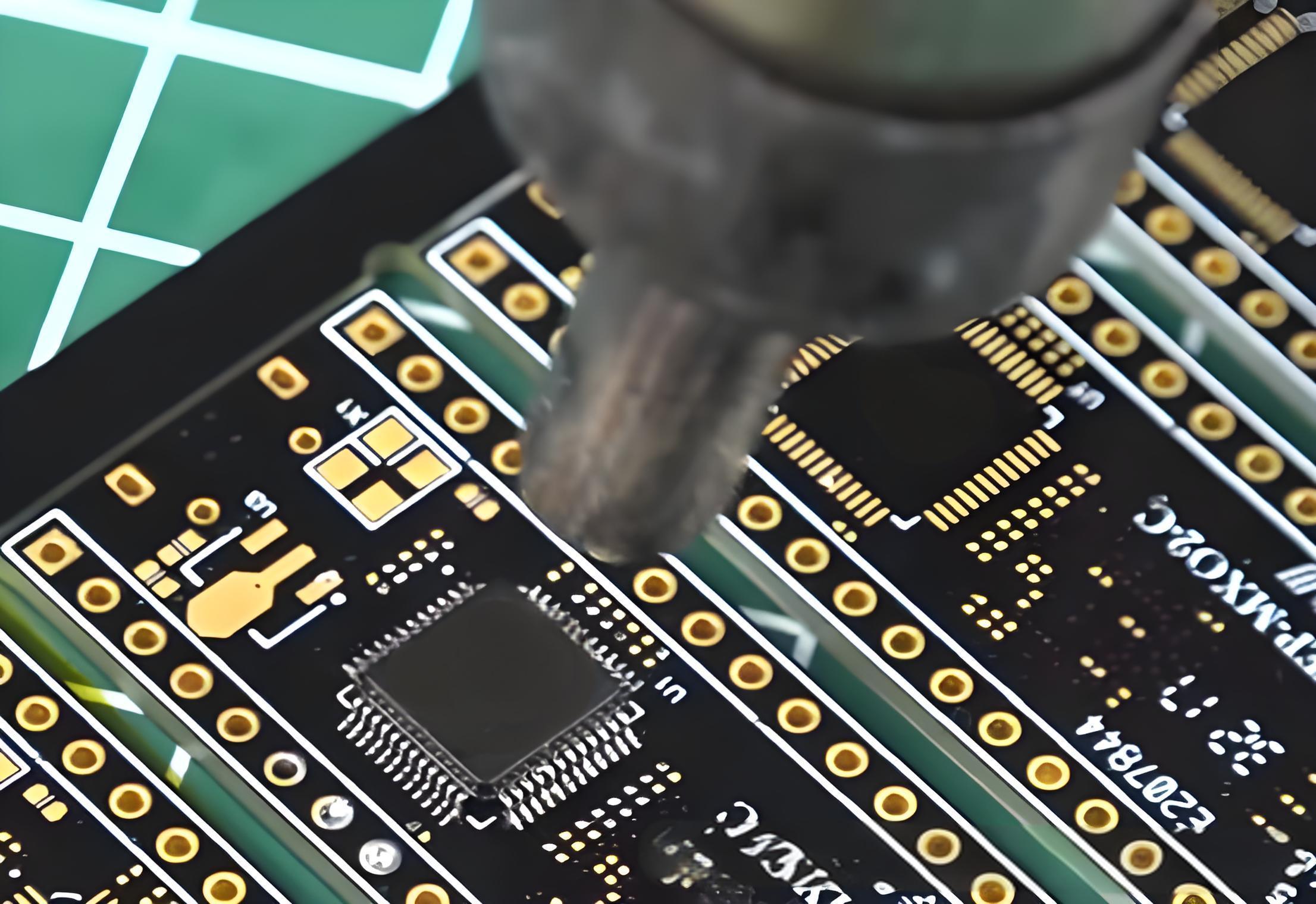
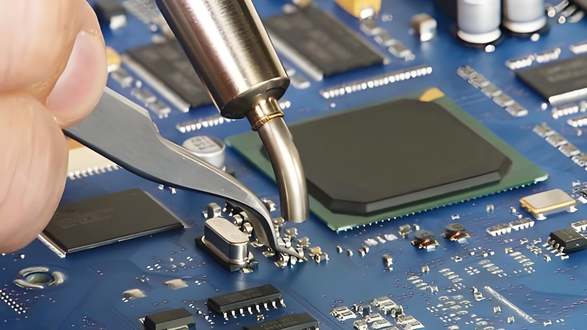
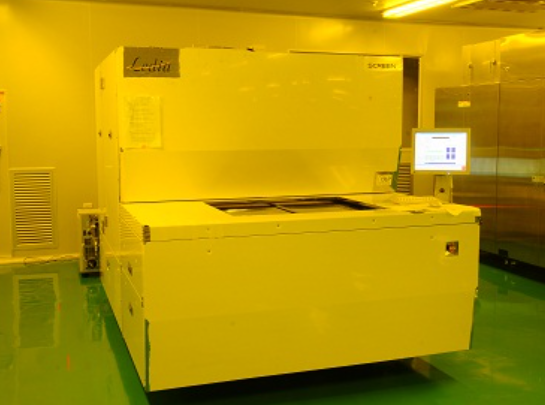
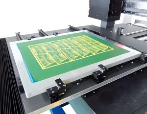
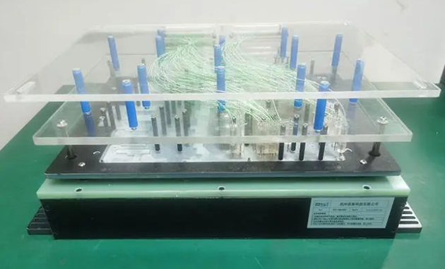
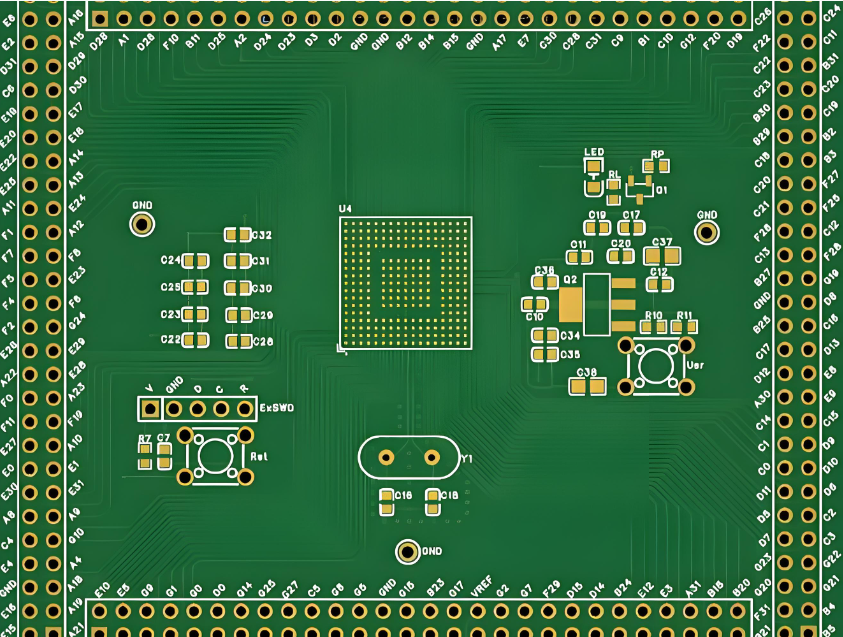
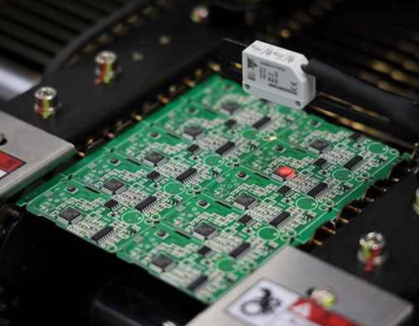
At EBest Circuit (Best Technology), we believe that FAI is more than a formality—it’s a guarantee of reliability and quality. So, we pay more attention to the first article inspection, from every step, every operator, every report. We have a 1st article inspection tester in our factory, for each prototype, we can finish the FAI inspection quickly and effectively.
As an advanced PCB and PCBA manufacturer, we have more than 18 years experiences in this industry. We have served over 5000 customers with 98% satisfied comments. All of them are amazed with our one-stop service and quick delivery.