What is a Dual Inline Package (DIP)?
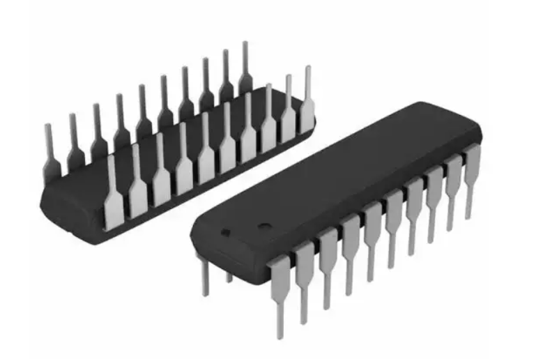
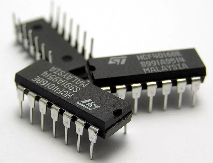
A Dual Inline Package (DIP) is a type of packaging for electronic components, especially integrated circuits (ICs). It features a rectangular body with two parallel rows of pins extending downward. These pins allow the component to be mounted onto a circuit board, typically by soldering or inserting them into a socket.
DIPs are commonly used in both analog and digital circuits, they are widely recognized in the electronics industry due to their straightforward design and ease of use. Unlike more modern surface-mount devices (SMDs), which require specialized equipment, DIPs can be inserted and soldered manually. This made DIPs a preferred choice for hobbyists, engineers, and educational institutions.
The DIP format supports a broad range of electronic devices, from simple logic gates to complex microcontrollers, and remains relevant in prototyping, testing, and certain industrial applications.
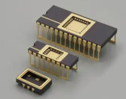
Structure of DIP package
There are three types of structure of DIP package, they are –
- Multi-layer ceramic dual-inline DIP
- Single-layer ceramic dual-inline DIP
- Lead frame type DIP (including glass ceramic sealing type, plastic encapsulation structure type, ceramic low-melting glass packaging type).
Features of Dual Inline Package
- Easy to weld and repair
The pin design of the DIP package makes the welding process simpler, and engineers can easily insert the integrated circuit into the PCB hole and weld it. This structure also makes servicing easier, as components that fail or need to be replaced can be removed and replaced with relative ease.
- Good heat dissipation
Because DIP packages typically have a larger shell surface area, they have better thermal performance than some smaller package forms. This is essential for the stability and reliability of integrated circuits under high load conditions, and good heat dissipation can extend the service life of components.
- Strong Compatibility
The DIP package has high compatibility and can be used with many types of sockets, strips and connectors. This means that there is more flexibility to choose DIP-packaged components in different circuit designs without worrying about compatibility issues.
- Easy to automate production
Because the pin arrangement of the DIP package is regular and easy to identify, it is suitable for automated production. Robots or devices on the production line can easily identify and process DIP-packaged components, increasing production efficiency and reducing production costs.
- High stability and reliability
The design of the DIP package makes the connection between the component and the PCB stronger, reducing the risk of poor connection due to vibration or temperature changes. This makes DIP packaging widely used in some application scenarios that require high stability and reliability, such as medical devices, aerospace and other fields.
- Easy identification and classification
The pins on the DIP package are usually arranged in standard spacing, and the pin numbers are clearly visible. This allows engineers to easily identify the functions of different pins, facilitating proper installation and commissioning of components. At the same time, the standardized pin arrangement is also conducive to component classification and inventory management.
History of DIP Packages
The history of DIP packaging dates back to the 1960s, a time when the electronics industry was rapidly evolving. Before the introduction of DIPs, electronic components were often housed in bulky, cumbersome packages that made assembly difficult and limited their use in compact devices.
Texas Instruments is credited with pioneering the development of the DIP format. The company introduced the first DIP in 1964, offering a practical solution for mounting integrated circuits. The new design quickly gained popularity due to its simplicity and versatility.
By the 1970s, DIPs had become the industry standard for integrated circuits, appearing in everything from consumer electronics to industrial control systems. They played a crucial role in the development of personal computers, with early models like the Apple II and IBM PC featuring numerous DIP-packaged chips on their motherboards.
Although surface-mount technology (SMT) has largely replaced DIPs in modern high-volume production, their impact on the electronics industry is undeniable. DIPs remain a symbol of the early days of the digital revolution and continue to be used in specific applications where their unique advantages are still relevant.
Pin Numbers and Spacing
One of the defining characteristics of a dual inline package is its pin configuration. DIPs are available in a wide range of pin counts, allowing them to accommodate different types of integrated circuits and other components.
Pin Count
The number of pins in a DIP typically ranges from 4 to 64. Some of the most common configurations include:
- 8-pin DIP (used for small ICs like operational amplifiers)
- 14-pin DIP (popular for logic gates and small microcontrollers)
- 16-pin DIP (frequently used for dual in-line memory modules)
- 24-pin DIP (common for larger microcontrollers and memory chips)
- 40-pin DIP (used for more complex devices, such as early microprocessors)
Pin Spacing
The spacing between adjacent pins, known as the pitch, is typically 2.54 mm (0.1 inches). This standardized spacing makes DIPs compatible with a variety of sockets, breadboards, and PCB layouts.
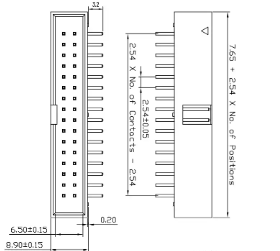
The distance between the two parallel rows of pins, referred to as the row pitch, is usually 7.62 mm (0.3 inches) for standard DIPs. This uniformity simplifies PCB design and assembly, allowing designers to use off-the-shelf components and prototyping tools.
DIP Package Dimensions
The dimensions of a dual inline package depend on the number of pins and the specific type of component it houses. However, the following are typical dimensions for standard DIPs:
Width: Common widths are 7.62 mm (0.3 inches) or 15.24 mm (0.6 inches).
Length: The length depends on the pin count, with each pin typically adding 2.54 mm to the overall length.
Height: The height is usually around 5 mm to 6 mm, providing a compact profile.
These dimensions make DIPs a practical choice for many applications, offering a balance between size and ease of handling.
What is the Function of the DIP?
DIPs are commonly used in applications where components may need to be replaced or upgraded, as their socket-compatible design simplifies maintenance. The function of a dual inline package is to:
Physically Mount the component on a PCB or socket.
Provide Electrical Connections through its pins, allowing the component to interact with the rest of the circuit.
Protect the Internal Circuitry from environmental and mechanical stress.
What is the Difference Between DIP and CDIP?
The main difference between DIP and CDIP is the difference in package form and material.
Dual In-line Package is a common integrated circuit package that has two rows of pins. Each row of pins has a certain spacing. It can be inserted into a socket or welded to a circuit board. DIP is suitable for general electronic equipment, due to its low cost, suitable for mass production. However, because there is no additional protective layer, it is more sensitive to environmental conditions.
Ceramic DIP is a variant package form of DIP that adds a ceramic shell to the base of DIP. The CDIP package not only has the pin arrangement of the DIP, but also provides better protection and heat dissipation through the ceramic housing. This packaging form is often used in situations with higher environmental requirements and higher requirements for the stability and reliability of electronic components, such as military equipment, aerospace, etc. However, compared with DIP, CDIP costs are higher.
Dual Inline Package Uses
DIPs are used in a variety of applications across different industries:
- Prototyping and Testing: DIPs are a staple in prototyping environments due to their compatibility with breadboards and sockets.
- Microcontrollers: Many early and mid-range microcontrollers are available in DIP format, making them easy to integrate into various projects.
- Memory Chips: Early RAM and ROM chips often used DIP packaging for easy installation and replacement.
- Logic Circuits: DIPs are commonly used for basic logic gates and other digital ICs.
- Educational Kits: DIPs are frequently included in educational electronics kits, helping students learn about circuits in a hands-on manner.