Tombstoning PCB defects occur when a small surface-mount component lifts at one end during soldering, leaving that termination disconnected from its pad. The immediate mechanism is an imbalance in the forces acting on the two ends. Preventing the defect means controlling the conditions that create that imbalance, not simply turning the reflow temperature up or down.

At EBest Circuit (Best Technology), our PCB and assembly services connect board fabrication, stencil preparation, placement and inspection. For a repeated tombstone defect, the useful starting point is the affected reference designator and its two solder joints: what differed before the component lifted?
What Is Tombstoning in PCB Assembly?
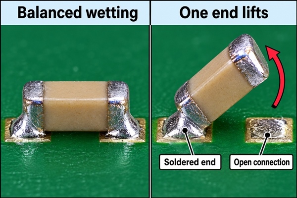
PCB tombstoning is a mounting defect in which a two-terminal chip stands on one end or tilts upward like a drawbridge. One termination remains attached while the other loses its intended connection. A fully vertical chip is easy to recognize, but a partially lifted component can also create an open circuit.
The terms Manhattan effect and drawbridge effect describe closely related appearances. A tombstone defect in SMT is not the same as a component that has merely shifted sideways. Inspect its orientation and both terminations before assigning the defect code. Electrical symptoms depend on the circuit: an open series resistor can interrupt a signal, while a disconnected bypass capacitor may leave the product functioning but with inadequate decoupling.
Why Does One End of a Component Lift During Reflow?
Molten solder wets the termination surfaces and applies forces to the chip. If one joint wets before the other, or the forces and their moment arms are unequal, a rotating moment can lift the opposite end. Uneven wetting explains the movement; the investigation must still establish what produced it.
Different solder quantities, pad geometries, termination conditions and heating histories can all contribute. A component photograph shows the final position, not the order in which its joints melted. A recurring lifted end beside a copper plane is a reason to investigate thermal imbalance, not proof that the plane alone caused the failure.
Which Components Are Most Susceptible to Tombstoning?
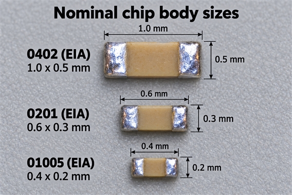
Small chip resistors and ceramic capacitors are common examples because their low mass offers little resistance to a wetting-force imbalance. 0201 tombstoning and 0402 tombstoning require particular attention to printing consistency and placement overlap. These package names must include their sizing convention: an imperial 0402 is not the same size as a metric 0402.
| Imperial / EIA designation | Metric designation | Nominal body length × width | Assembly consideration |
|---|---|---|---|
| 0402 | 1005 | 1.0 × 0.5 mm | Check both termination overlaps and copper connections. |
| 0201 | 0603 | 0.6 × 0.3 mm | Small absolute print or placement differences become significant. |
| 01005 | 0402 | 0.4 × 0.2 mm | Confirm package-specific printing, placement and inspection capability. |
These are nominal body dimensions, not land-pattern dimensions or acceptance tolerances. Use the exact component drawing for height, termination length and recommended footprint. A tombstoned resistor and a capacitor of the same nominal package need not behave identically; termination construction and solderability also matter. Other two-terminal devices can lift as well, so the diagnosis should follow the actual package rather than assume that all affected parts are capacitors.
How Do PCB Pads and Copper Connections Affect Tombstoning?
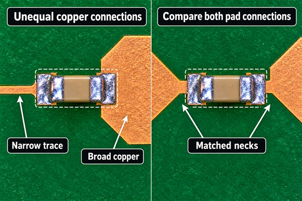
Start with the component manufacturer’s recommended land pattern. Compare pad length, width, spacing and exposed solderable area at the two ends. Oversized or asymmetric pads can change the solder shape and force acting on the terminations. Reducing pad size indiscriminately can trade a tombstone problem for insufficient attachment.
Next compare the copper connected to each pad. One pad tied directly to a broad plane and another connected by a narrow trace may have different thermal responses. Internal copper, nearby vias and the surrounding component population also belong in that comparison. On our FR4 PCBs, this means checking the relevant copper layers, not just matching the two rectangles visible on the top layer.
Matched connections or thermal reliefs may reduce the difference, but they must still satisfy current capacity, grounding and signal requirements. Unfilled vias close to a solderable pad can also disturb the available solder volume. Review the pad, mask opening and via treatment together instead of changing one feature without checking its effect on the others.
Can Uneven Solder Paste Cause Tombstoning?
Yes. Different paste deposits can leave one termination sitting higher or contacting less paste before reflow. After melting, the unequal solder volumes can also change the joint forces. Examine solder paste volume, height and deposit position as a pair rather than reviewing only the board-wide average.
Aperture blockage, stencil registration, underside contamination and inconsistent release can produce local differences. A nominally symmetric stencil does not guarantee symmetric printed deposits. Our SMT stencil service supports the aperture design needed for the component and board; the printed result still needs verification on the actual assembly.
Reducing excess paste at the outer ends of a chip can be a useful trial when solder volume is the identified contributor. Do not apply a universal aperture reduction to every package. Check the resulting fillets, attachment and printing repeatability, and ensure that a reduction does not introduce opens or poor wetting elsewhere.
How Can Placement Errors Create a Tombstone Defect?
Offset or skew can give the two terminations unequal overlap with their paste deposits. A placement-height error can leave one end without proper contact even when the camera image appears centered. Check the package definition, nozzle condition, pickup, local board support and placement settings for the affected reference designators.
Do not depend on solder self-alignment to correct a chip placed beyond its process tolerance. Equally, increasing placement force without checking the component limits can damage a ceramic body or squeeze paste out of position. Retain the pre-reflow image when possible: it helps separate a chip that was already misplaced from one that rotated during melting.
How Should You Adjust the Reflow Profile to Reduce Tombstoning?
Measure the assembly before changing the oven recipe. The oven-zone setpoints are not the temperature history at the two joints. Compare the affected area with a stable area and assess whether the joints approach melting at different times. On very small chips, sensor size and attachment can perturb the measurement, so profiling needs a suitable instrumented board and a consistent method.
An appropriate preheat or soak can reduce temperature differences, but extending it indefinitely can consume flux activity or exceed a material’s recommended exposure. Keep the profile inside both the selected solder paste window and component limits. A hotter peak cannot repair an unsuitable footprint or unequal paste deposits.
Atmosphere and alloy changes also require a controlled trial. Nitrogen can accelerate wetting, which may aggravate an existing imbalance; it is not automatically a tombstoning cure. Conversely, switching to air may affect other joints on the board. Compare the complete assembly result rather than optimizing only the lifted component.
Which Parameters Should You Record When Investigating Tombstoning?
Record measurements at the affected component, paired with a known-good position or build. The following parameters separate dimensional, printing, placement and thermal contributors. Numerical acceptance limits must come from the selected component, paste and qualified assembly process, not from a generic tombstoning checklist.
| Parameter | Unit or calculation | What to record | How to use it |
|---|---|---|---|
| Body and termination dimensions | mm | Part number, package convention, body length/width and termination dimensions | Confirm the correct land pattern and placement definition. |
| Pad and mask geometry | mm; mm² | Length, width, gap and exposed area at both ends | Separate drawing symmetry from the actual exposed pads. |
| Stencil aperture and thickness | mm or µm | Aperture dimensions, shape, foil thickness and revision | Check nominal deposit design and local release behavior. |
| Printed paste volume | mm³ | V1 and V2 from the paired pads | Compare individual deposits, not only a board average. |
| Relative volume difference | 100 × |V1 − V2| / [(V1 + V2) / 2] | Percentage plus the original volumes | Compare trials consistently; this formula is not a pass/fail standard. |
| Paste height and position | µm; X/Y offset in mm | Both deposits and their position relative to pads | Identify unequal seating or print registration. |
| Placement | X/Y in mm; rotation in degrees | Actual offset, skew and approved Z-height/force settings | Check termination overlap before reflow. |
| Temperature history | °C and seconds | Measurement locations, preheat, peak and time above the alloy’s liquidus | Compare the actual profile with material limits. |
| Heating rate | °C/s | Temperature interval and measurement method | Identify rapid changes without confusing zone settings with board temperature. |
| Defect frequency | Defective components / inspected opportunities | Reference designator, panel position, lot and trial size | Check whether the corrective action improved repeatability. |
For example, illustrative paste volumes of 0.008 and 0.010 mm³ give a relative difference of 22.2% using the formula above. That calculation quantifies the mismatch; it does not establish that 22.2% is an acceptable or unacceptable production limit. Retain the measurement system settings and the absolute volumes when comparing results.
How Do You Find the Root Cause of Repeated Tombstoning?
Start with the distribution of defects. Repetition at one reference designator suggests a different investigation from random defects across many identical chips. A problem confined to one panel edge may involve support, printing or heating conditions. A change coinciding with a new reel, paste lot or stencil revision gives another testable lead.
- Preserve the evidence. Record the lifted end, board orientation, reference designator and lot before rework.
- Check the pre-reflow condition. Compare paired SPI measurements and placement images.
- Compare the design. Inspect pad geometry, copper connections, vias and the component drawing.
- Check material and thermal history. Review paste handling, termination condition and the measured profile.
- Change one identified factor in a controlled trial. Record the other settings, sample size and defect count.
- Verify the full board. Confirm that fewer tombstones did not introduce bridging, insufficient solder or other defects.
AOI can flag component position and visible joint abnormalities, while microscope review helps confirm the physical condition. Electrical testing establishes the resulting circuit behavior but does not identify whether printing, placement or heating caused it. Use the records together; neither a single AOI image nor a passing functional test closes the root-cause investigation.
Tombstoning vs Solder Bridging and Cold Joints: What Is the Difference?
| Condition | Physical distinction | Likely electrical concern | Inspection focus |
|---|---|---|---|
| Tombstoning | One end of the chip lifts from its intended pad | Open connection or loss of that component’s function | Orientation and attachment at both terminations |
| Solder bridging | Solder connects conductors that should be separate | Unwanted short circuit | Clearance and continuity between adjacent nets |
| Poorly formed or cold joint | A joint has not formed properly; the component need not be upright | Open, high resistance or unstable connection | Wetting, joint integrity and process history, not gloss alone |
| Billboarding | A chip rolls onto its narrow side | Depends on termination contact and assembly requirements | Body orientation and the specified mounting condition |
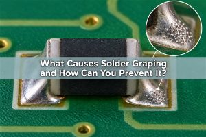
| Solder graping | Fine solder particles remain uncoalesced around a deposit | Joint-quality concern distinct from chip rotation | Particle coalescence and the surrounding joint |
A solder bridge in PCB assembly is therefore not another name for a tombstone. Several defects can coexist on the same board, but each needs its own evidence. A dull lead-free joint alone does not prove cold soldering, and an upright component alone does not prove that the reflow peak was too low.
How Do You Repair a Tombstoned Component?
Use an approved rework method compatible with the component and PCB. First isolate the board from power, follow ESD controls and inspect the chip, pads and nearby parts. A cracked body, damaged termination or lifted land needs disposition rather than simply pushing the component flat.
For a reusable component, the rework process must release it without mechanical force against solid solder, restore a suitable solder amount, and position both ends correctly. Replacement is appropriate when component integrity is uncertain or the assembly requirements demand it. Heating tools, preheat and exposure limits depend on the actual package and board.
After rework, inspect both joints and check the relevant electrical function. Record the repaired location and any required cleaning or retest. A successful individual repair does not demonstrate that the production cause has been removed; the next build still needs the corrective-action trial.
How Can Our PCB Assembly Process Help Control Tombstoning?
Our PCB assembly services include DFA review, stencil fabrication, solder paste printing, 3D SPI, placement, reflow, AOI and functional testing. We support SMD packages down to 01005, with the actual assembly requirements reviewed against the component, footprint and inspection needs.
For a tombstoning investigation, these stages provide different evidence: SPI checks the printed deposit, placement review checks the chip before melting, and post-reflow inspection checks the completed attachment. Our equipment includes a SINIC-TEK S8080 3D SPI system and SINIC-TEK A510DL 3D AOI system. The equipment does not replace a project-specific process window or the agreed acceptance requirements.
Send us the PCB files, BOM with exact manufacturer part numbers, placement data and assembly drawing. For an existing defect, include clear photographs, affected reference designators, failure counts and available printing or profile records. We can then discuss the board and assembly requirements for your build. Contact sales@bestpcbs.com for PCB fabrication and assembly support.
For a tombstoning PCB problem on your build, include the affected component locations and inspection records with your assembly inquiry.
Tombstoning PCB FAQs
Can a board with a tombstoned capacitor still power on?
Yes. A disconnected decoupling capacitor may not stop startup, even though the circuit has lost part of its intended filtering. Power-on alone is not an acceptance test for the assembly.
Does lead-free solder always cause more tombstoning?
No. The actual alloy’s melting behavior, paste formulation and the joint-to-joint imbalance matter. Do not treat all lead-free alloys as one process or assume that changing alloy fixes a footprint problem.
Should every tombstone be blamed on the assembly operator?
No. Design geometry, component condition, printed paste, placement and thermal history can contribute. Preserve the evidence and identify the process contribution before assigning corrective action.