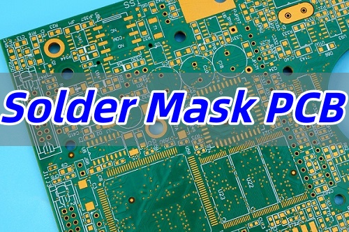
Why PCB is green? Most printed circuit boards are green because green solder mask became the most practical, stable, and production-friendly option for PCB manufacturing. The color itself does not make the circuit work better. The real value comes from the solder mask layer: it protects copper traces, reduces solder bridging, improves visual inspection, supports automated optical inspection, and keeps board production consistent.
For many OEM buyers, engineers, and hardware teams, green remains the default PCB color because it is widely available, cost-effective, easy to inspect, and suitable for most electronic products. Other colors such as black, white, blue, red, yellow, and purple can also be used, but they should be selected for a clear design, branding, lighting, or assembly reason.
What Is a Green PCB?
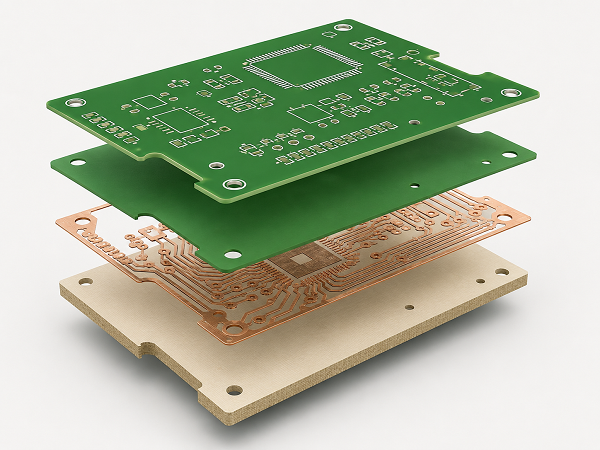
A green PCB is a printed circuit board covered with green solder mask. The base material under the surface may be FR4, aluminum substrate, copper substrate, ceramic substrate, polyimide, Rogers laminate, or another PCB material. The board looks green because the solder mask pigment is green, not because the copper, laminate, or circuit itself is green.
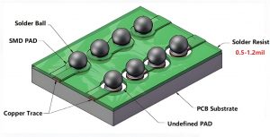
Solder mask is a thin protective coating applied over copper traces. It leaves pads, vias, test points, and soldering areas exposed according to the design files. This layer helps prevent oxidation, solder shorts, contamination, and handling damage.
In practical manufacturing, “green PCB” usually means:
| Item | Meaning |
|---|---|
| Green surface | Green solder mask |
| Conductive layer | Copper circuit traces |
| Base material | FR4, aluminum, ceramic, flex material, or others |
| White markings | Silkscreen for component labels and polarity marks |
| Exposed metal areas | Pads or holes with surface finish such as HASL, ENIG, OSP, immersion silver, or immersion tin |
A green PCB is not a special electrical category. It is simply the most common solder mask color used on printed circuit boards.
Why PCB Is Green?
PCB is green mainly because green solder mask offers a strong balance of manufacturing stability, visual contrast, inspection convenience, material availability, and cost control. Over time, PCB factories optimized their processes around green solder mask, and it became the standard option for mass production.
There are several practical reasons:
| Reason | Practical Meaning |
|---|---|
| Mature process | Green solder mask has been used for decades, so process control is stable. |
| Good contrast | Copper traces, pads, vias, and white silkscreen are easier to inspect. |
| Lower cost | Green solder mask is widely stocked and commonly processed. |
| Stable yield | Factories have mature exposure, development, curing, and inspection settings for green. |
| Easy repair and review | Defects such as scratches, bridges, exposed copper, and mask shift are easier to find. |
The short answer is simple: green is not mandatory, but it is efficient. For high-volume PCB production, small efficiency gains matter. A color that supports faster inspection, predictable production, and lower setup complexity naturally becomes the industry default.
Why Is Solder Mask Important in PCB Manufacturing?
Solder mask is one of the most important protective layers on a PCB. Without it, copper traces would be exposed to air, moisture, flux residue, handling contamination, and accidental solder contact. That would increase the risk of oxidation, corrosion, leakage, solder bridging, and short circuits.
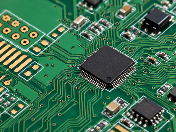
During PCB assembly, solder mask also helps control where solder flows. It creates a physical and visual boundary between solderable pads and non-solderable copper areas. This is especially important for fine-pitch ICs, BGA pads, QFN packages, dense SMT layouts, and high-reliability industrial boards.
A good solder mask should support:
| Function | Why It Matters |
|---|---|
| Electrical insulation | Helps prevent unintended contact between copper features |
| Copper protection | Reduces oxidation and environmental exposure |
| Solder control | Limits solder spread during assembly |
| Visual inspection | Helps operators identify defects more easily |
| AOI compatibility | Supports automated inspection contrast |
| Long-term reliability | Protects the board during service life |
In other words, PCB color is visual, but solder mask performance is functional. Buyers should care less about the color itself and more about solder mask adhesion, registration accuracy, curing quality, cleanliness, and compatibility with the final application.
How Does Green Solder Mask Work?
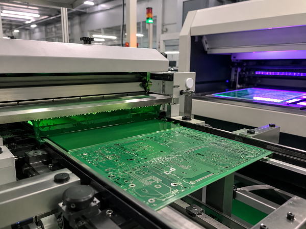
Green solder mask works by coating the PCB surface with a polymer material that covers selected copper areas while leaving soldering pads open. In standard PCB fabrication, liquid photoimageable solder mask is commonly used for rigid PCBs. The mask is applied, dried, exposed with UV light, developed, cured, and inspected.
A simplified process looks like this:
| Process Step | Purpose |
|---|---|
| Surface preparation | Cleans copper and improves mask adhesion |
| Solder mask coating | Applies mask over both sides of the PCB |
| Pre-bake | Removes solvent and stabilizes the coating |
| UV exposure | Defines areas to keep and areas to open |
| Development | Removes unexposed or unwanted mask areas |
| Final curing | Hardens the solder mask for durability |
| Inspection | Checks coverage, registration, bubbles, scratches, and exposed copper |
The green pigment helps the mask appear clearly under normal lighting and inspection systems. For many factories, green also performs well during exposure and development because the process window is familiar and stable.
This is why green is often preferred for production boards that need dependable output rather than special appearance.
What Materials Are Used in Green PCB Solder Mask?
Most modern green solder masks are made from photoimageable polymer systems. The exact formulation depends on the solder mask supplier, PCB application, curing process, and reliability requirement. For common rigid boards, liquid photoimageable solder mask is widely used because it supports fine features and efficient mass production.
Common solder mask material considerations include:
| Material Factor | Engineering Concern |
|---|---|
| Resin system | Adhesion, hardness, chemical resistance |
| Pigment | Color, light absorption, inspection contrast |
| Filler | Mechanical stability and coating behavior |
| Photoinitiator | UV exposure response |
| Solvent system | Coating and drying performance |
| Final cure property | Heat resistance, insulation, and durability |
For flexible PCBs, coverlay or flexible solder mask may be used depending on the bending requirement. For high-reliability applications, the solder mask should be selected according to the operating environment, soldering temperature, chemical exposure, voltage spacing, and applicable customer standards.
The color is only one part of the formulation. A poor-quality green solder mask can still fail. A high-quality blue, black, or white solder mask can also perform well if it is correctly specified and processed.
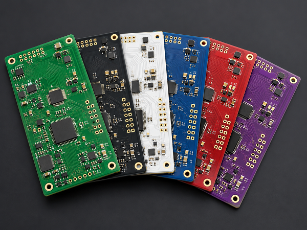
What Are the Main PCB Solder Mask Colors?
Green is the most common PCB solder mask color, but it is not the only choice. PCB manufacturers can produce boards in several colors, depending on material availability, process control, and project requirements.
| Solder Mask Color | Common Use | Practical Notes |
|---|---|---|
| Green | General electronics, industrial PCBs, prototypes, mass production | Best balance of cost, availability, and inspection |
| Black | Consumer electronics, display products, premium visual design | Attractive, but harder to inspect |
| White | LED lighting, backlight modules, reflective applications | Good light reflection, but stains and defects show easily |
| Blue | Development boards, communication products, industrial controls | Good visual identity and acceptable inspection contrast |
| Red | Demo boards, power boards, brand-specific products | Clear appearance, moderate inspection convenience |
| Yellow | Special identification or testing boards | Less common, may need longer lead time |
| Purple | Brand-specific or custom projects | Often selected for visual differentiation |
| Matte colors | Products needing low reflection | Useful in optical or appearance-sensitive products |
For most functional electronics, solder mask color has little direct effect on circuit performance. However, it can affect inspection speed, defect visibility, lead time, and production cost.
Green PCB vs Other PCB Colors: Which One Should You Choose?
Green is usually the safest choice when cost, lead time, inspection reliability, and production stability matter. Other colors can be useful, but they should be selected with a clear purpose.
| Color Option | Advantages | Possible Limits | Best Fit |
|---|---|---|---|
| Green | Low cost, easy inspection, stable process | Less unique appearance | Most PCB projects |
| Black | Premium look, hides surface details | Harder AOI and manual inspection | Consumer devices, visible boards |
| White | High reflectivity | Easier to stain, lower contrast for some markings | LED and lighting products |
| Blue | Good branding and readable silkscreen | May cost more than green | Industrial and development boards |
| Red | Strong visual identity | Less common than green | Power modules, demo boards |
| Matte black | Low reflection | More difficult defect review | Optical devices, camera-related products |
For engineering samples, green is often recommended unless the product needs a specific color for function or appearance. For bulk production, buyers should confirm whether the selected color affects MOQ, cost, solder mask brand, process lead time, and cosmetic acceptance criteria.
Does Green PCB Perform Better Electrically?
Green PCB does not automatically perform better electrically. Electrical performance is mainly determined by the laminate material, copper thickness, trace geometry, dielectric constant, surface finish, impedance control, via structure, cleanliness, and manufacturing quality.
The solder mask can influence certain details, especially in high-voltage, high-frequency, fine-pitch, and harsh-environment applications. However, the color itself is not the key factor. The mask’s insulation resistance, adhesion, thickness, curing quality, and cleanliness are more important than whether it is green, black, blue, or white.
| Performance Area | Main Factor |
|---|---|
| Impedance control | Stack-up, dielectric constant, trace width, spacing |
| Current carrying capacity | Copper thickness, trace width, thermal design |
| High voltage insulation | Clearance, creepage, solder mask quality |
| RF performance | Laminate type, copper roughness, layout, solder mask opening strategy |
| Thermal performance | Substrate material, copper area, via design, heat path |
Green is preferred because it is practical, not because it creates superior electrical performance. For standard FR4, aluminum PCB, rigid-flex PCB, and many multilayer boards, green simply provides a stable and economical surface solution.
What Manufacturing Defects Can Solder Mask Help Prevent?
Solder mask helps prevent several common PCB and PCBA defects. This is one reason it is critical in both bare board fabrication and assembly.
| Defect | How Solder Mask Helps |
|---|---|
| Solder bridging | Keeps solder from spreading between adjacent pads |
| Copper oxidation | Covers copper traces and reduces exposure |
| Short circuits | Adds insulation between conductive areas |
| Flux contamination risk | Helps protect non-solderable copper areas |
| Handling damage | Reduces direct contact with copper |
| Tin spreading | Controls solder wetting area |
| Assembly misjudgment | Improves visibility of pads, labels, and component positions |
For fine-pitch components, solder mask registration is especially important. If the mask opening is too large, solder may flow where it should not. If the opening is too small or shifted, pads may be partially covered, causing poor solderability, insufficient wetting, tombstoning, or open joints.
A reliable PCB factory checks solder mask alignment, thickness, curing, adhesion, and surface condition before shipment.
What Are Common Green PCB Failure Issues?
Green PCB failures are usually not caused by the green color. They are caused by solder mask material problems, process control issues, poor design clearance, contamination, or harsh operating conditions.
| Failure Issue | Possible Cause | Result |
|---|---|---|
| Solder mask peeling | Poor surface preparation or weak curing | Exposed copper, reliability risk |
| Mask blistering | Moisture, contamination, or baking issue | Surface bubbles after reflow |
| Exposed copper | Misregistration, scratches, insufficient coverage | Oxidation or short risk |
| Solder mask bridge missing | Poor design or process limitation | Solder bridging during assembly |
| Pad contamination | Mask residue on pads | Poor solder wetting |
| Cracking | Thermal stress or poor flexibility | Exposure and insulation risk |
| Color inconsistency | Batch variation or curing difference | Cosmetic rejection |
In production, engineers should not judge solder mask only by color uniformity. More important checks include adhesion, registration, cure level, insulation performance, cleanliness, and whether the mask meets the product’s use environment.
How Is Green PCB Tested and Inspected?
Green PCBs are inspected through both visual and electrical methods. For standard production, inspection normally includes solder mask appearance review, AOI, electrical testing, dimensional measurement, and final quality control.
| Inspection Item | What It Checks |
|---|---|
| Visual inspection | Scratches, bubbles, peeling, exposed copper, stains |
| AOI | Open circuits, shorts, line defects, registration issues |
| Electrical test | Net continuity and isolation |
| Solder mask adhesion test | Mask bonding to PCB surface |
| Solderability test | Pad wetting performance |
| Cross-section analysis | Layer structure, copper thickness, hole quality |
| Ionic contamination test | Cleanliness for reliability-sensitive boards |
| Thermal stress test | Resistance to soldering and heat cycles |
For higher-reliability projects, customers may specify IPC Class 2 or Class 3 workmanship requirements, IPC-SM-840 solder mask material qualification, IPC-A-600 bare board acceptance criteria, and application-specific test reports.
For automotive, medical, industrial control, aerospace support, and power electronics, solder mask inspection should be treated as part of reliability control, not only cosmetic review.
Where Are Green PCBs Used?
Green PCBs are used across nearly every electronics industry because the color is suitable for both prototypes and mass production. The applications are broad because green solder mask is not limited to one PCB type.
| Industry | Typical PCB Applications |
|---|---|
| Industrial control | PLC modules, power control boards, automation controllers |
| Automotive electronics | Lighting modules, sensor boards, control units, BMS boards |
| Medical electronics | Monitoring equipment, diagnostic devices, control modules |
| Consumer electronics | Home appliances, smart devices, audio products |
| Communication equipment | Routers, gateways, RF support boards, base station modules |
| LED lighting | Drivers, control boards, aluminum PCBs |
| Power electronics | Inverters, power supplies, charging systems |
| Aerospace and defense support | High-reliability control boards and interface boards |
In many of these products, customers choose green because it keeps engineering review simple and production risk lower. When the PCB is hidden inside an enclosure, green is often the most practical color.
Industrial Case: Why a Buyer Chose Green PCB for Mass Production
A European industrial equipment customer needed a 4-layer FR4 control PCB for a motor control cabinet. The first prototype used black solder mask because the customer wanted a more premium appearance. During assembly review, the factory found that black solder mask made fine scratches, residue, and certain solder mask registration issues harder to identify under normal inspection light.
For the next revision, the customer changed the solder mask to green. The electrical design did not change. However, inspection became faster, silkscreen readability improved, and defect review during trial production became more efficient. The customer kept green solder mask for bulk production because the PCB was installed inside the equipment and appearance was less important than stable manufacturing.
This case shows a common engineering point: if the board is not visible to the end user, green is often the better production choice. It reduces unnecessary process risk and keeps quality review straightforward.
Design Tips for Green PCB Solder Mask
Good solder mask quality starts from design. Even when using standard green solder mask, poor design rules can create assembly problems later.
Engineers should confirm these points before releasing Gerber files:
| Design Item | Recommendation |
|---|---|
| Solder mask expansion | Match the pad type, component pitch, and factory capability |
| Solder mask dam | Keep enough mask between fine-pitch pads where possible |
| Via tenting | Define whether vias are open, tented, plugged, or filled |
| BGA pads | Confirm SMD or NSMD pad strategy with the assembler |
| Silkscreen clearance | Avoid printing text on pads or exposed copper |
| High-voltage spacing | Do not rely only on solder mask for insulation safety |
| RF areas | Confirm whether solder mask should be removed over RF traces |
| LED boards | Check whether green or white mask better suits optical needs |
For dense SMT boards, the solder mask dam between pads can become very narrow. If the dam is below the factory’s stable capability, it may break during processing. This can increase solder bridge risk during assembly.
The best approach is to confirm solder mask rules with the PCB manufacturer before layout finalization.
Manufacturing Notes for Green PCB Production
From a factory perspective, green solder mask is easier to standardize because materials, exposure settings, inspection criteria, and operator experience are mature. Still, stable results depend on controlled manufacturing.
A reliable green PCB production process should control:
| Manufacturing Factor | Why It Matters |
|---|---|
| Copper surface treatment before coating | Improves solder mask adhesion |
| Coating thickness | Affects insulation, appearance, and registration |
| Exposure energy | Controls pattern definition |
| Development time | Prevents residue or over-development |
| Final curing | Ensures hardness, chemical resistance, and adhesion |
| Cleanroom control | Reduces dust, particles, and contamination |
| Color batch control | Improves cosmetic consistency |
| Final inspection | Prevents defective boards from reaching assembly |
For high-volume orders, customers should confirm whether the supplier keeps stable solder mask brands and documented process windows. Changing solder mask materials during production can create differences in gloss, color, adhesion, and curing behavior.
What Affects Green PCB Cost?
Green PCB is usually the most economical solder mask option because it is the standard color in many factories. However, the total PCB cost is not determined by color alone.
Major cost factors include:
| Cost Factor | Impact on Price |
|---|---|
| Layer count | More layers increase lamination and drilling cost |
| Board size | Larger panels consume more material |
| Copper thickness | Heavy copper requires more processing control |
| Surface finish | ENIG, ENEPIG, immersion silver, OSP, or HASL affect cost |
| Minimum trace/space | Fine lines require tighter process control |
| Hole size and via type | Blind vias, buried vias, filled vias, and microvias increase cost |
| Solder mask color | Non-standard colors may add cost or lead time |
| Testing requirement | Extra reliability tests increase production cost |
| Quantity | Higher volume improves panel utilization and unit cost |
| Lead time | Urgent production may require expedited processing |
If cost control is important, choosing standard green solder mask is often a smart decision. Buyers can reserve budget for more important performance factors such as laminate grade, copper thickness, impedance control, surface finish, testing, and assembly quality.
How Should OEM Buyers Choose PCB Color?
OEM buyers should choose PCB color based on project function, inspection needs, production volume, and product appearance. Green is suitable for most projects, but it is not always the only correct answer.
A simple selection guide:
| Project Requirement | Recommended Choice |
|---|---|
| Lowest cost and fastest delivery | Green |
| Internal control board | Green |
| High-volume industrial PCB | Green |
| Visible consumer electronics board | Black, blue, red, or custom color |
| LED reflection requirement | White |
| Optical low-reflection product | Matte black |
| Prototype review and debugging | Green or blue |
| Brand-specific visual identity | Custom color |
| Harsh-environment electronics | Select by solder mask performance, not only color |
Buyers should also ask whether the chosen color affects sample lead time, bulk price, MOQ, cosmetic standard, silkscreen readability, AOI reliability, and long-term supply stability.
For most B2B projects, color should support production quality first and appearance second.
How to Choose a Reliable Green PCB Manufacturer
A reliable PCB manufacturer should not only offer green solder mask. It should also understand solder mask design, process capability, testing standards, and application requirements.
Before placing an order, buyers should check:
| Supplier Checkpoint | What to Confirm |
|---|---|
| Factory capability | Layer count, copper thickness, minimum line width, solder mask dam |
| Material control | Laminate brand, solder mask brand, surface finish options |
| Quality system | ISO, IATF, medical, aerospace, or project-specific requirements |
| Inspection process | AOI, electrical test, visual inspection, microsection when needed |
| Engineering support | DFM review, stack-up review, solder mask opening review |
| Documentation | CoC, test report, material report, RoHS/REACH report |
| Batch consistency | Stable color, gloss, curing, and solderability |
| Global delivery | Packaging, logistics, export documentation, shipment tracking |
For international buyers sourcing from China, the key is not to find the cheapest quote. The better approach is to choose a source factory that can review design risks, support prototypes, stabilize bulk production, and provide clear communication before problems reach assembly.
What Should You Check Before Ordering Green PCB?
Before ordering green PCB prototypes or batch production, prepare complete manufacturing data and confirm key requirements with the supplier.
Recommended order checklist:
| Item | What to Provide or Confirm |
|---|---|
| Gerber files | Include copper, solder mask, silkscreen, drill, outline files |
| PCB stack-up | Layer count, thickness, material, copper weight |
| Solder mask color | Green gloss, green matte, or other color |
| Surface finish | HASL, lead-free HASL, ENIG, OSP, immersion silver, ENEPIG |
| Quantity | Prototype, pilot run, or mass production volume |
| IPC class | Class 2, Class 3, or customer-specific acceptance |
| Special requirements | Impedance, high voltage, RF, heat dissipation, bending, coating |
| Testing | E-test, AOI, FAI, microsection, thermal test, ionic contamination |
| Assembly plan | SMT, DIP, conformal coating, box build, functional test |
| Packaging | Vacuum packing, humidity card, desiccant, ESD protection |
Clear files and specifications reduce engineering questions, shorten quotation time, and prevent avoidable production delays.
Frequently Asked Questions About Why PCB Is Green
Why are most PCBs green?
Most PCBs are green because green solder mask is practical for manufacturing. It provides good contrast for inspection, works well with white silkscreen, supports mature production processes, and is widely available in PCB factories. The color itself does not improve circuit function, but it helps production teams inspect and control quality more efficiently.
Is a green PCB better than a black PCB?
A green PCB is usually easier to inspect than a black PCB. Black solder mask can look premium, but it may hide scratches, residue, exposed copper, and registration issues under normal lighting. If the board is inside a product, green is usually more practical. If the board is visible to users, black may be selected for appearance.
Does PCB color affect performance?
PCB color usually does not affect electrical performance directly. Performance depends more on laminate material, copper thickness, trace geometry, impedance control, surface finish, via design, and manufacturing quality. However, color can affect inspection, defect visibility, cost, lead time, and silkscreen readability. For critical boards, solder mask quality matters more than color.
Why is green solder mask cheaper?
Green solder mask is often cheaper because it is the default color in many PCB factories. Materials are commonly stocked, process settings are mature, and production teams are familiar with inspection standards. Non-standard colors may require extra setup, longer preparation, lower panel efficiency, or additional cosmetic review, especially for small and medium orders.
Can I choose another PCB color?
Yes. PCB solder mask can be black, white, blue, red, yellow, purple, or matte colors, depending on the manufacturer’s capability. You should choose another color only when it supports appearance, branding, LED reflection, optical performance, or product differentiation. For normal industrial and internal electronics, green remains the safest and most efficient option.
Why do LED PCBs often use white solder mask?
LED PCBs often use white solder mask because white reflects light better than green or black. This can improve optical efficiency in lighting products, backlight modules, and LED panels. However, white solder mask may show stains, scratches, and flux residue more easily. Buyers should balance reflectivity, cleanliness control, and cosmetic acceptance standards.
Is solder mask the same as PCB coating?
Solder mask is a permanent protective layer applied during PCB fabrication. It is different from conformal coating, which is usually applied after PCB assembly to protect components and solder joints from moisture, dust, chemicals, and harsh environments. A board can have both solder mask and conformal coating when the application requires extra protection.
What happens if a PCB has no solder mask?
A PCB without solder mask has exposed copper traces, which can oxidize, contaminate, or short more easily. During soldering, solder may spread beyond the intended pads and create bridges. Some simple prototypes or special boards may use no solder mask, but most production PCBs need solder mask for reliability, assembly control, and protection.
Does green PCB mean the board is environmentally friendly?
No. Green PCB usually refers to the color of the solder mask, not environmental performance. Environmental compliance depends on material selection, lead-free process, RoHS compliance, REACH compliance, waste control, and supplier management. A green-colored PCB is not automatically more sustainable than a blue, black, or white PCB.
What is the best solder mask color for prototypes?
Green is often the best solder mask color for prototypes because it is affordable, fast, and easy to inspect. Engineers can clearly see pads, traces, silkscreen, and possible defects. Blue is also a good option for development boards. Black or white may look better, but they can make inspection and rework less convenient.
Can solder mask color affect AOI inspection?
Yes. Solder mask color can affect AOI because different colors create different contrast under inspection lighting. Green usually provides stable contrast for copper features, pads, and white silkscreen. Black and white boards may require more careful inspection settings. For fine-pitch or high-volume boards, confirm AOI compatibility before choosing a non-standard color.
Why do some premium electronics use black PCBs?
Some premium electronics use black PCBs because black gives a clean, high-end appearance, especially when the board is visible through a case or used in consumer devices. The choice is usually aesthetic or brand-related. From a production viewpoint, black can be harder to inspect, so it should be selected with proper quality control.
What solder mask color should I choose for industrial control PCBs?
For industrial control PCBs, green is usually the best choice unless there is a specific appearance, optical, or customer requirement. It supports stable manufacturing, clear inspection, readable silkscreen, and cost control. Industrial boards often focus on long-term reliability, traceability, and assembly quality, so practical production advantages matter more than visual uniqueness.
How do I specify green solder mask in PCB files?
In most cases, Gerber files define solder mask openings, while the color is specified in the order notes or fabrication drawing. You can write “green solder mask, white silkscreen” and add gloss or matte if needed. For high-reliability projects, also specify IPC class, solder mask type, surface finish, testing requirements, and cosmetic acceptance criteria.
What should buyers ask a PCB supplier about solder mask?
Buyers should ask about solder mask color options, solder mask brand, minimum solder mask dam, registration capability, via tenting options, IPC compliance, surface finish compatibility, and inspection standards. For bulk production, also confirm whether the supplier will keep the same solder mask material and process settings to maintain consistent appearance and quality.
Conclusion
PCB is green because green solder mask gives manufacturers, engineers, and buyers the best practical balance of cost, inspection clarity, process stability, and production availability. The color does not make the circuit electrically stronger, but it helps factories control quality more efficiently and helps engineers review boards more easily.
For most OEM projects, green solder mask is the recommended default. Choose another color only when it serves a clear purpose, such as LED reflection, consumer product appearance, optical requirements, or brand identity. When reliability matters, focus on solder mask quality, registration, adhesion, curing, cleanliness, IPC acceptance criteria, and supplier process control.
For procurement teams, the best decision is to work with a PCB source factory that can support DFM review, prototype development, stable batch production, documented quality control, and global delivery without unnecessary middleman layers.