If S11 changes every time you reconnect an SMA edge launch, start with the cable, mating interface and calibration before changing the PCB. If the same mismatch survives repeat mating and follows one launch or board revision, check seating, ground contact and the transition geometry.
Consider a hypothetical 50 Ω RF coupon with two end launches and a line between them. One unit shows a notch in input return loss and another behaves differently. The goal is to isolate a repeatable board effect from a measurement or assembly effect—not to qualify a connector from its catalog frequency alone.
sma edge launch connector
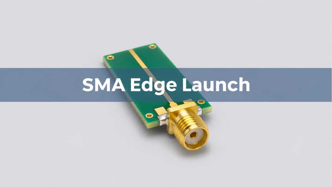
An SMA edge launch joins a coaxial line to a transmission line at the PCB edge. The center contact feeds the signal trace and the outer body connects to the board reference through its ground contacts. A 50 Ω cable and a 50 Ω trace do not guarantee that the transition between them is 50 Ω.
Before testing the coupon, identify the connector part, whether it is soldered or mechanically clamped, the cable mating plane and the intended reference plane. See the SMA terminal PCB guide for general mounting options; the procedure here is specifically for diagnosing the edge transition.
sma edge mount connector dimensions
Use the exact connector drawing and PCB layout, not just the SMA interface specification. The Samtec SMA series catalog is one example of a named 50 Ω connector to review with its own drawings. Do not substitute dimensions from that part for a similar-looking clamp-on assembly.
| Parameter | What to record | Why it matters |
| Impedance | 50 Ω nominal in this example | Does not specify launch behavior |
| Thickness | Finished local range in mm | Determines seating and contact |
| Edge position | Pad setback and profile tolerance in mm | Controls pin overlap |
| RF band | Defined sweep limits in GHz | Sets comparison range |
| Return loss | Project mask in dB at a stated plane | Defines pass or fail |
edge launch sma connector for 0.8 mm
A connector listing for a 0.8 mm board is a starting point, not a fit tolerance. Check the manufacturer’s permitted finished board thickness and whether any surface relief or mask restriction applies. A board sold as 0.8 mm can still have a stated tolerance that exceeds the connector’s permitted range.
For example only, if the released stackup is 0.80 ± 0.08 mm and a hypothetical connector allows 0.75–0.85 mm, the PCB window is 0.72–0.88 mm. These ranges do not nest. Tighten the agreed local thickness, choose a compatible connector, or qualify a controlled combination; do not approve the nominal match alone.
sma edge mount footprint
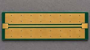
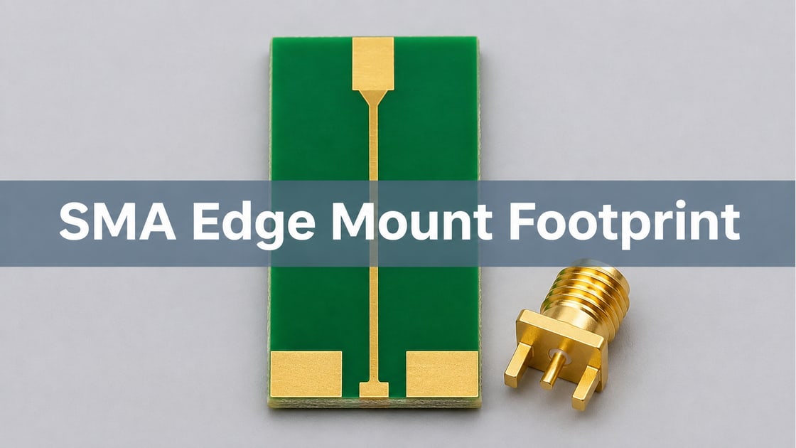
Review the center contact, adjacent ground, first section of line and nearby reference vias as one transition. Compare the final profile and copper artwork against the connector footprint on the same coordinate system. A correctly sized trace can still enter the pin through a long pad, a cutout or a poor ground connection that changes the local impedance.
Save a side view of connector seating and check the ground contacts against the installation drawing. If one edge is offset, compare the bad coupon with a known-good unit before changing trace width. This separates a fabrication or assembly deviation from the geometry common to every board.
solderless sma connector
Use a removable clamp-on launch when the fixture calls for controlled swapping or rework and the board matches the connector’s contact geometry. Use a soldered launch when the selected connector and product require permanent attachment. Compare the implementations on matched coupon designs where possible; a change in footprint can otherwise be mistaken for a change in attachment method.
| Option | Primary reason to use it | Failure to check |
| Clamp-on launch | Removable fixture connector | Seat and clamp repeatability |
| Soldered launch | Permanent assembly | Contact wetting and consistent pin position |
| Keep launch and fix setup | Result changes with the test setup | Repeatable mating and calibration verification |
how to solder sma connector to pcb
For a soldered part, follow the installation procedure for that exact component. Fixture it against the specified board edge, confirm center-pin alignment and inspect all required ground connections. Keep solder volume consistent with the approved procedure. Extra solder is not a reliable RF correction and can change transition geometry.
Capture the first article from the side and top. Record the connector revision, fixture and assembly conditions before comparing units. If a suspicious connection is reworked, remeasure before and after under the same cable and calibration so that any improvement can be attributed to the change.
rf connector torque specifications
Use the connector and cable maker’s instructions for the specific hardware. Coupling torque at a coax interface is not the same setting as clamp screw torque on a removable launch. Hold the connector body as specified so cable rotation does not twist the board. Southwest Microwave’s installation guidance illustrates why the assembly procedure is part-specific.
Start with a calibrated verification device or known-good reference. Keep cable routing fixed. Capture, disconnect and reconnect using the approved procedure, and save repeat sweeps. If the variation follows one cable or adapter, replace or repair that setup component before comparing board revisions.
pcb edge launch connector
Set the VNA reference plane and sweep limits before comparing boards. If calibration stops at the coax mating plane, the launch remains part of the result. Port extension can move an electrical reference under its model assumptions; it does not automatically remove a mismatched launch. Use a validated fixture-removal method only if you need to separate launch and line.
As a teaching example, a 15 dB return-loss requirement corresponds to a reflection magnitude of 10−15/20 ≈ 0.178. If the same coupon measures 17 dB after one mate and 11 dB after another at the critical frequency, it is not a repeatable pass. Fix the measurement or mounting inconsistency, then require the agreed S11 mask across the full band and repeated assemblies. Also check S21 if the insertion-loss budget matters.
FAQ
Is an SMA connector marked 50 Ω enough for a matched launch?
No. Its nominal interface impedance does not guarantee the PCB transition. The center pad, line geometry, return contacts and local board thickness affect the launch. Use the footprint for the exact part and verify the assembled transition across the frequency band that matters to the product.
Is edge launch the same as edge mount?
The terms often overlap, but the part drawing determines what the connector actually needs. Some parts use soldered ground contacts and others clamp around a board edge. Match the part number, orientation, pad layout and finished thickness rather than relying on a catalog description or a similar photograph.
Can I use the same footprint for 0.8 mm and 1.6 mm boards?
Do not assume so. A change in thickness can affect pin seating, local impedance and the ground-contact geometry. Confirm both the connector’s allowed finished thickness and the transmission-line stackup. Even when a connector family offers both sizes, the exact part and footprint may differ.
Should I judge the launch from a continuity test?
Continuity can catch an open or short, but it cannot show how an assembled transition reflects energy at RF. Use an agreed VNA measurement in addition to the mechanical and electrical inspection. Record the calibration plane and compare the result across the operating band, not just at one frequency.
Why does S11 change when I reconnect the cable?
Mating condition, connector cleanliness, coupling torque, cable motion and adapters can all affect repeatability. First verify the setup with a known reference, then repeat with the cable held in the same position. If the effect follows a particular coupon after that check, inspect its launch and mounting.
Is negative S11 the same as positive return loss?
When both are in decibels, return loss is commonly the negative of S11 magnitude in dB. Thus S11 of −15 dB corresponds to 15 dB return loss. Write which convention is in the release limit and confirm that all compared sweeps use the same reference plane.
Does port extension remove connector mismatch?
Not by itself. Port extension compensates electrical length and may include a loss model, but a physical impedance discontinuity can remain. If you need to report only the line, use a validated fixture removal procedure. Keep the as-assembled result when connector performance is part of the product requirement.
Can the two launches be separated from one through measurement?
Not uniquely from a single ordinary through sweep without additional assumptions or standards. The line and both transitions contribute. To localize a problem, compare end-swapped or matched coupons and use appropriate calibration or fixture characterization. Report what was measured directly and what was estimated from the method.
Technical References
- Samtec: SMA-J-P-H-ST-EM1
- Southwest Microwave: End Launch Connector Installation
- Keysight: Port Extensions
Request a Fabrication Review
For a Best Technology RF PCB review, send the stackup, connector part and drawing, edge footprint, and the intended test band and reference plane. sales@bestpcbs.com