





A PCB directional coupler samples RF traveling in one direction while rejecting signals traveling in the other. For forward power monitoring, choose a coupling factor that puts samples inside the detector’s usable range. For reflected power or VSWR, check directivity as well: a coupler can have exactly the intended coupling and still show a false reflection because forward energy leaks into the reverse channel.
Consider a four-port, 50 Ω monitoring board for a transmitter output. The goal is to measure a 25 dB load return loss across the operating band. Start with the reverse channel’s leakage budget, then choose a layout and a measurement setup that can actually show whether the board meets it.
What Is a Directional Coupler?
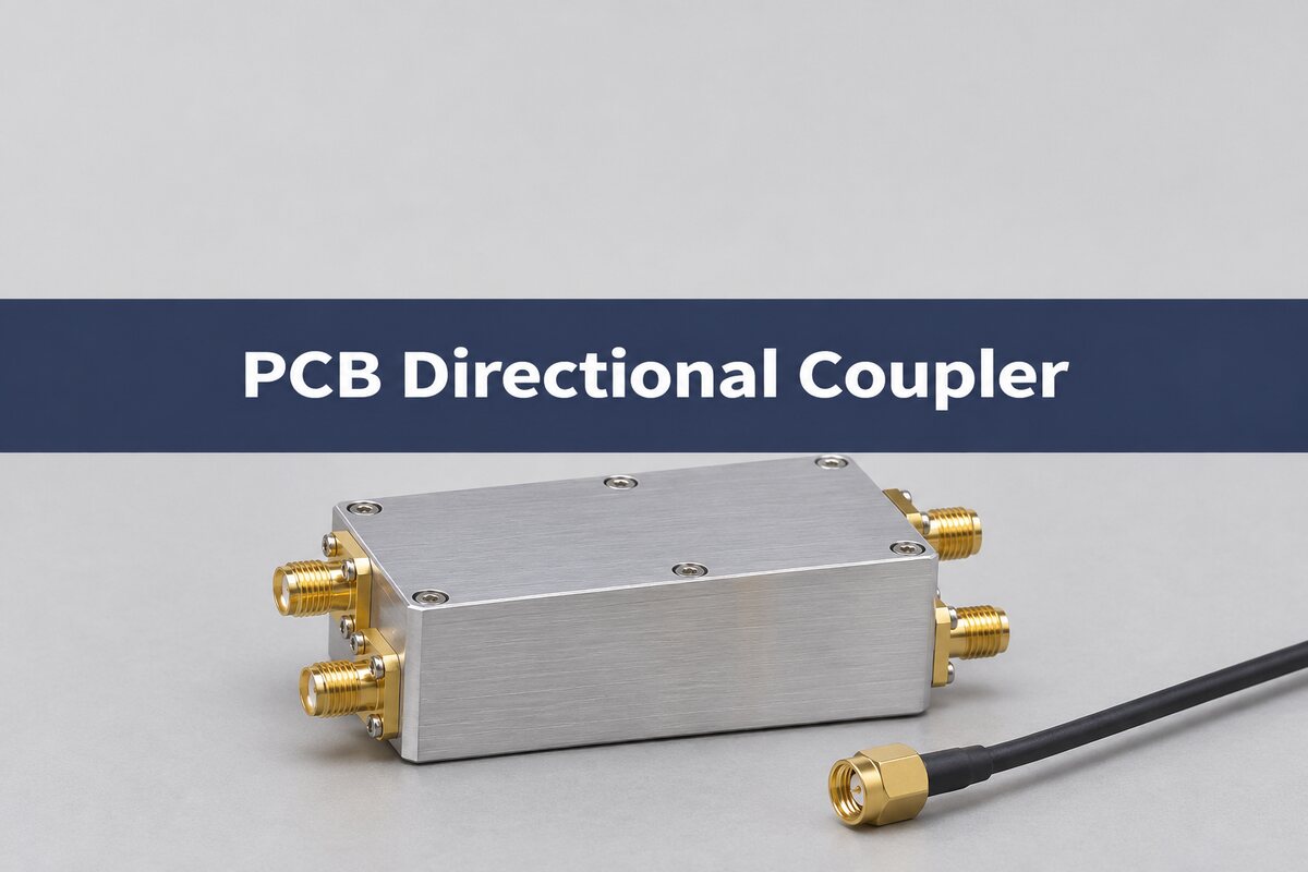
A directional coupler is a passive network with a through path and a sampling path. In a coupled-line version, fields from a driven trace induce signals on a nearby line without a direct copper connection. Waves on the sampling line combine differently at its two ends. One end receives the desired sample; the other ideally receives none for that direction.
For this article, P1 and P2 are the main-line ports. With power driven into P1, P3 is the forward sample and P4 is nominally isolated. Drive from P2 and the sample roles reverse. This numbering is a convention for the example; commercial drawings can number their ports differently. Match the drawing and the VNA port labels before interpreting a plot. See Mini-Circuits’ directional coupler application note for the underlying port relationships.
Directional Coupler vs Power Splitter: Which Does the Job?
Use the coupler when you need a small, direction-selective sample while the main RF path continues. Use a splitter when the task is to distribute an input among outputs; a splitter’s output-port isolation does not make it a directional reflection sampler. A packaged coupler is also a realistic alternative to etching coupled lines if board dimensions or validation effort make a custom geometry unattractive.
| Option | Choose it for | What to verify |
| Printed coupled lines | An integrated, reproducible RF sampling section on your stackup. | Finished gap, coupling across band, directivity and fixture repeatability. |
| Packaged directional coupler | A specified component when tight PCB coupling geometry is impractical. | Vendor test conditions, land pattern, port loading and board launch. |
| Power splitter | Distribution to two paths; an equal two-way split gives about 3 dB per output before excess loss. | Balance, loss and isolation; do not use it to infer direction. |
The practical choice for the transmitter is between the first two. Compare their demonstrated rejection of the forward signal across the intended band, not just nominal coupling at the center frequency. The Marki Microwave primer explains why sampled power and power division are different functions.
Directional Coupler Coupling Factor and Isolation
Coupling sets the desired sample level; isolation describes unwanted feedthrough. Express both as positive attenuation values in dB for the following example. A VNA normally plots the corresponding transmission terms as negative dB. Confusing one convention for the other can make a good isolation value appear worse during review.
| Parameter | Illustrative target | Why it matters |
| Reference impedance | 50 Ω at all four ports | Mismatch can change both the desired sample and leakage. |
| Coupling | 20 dB at a point in the band | About 1% of incident power reaches the desired sampling port. |
| Forward leakage into P4 | 50 dB attenuation | With 20 dB reverse coupling this gives 30 dB input-referenced rejection at P4. |
| Through loss and flatness | Specify separately over the operating band | One center-frequency result cannot verify band edges or detector headroom. |
With +10 dBm at P1 and 20 dB forward coupling, the idealized sample at P3 is −10 dBm. Use the expected power extremes and variation across the band to size the detector input. Do not add attenuation or increase coupling just to fix a poor reverse reading until you know whether the problem is detector range or directional leakage.
Microstrip Directional Coupler Design: Match the Stackup
Design the coupled section using the actual dielectric height, material properties, finished copper width, spacing and thickness. The gap changes how strongly the two lines interact; their length and dielectric environment determine the useful band. Equal and opposite excitation and equal in-phase excitation are the two basic modes of the coupled pair. In microstrip their phase velocities can differ, weakening cancellation at the isolated end even when the coupling looks good.
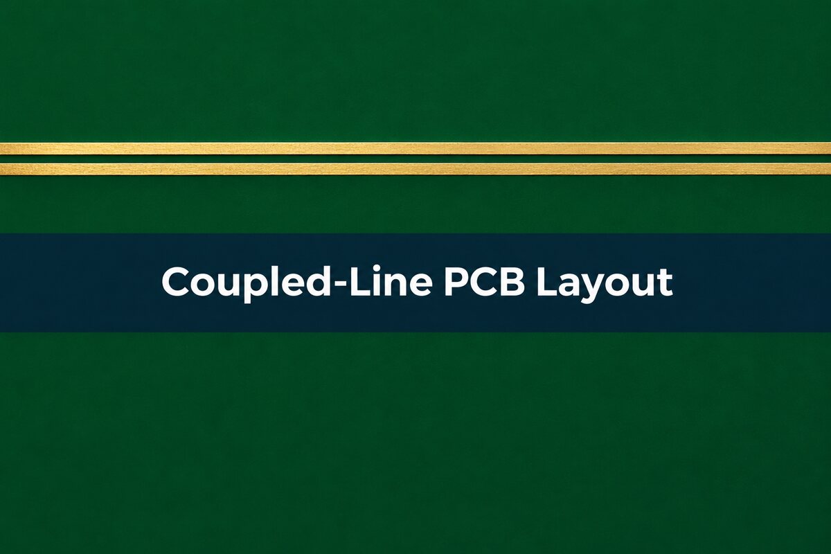
Microstrip is straightforward to inspect from the surface. A more symmetric stripline geometry can be worth evaluating when the isolated-channel floor limits performance, but it adds buried routing and launch transitions. A quarter guided wavelength is a starting point for some single-section designs, not a finished rule. Simulate the transitions, mask condition, line dimensions and expected manufacturing variation. See the Keysight RF design training note for coupled-mode design background.
Directional Coupler S Parameters: Lock the Port Map
Keep the physical port names beside the S-parameter file. An S term names the receiving port first and the driven port second. With the stated convention and unused ports terminated in the reference impedance, S21 is forward transmission, S31 is the desired forward sample, S41 is forward leakage into the reverse sample, and S42 is the desired reverse sample with P2 driven. Use measured reverse coupling rather than assuming it equals forward coupling.
For the reverse channel under this convention, the input-referenced rejection between equal incident waves on P1 and P2 is I41 − C42 in dB, where I41 = −20 log10|S41| and C42 = −20 log10|S42|. If you instead reference a reflection to the load beyond the through path, account for that through loss and state the measurement planes. This is why some instrument directivity calculations include a through term. Do not compare calculations made with different port maps or reference planes as if they were identical.
Directional Coupler VSWR Measurement: Set a Leakage Budget
Compare the wanted reverse sample with leakage from the forward path across the band. Assume +10 dBm forward at the coupler, negligible through loss for this teaching example, 25 dB load return loss and 20 dB reverse coupling. The wanted reverse sample is −35 dBm. A reverse channel with 30 dB rejection and 20 dB coupling leaks −40 dBm from the forward wave: only 5 dB below the wanted sample. At 40 dB rejection, the leakage is −50 dBm, 15 dB below.
The 10 dB improvement lowers the leakage power by a factor of ten. It does not mean the apparent reflected reading is always high: if the leak and reflection are coherent, phase can make them add or cancel. At a 5 dB power separation the leakage amplitude is about 56% of the wanted amplitude; at 15 dB it is about 18%. Use that difference to set a practical uncertainty or go/no-go margin based on the job. Neither 30 nor 40 dB is a universal acceptance limit.
Directional Coupler Directivity Measurement: Check the Fixture First
Before changing the PCB, rule out a bad reference plane, an unmatched unused port and a measurement limited by noise. Use a vector network analyzer (VNA) calibrated to the agreed plane. Terminate every unused port with a characterized load. Record the port map, sweep, through loss, loads, cables, calibration reference plane and any fixture removal method. The Keysight VNA measurement example documents a different port convention and shows why the fixture setup matters.
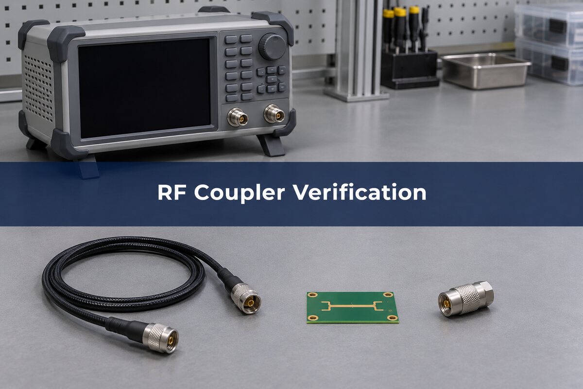
- Start with a matched load. Measure rejection and repeat after reconnecting or substituting an independently checked termination. If the curve changes materially, investigate the load or connection before reworking the layout.
- Check the useful floor. If a deep isolation trace jumps around near the instrument floor, make a repeat measurement with appropriate settings. State the lower bound you can support; do not report an exact isolation peak beyond the setup’s useful range.
- Separate board from fixture. If the error follows the cable or connector, fix that part and repeat. If the same error repeats on equivalent coupons after the test path checks pass, inspect the finished coupled gap, launches and terminations, and compare against the approved model.
Controlled Impedance PCB: What to Release for Fabrication
Release the finished stackup and coupling geometry together. A 50 Ω single-line coupon verifies an impedance target under its own conditions; it cannot qualify the coupling or isolation of the four-port circuit. If IPC-6018D (February 2022) is invoked on the order, specify the applicable performance class under §1.3.3 and confirm the relevant conductor width and spacing requirements in §§3.5.1.1–3.5.1.2. Those are board fabrication requirements, not the circuit’s coupling or directivity limits. Specify the RF limits and test setup separately.
Copyable RF release checklist: use it before making the first coupon or reviewing a supplier report. Fill each item from the drawing and test plan. Hold an acceptance conclusion when a missing item would change the measurement or its interpretation.
| Record | What to verify |
| RF target | Band, coupling and flatness, through loss, reverse-channel rejection, and reference planes. |
| Finished geometry | Material, pressed dielectric, finished copper dimensions, mask and actual measured gap. |
| Test evidence | Port map, calibration, loads, frequency traces, coupon revision, minimum result and evidence near the floor. |
| Worked decision row | Report shows 20 dB coupling but no P1-to-P4 leakage trace. Keep the coupling result; request leakage data before releasing reflected-power performance. |
PCB Directional Coupler FAQs
What is the difference between a 10 dB and a 20 dB coupler?
Under the same matched conditions, 10 dB coupling samples about 10% of incident power and 20 dB samples about 1%. Choose based on detector range and allowable main-line loading; the smaller attenuation value means stronger coupling, not necessarily better directivity.
Can I leave the unused coupled port open?
Not when you want the matched four-port response. An open reflects energy and can change the mounted response. Use the specified reference termination, often 50 Ω for an RF board, and confirm its return loss across the band. Follow the packaged component’s instructions if it has an internal termination.
Does 20 dB return loss mean 20% reflected power?
No. For a 20 dB return loss, reflected power is 1% of incident power at the same reference plane: 10−20/10. The reflection magnitude is 0.1, not 0.01. Keep the field-amplitude and power ratios separate when converting to VSWR.
Can I swap the forward and reflected sample connectors?
Reversing the driven direction can swap which port has the wanted sample, but port labels and internal loads vary. Confirm the connection map and required termination on the specific board. Recheck coupling and leakage in the new direction instead of assuming identical results.
Why does the circuit look correct at one frequency but fail near the band edge?
The wanted and unwanted components change amplitude and phase over frequency. A single point can hide the effect of launches, phase-velocity imbalance or terminations. Compare coupling, leakage and through loss over the full band; keep the same reference planes for both builds.
Can I copy a published line gap onto a different laminate?
Not directly. Specify the actual laminate, dielectric thickness, finished copper and mask before choosing width and gap. For a first prototype, review nominal and tolerance-corner model results, then measure the finished structure. A geometry from a different stackup is only a starting reference.
Does a power detector replace VNA characterization?
A detector is useful for the final monitoring circuit, but its gain, usable range and frequency response can obscure the coupler’s behavior. First characterize the passive paths with the reference terminations. Then verify the detector board with known input levels and loads.
Can I use a 75 Ω load on a 50 Ω PCB directional coupler?
Not as a matched load. For an ideal 75 Ω resistor at a 50 Ω reference plane, the reflection magnitude is |(75 − 50)/(75 + 50)| = 0.2, corresponding to about 14 dB return loss. Real adapters add frequency dependence. Use a characterized 50 Ω load over the measurement band instead.
Technical References
- Mini-Circuits: directional coupler terminology and termination effects.
- Keysight: VNA directional coupler directivity example.
- IPC-6018D: high-frequency board requirements, procurement and conductor geometry.
Need a Custom Directional Coupler PCB? Review the RF Stackup Before You Build
Keep an unverified gap or stackup from driving a second prototype. Best Technology’s controlled-impedance PCB service includes engineering stackup support, so you can discuss the dielectric and finished geometry before releasing the board. Ask about the impedance coupon option to check the reference-line target separately from the coupler’s four-port RF performance. Request a fabrication review and quote: send your Gerbers, stackup, finished trace and gap requirements, frequency band and target quantity to sales@bestpcbs.com.
You may also like

Tags: controlled impedance, Coupler Directivity, PCB Directional Coupler, RF PCB Design