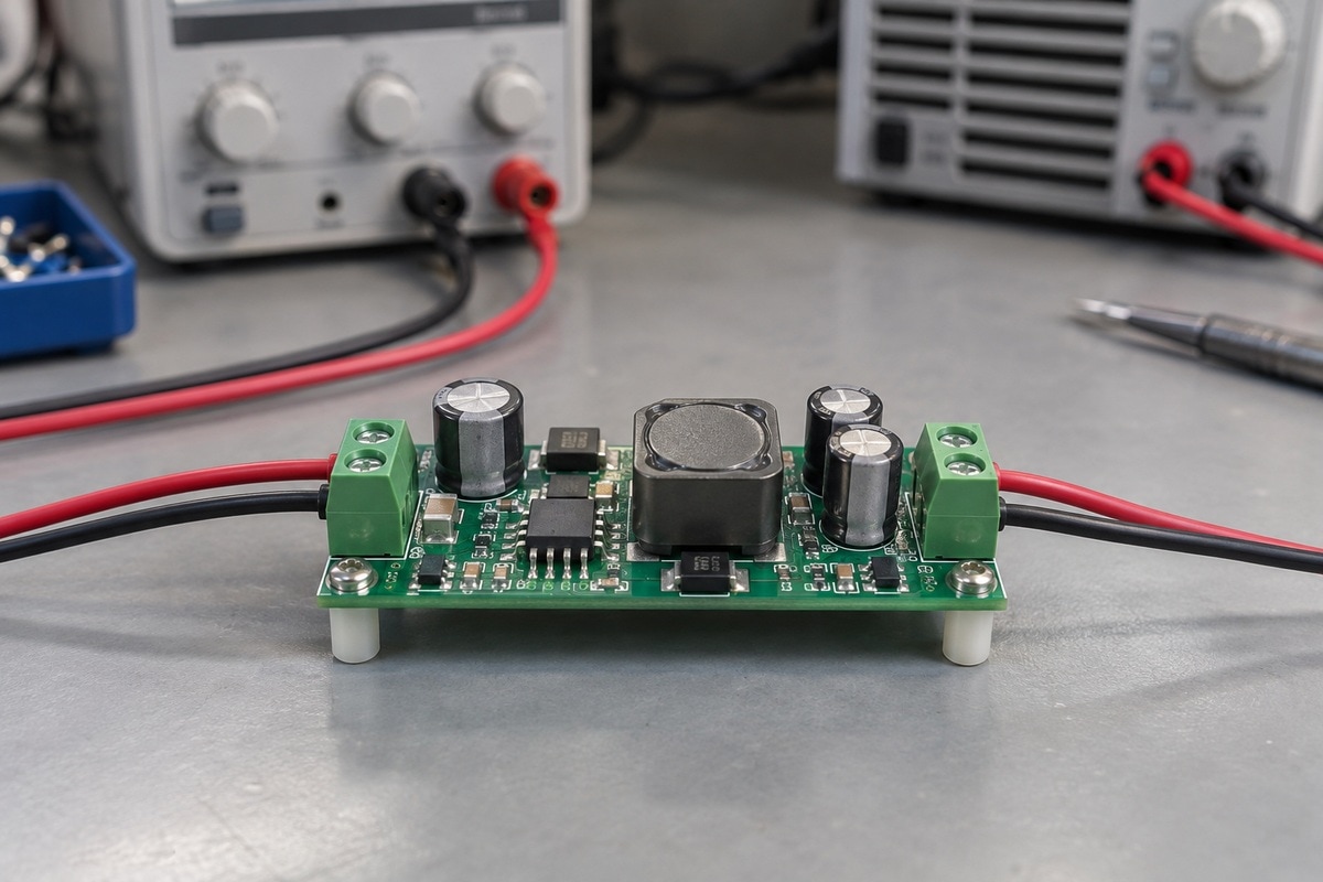
DC DC converter testing checks whether a power stage delivers the required voltage as its input, load, and operating temperature change. A correct reading at one operating point is only part of the picture. Startup waveforms, efficiency measurements, ripple, and load-step response show how the supply behaves when the conditions around it change.
EBest Circuit supports PCB fabrication, component assembly, and agreed functional testing for power electronics boards. Connecting assembly requirements with accessible test points helps make electrical checks practical on the finished PCBA. For a converter board prototype or production project, contact sales@bestpcbs.com to discuss manufacturing and test coverage.
What Equipment Is Needed for DC DC Converter Testing?
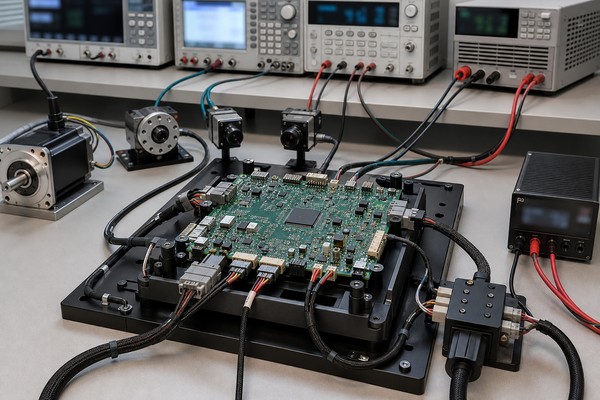
A typical bench uses a controllable DC source, an electronic load, voltage and current measurement, and an oscilloscope. Each instrument answers a different part of the performance question.
Equipment
Main use
Programmable DC supply
Apply input voltage and controlled input changes
Electronic load
Set output current and generate load steps
DMMs or a suitable power analyzer
Measure steady-state voltage, current, and power
Oscilloscope with suitable probes
Capture startup, ripple, and transient waveforms
Temperature sensors or thermal camera
Track heating during sustained operation
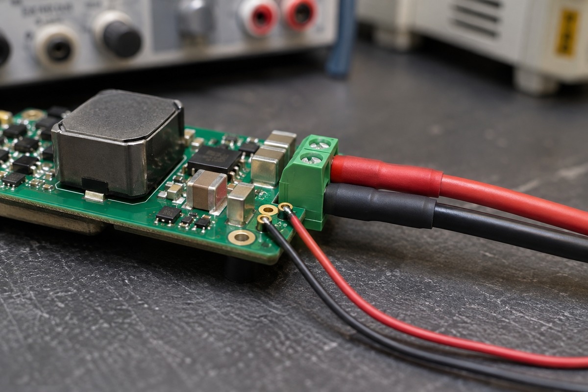
Connect the source to the converter input and the load to its output. Measure voltage at the board terminals: readings at the supply or load can include cable losses. Separate sense connections can improve accuracy where the equipment supports them.
The instrument ratings must cover the intended voltage, current, power, and transient conditions. For floating or isolated nodes, use a suitable differential or isolated measurement arrangement; an earth-referenced scope ground can unintentionally connect circuit nodes to earth.
How Do You Check Startup and Shutdown Behavior?
Capture input voltage and output voltage together to see when the converter starts, how its output rises, and what happens when power is removed. Include enable or power-good signals when those functions are present.
Apply the specified input transition. Start with the intended load connected and capture the complete output rise.
Measure the startup interval. Use the trigger and voltage thresholds defined for the product so repeated measurements are comparable.
Inspect the output peak. Compare overshoot and any interrupted rise with the permitted output limits.
Remove input power or disable the converter. Observe output decay and any required sequencing behavior.
Input power removal and an enable command are separate events. Output capacitance and the connected load can also change the shutdown waveform.
A board that repeatedly tries to start may be reaching its own protection limit, or the bench supply may be limiting current. Looking at the input waveform helps distinguish these possibilities before changing the converter circuit.
How Do You Measure Line and Load Regulation?
Line regulation describes output variation as input voltage changes. Load regulation describes output variation as output current changes. Vary one condition at a time to separate the two effects.
Test
Change
Keep fixed
Measure
Line regulation
Input voltage across the specified range
Output load
Settled output voltage at each input point
Load regulation
Output current across the specified range
Input voltage
Settled output voltage at each load point
Use the datasheet’s calculation convention when comparing results. Some specifications express variation in millivolts, others as a percentage or a change per unit of input voltage or current.
For example, an output spread from 4.98 V to 5.02 V is 40 mV, equivalent to 0.8% of a nominal 5 V output. That calculation alone does not establish a pass: the allowed range, reference value, and test conditions still determine acceptance.
Measure at the specified output point. A voltage drop at a distant load may include wiring resistance even when the converter’s terminal voltage remains stable.
How Do You Measure Converter Efficiency and Temperature Rise?
Efficiency compares power delivered with power taken in at the same operating point. For steady DC conditions with small ripple, the usual calculation is:
Use measurements at the converter terminals, with a clearly defined boundary for any auxiliary power. When voltage and current vary significantly, use a suitable instrument that averages instantaneous power rather than relying on the product of separate average readings.
Illustrative calculation. A board receiving 12 V at 0.95 A takes in 11.4 W. If it supplies 5 V at 2 A, it delivers 10 W. Its calculated efficiency is approximately 87.7%, with 1.4 W dissipated within the measured boundary.
Repeat measurements across the intended input and load range. A single peak-efficiency value does not describe light-load behavior or operation at another input voltage.
During sustained operation, record component temperatures together with ambient temperature, airflow, and mounting conditions. Temperature rise is the measured component temperature minus ambient temperature. Wait for the defined thermal steady-state condition before comparing results; a short power-on check does not reveal the final operating temperature.
How Do You Measure Output Ripple and Noise Accurately?
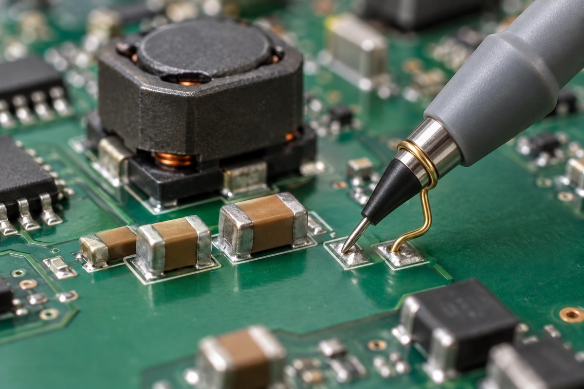
Probe connection and oscilloscope settings can materially change the observed waveform. A large probe loop may pick up switching interference and exaggerate the noise attributed to the output.
Use the specified measurement point. This is often across the output capacitor or designated output terminals.
Keep the measurement loop short. A ground spring or appropriate low-loop-area connection reduces pickup.
Match the specified bandwidth and coupling. A 20 MHz limit is common in some ripple measurements, but the product’s test method takes priority.
State the operating conditions. Record input voltage, output current, and any relevant operating mode alongside the peak-to-peak result.
Bandwidth-limited ripple and wider-band switching spikes are different measurements. Retain both where the application requires them, with the settings identified. A waveform captured under one bandwidth setting should not be compared directly with a limit defined under another.
For small signals, the probe and oscilloscope noise floor also matter. A reading close to that floor needs closer measurement review before it is attributed to the board.
What Does a Load Transient Test Reveal?
A load transient test shows how far output voltage moves and how quickly it recovers when current demand changes. It can expose behavior that steady-state regulation measurements miss.
Set the initial current, final current, transition speed, and dwell time to represent the intended load. Capture the actual current waveform as well as output voltage; a programmed load setting does not by itself confirm the step achieved at the board.
Waveform feature
Interpretation
Undershoot after a load increase
Output voltage falls while the converter responds to extra demand
Overshoot after a load decrease
Output voltage rises as the power stage adjusts to reduced demand
Settling time
Time taken to return to the specified voltage band
Ringing
A reason to investigate the control loop, input source, and interconnections
Ringing at the output does not identify its cause by itself. Observe the input rail too: input-supply resonance can appear in the output response. Load-step speed and wiring can also affect the result.
Use the application’s permitted voltage excursion and recovery time for acceptance. A transient test can reveal stability concerns, while a quantitative gain-and-phase assessment requires the appropriate loop-response measurement.
How Do You Test Overcurrent Protection and Fault Recovery?
Test the protection threshold and the recovery sequence together. A converter may limit current, restart periodically, or remain off until it receives a reset, depending on its design.
Begin within the normal operating range. Record input voltage, load current, and output voltage.
Apply the defined overload. Follow the product’s permitted current, duration, and test procedure using suitably rated equipment.
Observe the protection response. Capture the transition into current limiting or shutdown and any restart pulses.
Remove the overload. Verify automatic recovery or apply the specified reset, then repeat normal output measurements.
An overload test and a short-circuit test are not interchangeable. Short-circuit testing needs a controlled setup and a procedure appropriate to the converter’s rating.
Keep enough capability in the input source to avoid confusing its current limit with the converter’s protection. Where undervoltage lockout is specified, measure turn-off and restart thresholds separately; their difference describes the input-voltage hysteresis.
FAQs About DC DC Converter Testing
Can you test a DC DC converter with a multimeter?
A multimeter can check steady input and output voltage and, with the correct connection and rating, current. An oscilloscope is needed to examine fast events such as startup overshoot, switching ripple, and load-step response.
Is the correct no-load output voltage enough to pass a converter?
It establishes only the result at that condition. Performance under load, during transitions, and after heating requires additional measurements. Some converters also specify minimum-load conditions.
What belongs in a DC DC converter test plan?
Include input and load conditions, measurement points, instrument settings, temperature conditions, test timing, and acceptance limits. For dynamic tests, define the transition speed and the voltage band used to measure recovery.
How does production testing differ from design validation?
Design validation explores performance across the intended operating range and relevant corner conditions. Production testing uses an agreed set of repeatable checks to identify manufacturing defects and verify selected functions on assembled boards. Passing that set does not replace complete design validation.
Do isolated DC DC converters need additional tests?
Isolation requirements can add dielectric-withstand and insulation-resistance testing. Test voltage, duration, connections, and acceptance criteria depend on the product specification and applicable requirements; ordinary output measurements do not verify the isolation barrier.
Effective DC DC converter testing connects each measurement to a defined operating condition and an acceptance limit. For PCB fabrication, assembly, and agreed functional testing of your converter board, contact EBest Circuit at sales@bestpcbs.com to discuss a prototype or production build.
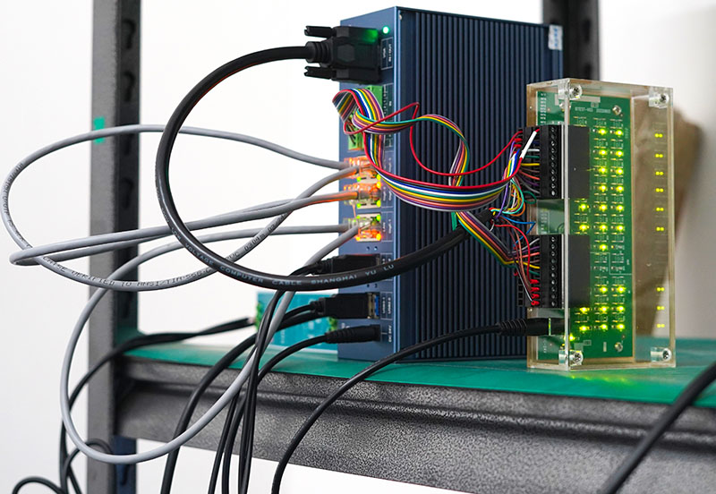
An AI robot testing PCB is a custom interface board used inside a fixture or automated station to connect a robot PCBA to measurement, programming, simulated sensors, communication loads, and controlled power. Its purpose is repeatability: every unit should see the same contacts, stimulus, sequence, limits, and result logging. A test PCB cannot compensate for missing test access, undefined limits, or an unstable product design, so test requirements must be developed with the unit under test before production tooling is released.
Are you worried about these problems in your AI robot testing PCB project?
Will inadequate test access leave hidden interconnect faults around dense packages and connectors?
Could an unstable fixture create false failures that slow production and conceal the real defect?
Will unclear limits produce test logs that cannot support release, repair, or traceability decisions?
Founded in 2006, EBest Circuit provides one-stop PCB and PCBA manufacturing support from engineering review and prototyping through assembly and production.
Coverage review: We map the supplied fault requirements to inspection, structural electrical checks, programming, and functional verification before fixture release.
Interface review: We check test pads, datum holes, connector access, fixture clearance, programming headers, and replaceable interface elements against the released CAD package.
Test-package review: We confirm power limits, loads, scripts, fixtures, golden-unit control, result fields, and acceptance criteria needed for quotation.
Ready to start your AI robot testing PCB project? Send the current test package to sales@bestpcbs.com.
What Is an AI Robot Testing PCB?
It is a purpose-built electrical interface between the robot PCBA and production test equipment. Depending on scope, it can route pogo-pin contacts, translate logic levels, switch loads, protect instruments, simulate sensors, break out communication buses, provide programming access, and identify the connected fixture revision. It is not the same as the robot controller under test, and it should not contain undocumented logic that changes the product’s acceptance behavior.
Bind the test PCB to its unit under test, station, and test stage. A fixture for bare-board continuity has different needs from an assembled-board ICT interface, a firmware-programming carrier, or a powered functional tester. Combining stages may reduce handling, but it can also increase fixture complexity and make fault isolation harder. Select the architecture from required coverage, production volume, cycle time, physical access, and repair workflow.
How Should Design for Test Be Planned on the Robot PCBA?
Design for test should start while test points, connectors, component spacing, and mechanical datums can still be changed. The product PCB needs accessible nodes for the defects and functions the test plan intends to detect. Test-pad diameter, pitch, solder-mask opening, spacing from components, probe direction, board support, and keep-out space affect whether contacts remain reliable across fixture wear and board variation.
Fault list: List the opens, shorts, wrong values, polarity errors, missing parts, solder faults, programming failures, interface faults, and functions that must be detected.
Access map: Assign a reachable pad, connector pin, scan cell, or functional observation for each required node and identify inaccessible nets.
Mechanical datum: Use stable locating holes or edges that relate the PCB to the fixture without loading fragile connectors or components.
Safe state: Document discharge, current limiting, actuator inhibition, and the conditions permitted before firmware is valid.
Service path: Preserve diagnostic access needed to reproduce a failed step outside the production station.
Which PCB Test Methods Belong in a Robot Production Line?
No single method proves every aspect of a robot PCBA, so coverage should be divided by defect type. AOI checks visible placement and solder features; X-ray may inspect hidden joints where required; flying probe or ICT detects many structural and component faults; boundary scan can reach supported digital interconnects with limited physical access; and functional test verifies powered behavior under defined stimulus. The chosen combination must state what each method detects and what it does not.
Method
Useful Coverage
Important Boundary
AOI or visual inspection
Presence, orientation, placement and visible solder conditions
Does not prove electrical function or hidden-joint integrity
Flying probe or ICT
Opens, shorts, values, polarity and accessible structural checks
Coverage depends on test access and circuit isolation
Boundary scan
Supported digital interconnects and device access
Requires compatible devices, scan-chain design and data
Programming
Device identity, firmware load and verification
Programming success does not prove product function
Functional test
Powered rails, interfaces, sensors, communications and outputs
May not isolate every assembly defect without structural tests
Use this matrix to prevent duplicated tests and uncovered faults. For example, a functional communication check may prove that one path works but may not isolate marginal solder joints on unused pins. Conversely, ICT can confirm connectivity without proving that the complete control loop behaves correctly.
How Are Test Pads and Probe Access Designed?
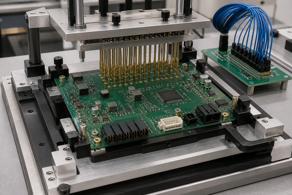
Test access should make stable contact without damaging the board or changing the circuit under test. Choose pads and probe types with the fixture supplier using the product stackup, finish, solder mask, expected cycles, contamination controls, and available force. Keep probes away from component bodies, solder fillets, moving connectors, board edges that flex, and high-speed nodes where added capacitance can change behavior.
Group power, ground, programming, and sensitive measurement contacts according to fixture needs. Provide adequate ground returns near fast or low-level signals, and avoid forcing large test currents through one small probe. If a connector is used instead of pogo pins, specify mating-cycle life, alignment, strain relief, replacement method, and how a partially seated condition is detected. The released test-point drawing must match the exact PCB revision and panel orientation.
Electrical loading: Record the maximum probe current, acceptable contact resistance, measurement bandwidth, and added capacitance permitted on each node so the fixture does not distort the result.
Contact geometry: Specify pad size, mask opening, finish, pitch, probe type, approach direction, and nearby keep-outs with the fixture supplier rather than leaving access to a generic test-point note.
Force and support: Add the total probe force and support locations to the mechanical review. A reachable pad can still produce intermittent contact or board strain when the probe field bows the assembly.
Maintenance access: Identify probes, connectors, and interface modules that technicians can inspect and replace without disturbing calibrated channels or changing the fixture datum.
How Should an AI Robot Testing PCB and Fixture Be Built?
A stable fixture controls alignment, probe force, board support, cable routing, electrical protection, and replaceable wear parts. The interface PCB should keep sensitive paths short, separate instrument protection from the product, and provide unmistakable keyed connections. Mechanical stops should prevent over-travel, while supports prevent bowing under the probe field.
Freeze the unit identity: Bind board revision, assembly variant, connector option, and permitted rework state to the fixture release.
Set datum and force: Locate the board from stable features, calculate probe force, and support areas that would otherwise flex.
Protect the station: Add appropriate current limiting, discharge, isolation, transient protection, and interlocks according to the hazards.
Control replaceable items: Record probe type, harness, interface PCB, relay, connector, and calibration or maintenance intervals.
Verify repeatability: Exercise multiple known units and repeated insertions, then investigate measurement spread before setting limits.
How Are Firmware Programming and Device Identity Controlled?
Programming should bind the correct image, configuration, security state, and verification result to the physical board identity. Record device part number, programming voltage, interface, clock, reset behavior, image hash or controlled revision, configuration words, calibration data, and readback method. If keys or credentials are involved, the test PCB and station must follow the product owner’s security process; secrets must not be embedded in uncontrolled fixture files.
Programming may occur before or during functional test. Earlier programming can support boundary scan or self-test, but a blank or partially programmed device needs a safe electrical state. Log the programmer, script and image revision with the board serial or lot, and distinguish successful data transfer from a verified boot and application-level self-check.
Pre-program checks: Verify target identity, supply and reset conditions, interface continuity, and the permitted blank-device state before enabling the programmer.
Controlled package: Release the firmware image, hash, programming script, configuration data, supported hardware revisions, and rollback policy as one controlled set.
Post-program evidence: Record write verification, configuration readback, device identity, security-state result, boot result, and any application self-test as separate fields so one success cannot conceal another failure.
Failure handling: Set the permitted erase or retry policy for a failed device, including the maximum number of attempts and the first-failure evidence that must be retained for diagnosis.
How Do You Power Up a Robot PCBA Safely During Test?
Use a staged, current-limited sequence that can stop before a wiring or assembly defect causes secondary damage. Begin with unpowered polarity, resistance, and isolation checks. Apply the approved source through measured protection, confirm primary rails, then enable downstream domains in the required order. Motors, heaters, solenoids, batteries, and other energetic loads should be inhibited or replaced by controlled loads until the board is ready for them.
The fixture specification should set the discharge time and require proof that dangerous or measurement-altering stored energy is removed before contact opens. Account for back-powering through communication pins, USB, programming headers, sensor supplies, and external equipment grounds. A shared bench ground can create a path that does not exist in the robot. Record source voltage, current limit, rail thresholds, sequence and abort conditions in the test specification.
How Are Robot Interfaces Functionally Tested?
Functional tests should apply representative stimulus and verify an observable response for each contracted interface. Communication buses need message, level, timing, termination, error and recovery checks appropriate to their protocol. Sensors may require calibrated stimuli or simulators. Motor and actuator outputs need controlled loads and safe observation of direction, enable, current feedback, fault reporting, and shutdown behavior.
Power and supervision: Verify rails, current draw, reset, watchdog, power-good and fault outputs under the defined station loads.
Digital communication: Exercise required CAN, Ethernet, USB, UART, SPI, I2C or other interfaces with controlled partners and error handling.
Sensor paths: Inject known electrical or physical stimuli and verify conversion, range, plausibility checks and reported status.
Actuator paths: Use safe loads or simulators to verify command, feedback, enable, direction and fault response without uncontrolled motion.
AI compute interface: Check boot prerequisites, high-speed link presence and supported diagnostics without treating an application boot as complete hardware coverage.
How Are Test Coverage, Limits, and False Failures Controlled?
Coverage must trace each required defect or function to a test step, while limits must separate acceptable product variation from fixture and measurement variation. A high pass rate is not proof of adequate coverage, and a tight limit is not useful when station uncertainty is comparable to the permitted range. Build a coverage matrix and perform measurement-system review before production release.
Build the coverage matrix: Give every required defect or function an owner method, accessible stimulus, observable result, numeric or categorical limit, and residual-risk entry. Mark an item uncovered when no independent observation exists; do not count a nearby measurement as coverage without a causal link.
Set limits from evidence: Start with the product requirement and expected component tolerance, then account for instrument accuracy, fixture resistance, contact variation, environmental range, software timing, and repeatability. Record who owns each limit and the data required before it may change.
Separate product and station variation: Repeat controlled units across insertions, fixture positions, stations, and relevant operating conditions. If the observed spread is too close to the acceptance window, improve the contact, method, or instrument path before tightening the product limit.
Challenge detection capability: Use controlled known-good, known-fault, and repeatability samples to prove that the station detects required failures and does not reject acceptable variation. Preserve the sample revision, known condition, usage history, and expected result.
Control retest: Save the first failing measurement before reseating or retrying. A retest policy should distinguish contact recovery, fixture maintenance, confirmed product repair, and an unexplained intermittent pass; unrestricted retry-until-pass behavior destroys diagnostic evidence.
When false failures rise, compare the same unit before and after probe cleaning or connector reseating, then repeat it on another fixture or channel when available. Correlate failures with probe count, relay channel, cable position, fixture temperature, software timestamp, supply waveform, and unit variant. Release evidence should include the coverage matrix, approved limits, repeatability results, known-fault challenge, residual-risk list, and controlled retest policy.
How Is an AI Robot Testing PCB Manufactured and Assembled for Validation?
The AI robot testing PCB must be manufactured and validated as part of the complete test station, not checked as an isolated interface board. Relay footprints, protection parts, high-cycle connectors, pogo interfaces, low-level analog paths, and high-current routes require controls matched to their electrical and mechanical duties. Release evidence must bind the interface board to its schematic, harness, fixture, scripts, limits, and supported unit-under-test revision.
Review the released data: Confirm the schematic, stackup, finished copper, surface finish, impedance requirements, drill and slot details, mechanical outline, connector orientation, assembly drawings, BOM, and approved substitutions. Resolve conflicts before tooling to prevent a PCB, fixture CAD, or harness revision mismatch.
Plan panelization and tooling: Set panel rails, fiducials, tooling holes, breakaway features, and board support without obstructing fixture datums, service connectors, or high-cycle contact areas. Confirm that depanelization will not distort the board or damage edge-mounted parts.
Fabricate and electrically test the bare boards: Produce the specified stackup and finish, inspect critical dimensions, and perform the agreed continuity and isolation test for opens and shorts. Controlled-impedance paths, high-current conductors, and fine-pitch features require their released acceptance criteria.
Assemble with component-specific controls: Verify polarity, connector keying, relay orientation, protection devices, replaceable parts, and soldering requirements for different thermal masses. Record the stencil, assembly program, approved component revisions, and manual operations to prevent incorrect placement or soldering.
Inspect workmanship and hidden joints: Use visual inspection and AOI for accessible features, with X-ray where the package or acceptance plan requires hidden-joint evidence. Check fixture mounting, connector seating, solder bridges, polarity, alignment, clearance, and each specified defect before applying power.
Verify every electrical channel: Measure continuity, isolation, channel resistance, switching state, leakage, protection behavior, and instrument paths against traceable limits. Exercise relays, multiplexers, translators, limited outputs, and replaceable channels so an untested path cannot cause a coverage failure or false pass.
Integrate the PCB with the fixture: Install the approved harnesses, probes, supports, interlocks, loads, and instruments. Confirm datum alignment, probe compression, board deflection, strain relief, grounding, discharge, and safe abort operation to prevent contact damage or unsafe fixture loading.
Qualify repeatability and release the station: Run repeated insertions with controlled known-good and known-fault samples, investigate measurement spread, and verify that required faults are detected without excessive false failures. Release the interface PCB, fixture, harness, software, limits, maintenance plan, and approved deviations as one controlled configuration.
What Files Are Needed for an AI Robot Testing PCB Quote?
A quotation needs both the interface-board manufacturing package and the product test definition. Supply Gerber or ODB++, drill and fabrication drawings, stackup, BOM, centroid and assembly drawings for the test PCB. Add the unit-under-test schematic, PCB data, test-point drawing, mechanical CAD, board variants, production volume, required cycle time, fault coverage, loads, programming package, communication specifications, limits, result fields, fixture concept and safety constraints.
Mechanical inputs: Unit outline, datums, component heights, keep-outs, probe side, connector access and permitted force.
Electrical inputs: Source limits, rail sequence, grounding, maximum probe current, interface levels, isolation and discharge requirements.
Data inputs: Firmware revision control, serial-number source, calibration data, test record schema, repair codes and retention rules.
Why Choose EBest Circuit for AI Robot Testing PCB Manufacturing?
EBest Circuit supports custom test-interface projects from design review and prototype assembly through controlled repeat production.
Free DFM and DFT review: We check PCB data, test access, fixture datums, connector clearances, wear parts, and assembly constraints early, helping you resolve manufacturability conflicts before tooling.
PCB and PCBA from one team: Coordinated fabrication, sourcing, assembly, and inspection reduce supplier handoffs and give your team one point for resolving data or component questions.
Prototype-to-production support: The approved board revision, BOM, substitutions, assembly files, and inspection requirements can remain controlled as volumes increase.
Build options matched to the interface: We can review multilayer, impedance-controlled, heavy-copper, high-Tg, and mixed-signal requirements against the actual fixture connections and loads.
Inspection matched to risk: The agreed bare-board electrical test, visual inspection, AOI, and applicable X-ray reduce the risk of discovering fabrication or soldering defects during fixture integration.
Quotation built around your test package: Send the unit-under-test data, coverage targets, fixture requirements, and quantities so we can confirm the PCB/PCBA scope clearly and avoid missing items after tooling begins.
FAQs About AI Robot Testing PCBs
Q1: Is an AI robot testing PCB the same as a load board?
A1:No; the boards have different primary functions. A testing PCB can route measurements, programming and simulated signals, while a load board is centered on presenting defined electrical loads. An interface PCB may include controlled loads, but each board should be named by function and have documented interfaces so the fixture cannot connect the wrong load or revision.
Q2: When is a bed-of-nails ICT fixture justified?
A2:Use dedicated ICT tooling when throughput and structural coverage justify its cost and maintenance. Low-volume or changing designs may favor flying probe or a simpler functional fixture. Compare test-point availability, fixture cost, maintenance, diagnostic value, throughput and expected design life before committing.
Q3: Can boundary scan replace physical test points?
A3:Only for supported digital interconnects; it cannot replace all physical access. Boundary scan requires compatible devices, a valid scan chain, accessible test access port and correct device data, and it does not cover every analog, power, passive or functional measurement. Build the coverage matrix by net and fault rather than applying a blanket replacement rule.
Q4: Should the fixture use a golden robot PCBA?
A4:Use a golden unit as a controlled station check, not as the only proof of test coverage. It can drift, wear or hide shared defects. Record its revision, known measurements, usage, storage, calibration relationship and replacement criteria. Use additional known-fault or diagnostic samples when needed to prove that required failures are detected.
Q5: How should pogo pins be maintained?
A5:Base inspection and replacement intervals on contact performance and cycle history. Account for probe type, finish, contamination, force and current, and monitor contact resistance and repeated-test behavior. Do not wait for obvious physical damage; intermittent contact can create false failures before a probe visibly breaks.
Q6: Can functional test prove all solder joints are good?
A6:No; a passing functional path does not prove every solder joint. An unused open pin, marginal joint, alternate current path or insufficient stress can remain undetected. Combine functional test with inspection, structural electrical test, boundary scan or X-ray according to the defects and package access. State residual risk for nets that remain unobserved.
Q7: How are multiple robot variants handled in one fixture?
A7:The station must identify and validate the variant before power or programming is applied. Use keyed connections, controlled adapters and separate limit sets. Record the unit variant, fixture adapter, software and limits with each result so data from one configuration cannot be accepted for another.
Q8: What is the difference between calibration and a golden-unit check?
A8:Calibration establishes measurement traceability; a golden-unit check verifies integrated station behavior. One does not replace the other. The quality plan should specify which channels require calibration, the applicable uncertainty, and how routine station checks are performed.
Q9: How should failed boards be diagnosed?
A9:Preserve the first failure and retest only under a controlled policy. Log the failing step, measured value, limit, fixture and software revision. Use structural diagnostics, schematics, boundary-scan logs, accessible nodes and substitute loads to isolate the cause. Unrestricted retesting until pass destroys useful evidence and can release intermittent defects.
Q10: What records should accompany production test?
A10:Each result must be traceable to the tested board, station, fixture, program, and limit revision. Record the timestamp, measured results, pass or fail disposition, repair action, retest history and operator or machine identity. Retention and data format should match the product quality plan and contractual requirements.
Conclusion
A repeatable robot PCBA test system begins with a fault list and test-access plan, then connects inspection, structural checks, programming and functional verification through controlled fixtures, limits and traceability. The test PCB is valuable only when its electrical and mechanical interfaces remain bound to the exact product and station revisions.
Send your Gerber/ODB++, BOM, unit-under-test data, test-point map, mechanical CAD, coverage matrix, fixture requirements, programming package, limits and result format to sales@bestpcbs.com for a free DFM review and AI robot testing PCB quotation.
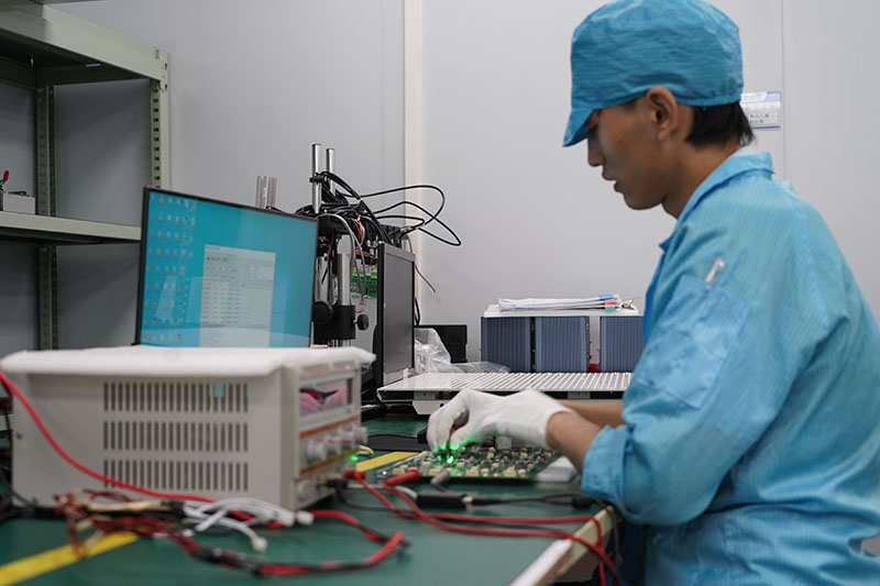
PCBA inspection is the cornerstone of electronics manufacturing, encompassing a suite of processes designed to verify the quality, functionality, and reliability of assembled printed circuit boards. This article explores the critical inspection methodologies that separate high-yield production from costly field failures.
What Are the Biggest Barriers to Consistent PCBA Quality?
Hidden defects: Solder bridges, insufficient solder, or BGA voids missed by visual checks
Rework & scrap: Late defect discovery drives repair and warranty costs
Supplier uncertainty: Limited visibility into a contract manufacturer’s real process control
Production delays: Manual inspection and testing slow output and launch timelines
No process feedback: Inspection finds errors but does not prevent repeat issues
How Can a Systematic Inspection Strategy Fix These Problems?
Multi-stage inspection: SPI, AOI, and AXI catch defects at the source
Process data control: Inspection data optimizes printing, placement, and reflow
Efficient test flow: Balanced optical, X-ray, and functional testing avoids bottlenecks
Closed-loop correction: Real-time feedback enables continuous process improvement
At EBest Circuit (Best Technology), we are a professional PCBA manufacturer committed to delivering high-quality and reliable PCB assemblies. Our investment in state-of-the-art PCBA inspection machines—from solder paste inspection (SPI) and automated optical inspection (AOI) to high-resolution X-ray systems—ensures every board meets the strictest standards. For a quote or to discuss your project’s inspection needs, contact us at sales@bestpcbs.com.
What Types Of PCBA Inspection Are Used In Modern Electronics Manufacturing?
Modern electronics manufacturing employs a layered inspection strategy, where different technologies are applied at various stages to form a comprehensive quality net. This multi-pronged approach is essential for catching a wide spectrum of PCBA defects.
Solder Paste Inspection (SPI): Applied immediately after stencil printing. A 3D laser scanner measures the volume, height, area, and alignment of deposited solder paste before component placement.
Automated Optical Inspection (AOI): Used post-reflow (and sometimes post-placement). High-resolution cameras capture 2D or 3D images of the assembled board to check for component presence, polarity, solder joint quality, and basic soldering defects.
X-Ray Inspection (AXI): Critical for inspecting hidden solder joints. It penetrates components to visualize connections under Ball Grid Arrays (BGAs), chip-scale packages, and within through-hole connectors, identifying voids, bridges, or misalignment.
In-Circuit Test (ICT): An electrical test that uses a bed-of-nails fixture to probe individual nets and components on the powered or unpowered board, checking for shorts, opens, resistance, and capacitance.
Flying Probe Test: A more flexible electrical test than ICT, using moving probes to access test points without a custom fixture, ideal for lower-volume or prototype runs.
PCBA Functional Testing: The final validation, where the assembled board is powered and operated in a simulated or real-world environment to verify it performs its intended function correctly.
From process verification (SPI) to structural analysis (AOI/AXI) and final electrical validation (ICT/Functional Test), this cascade of PCBA inspection services ensures defects are identified and corrected at the most cost-effective point in the assembly process.
How Does PCBA Solder Paste Inspection China Improve Assembly Yield?
Solder Paste Inspection (SPI) is the first and most critical automated checkpoint in PCBA production. Because solder paste quality directly determines solder joint reliability, effective SPI directly stabilizes and improves overall assembly yield.
By inspecting solder deposits before component placement, China PCBA solder paste inspection manufacturers prevent printing-related defects from flowing into placement and reflow, where correction becomes expensive and yield loss accelerates.
SPI links each measured parameter directly to a specific failure risk and yield outcome, allowing engineers to identify root causes quickly without overloading inspection data with interpretation.
How SPI Drives Real-Time Yield Improvement
SPI is not a final inspection gate. It is a process control tool.
When paste volume trends low or high, operators can immediately adjust stencil pressure, alignment, or cleaning frequency. Because errors are detected before components are placed or reflowed, SPI prevents unnecessary scrap, reduces rework loops, and protects expensive components.
Well-controlled SPI processes routinely reduce printing-related rework and scrap by up to 70%, delivering measurable first-pass yield gains.
Why SPI Is Essential for High-Reliability China PCBA
For any factory delivering high-quality China PCBA, a robust SPI process is non-negotiable. SPI controls the most fundamental variable in soldering: consistent and repeatable solder paste deposition.
Without SPI, downstream AOI, X-ray, or functional testing can only detect failures after value has already been added. With SPI, yield is protected at the earliest possible stage.
What Are The Most Common PCBA Defects Inspection Methods?
Effective PCBA defects inspection relies on matching the right technology to the failure mode. The most common methods form a complementary toolkit.
Visual Inspection (Manual & Automated):
Method: Human inspectors or AOI machines examine the board under light.
Catches: Component absence/misplacement, wrong polarity, visible solder bridges, lifted leads, excessive or insufficient solder (on visible joints), and marking errors.
Automated Optical Inspection (AOI):
Method: Cameras capture board images, which are compared to a “golden board” or programmed rules.
Catches: All visual defects at high speed and consistency. Advanced 3D AOI can also measure solder fillet shapes.
X-Ray Inspection (AXI):
Method: Uses X-rays to create an image based on material density.
Catches: PCBA defects hidden from view: voids in BGA solder balls, insufficient solder under chips, head-in-pillow defects, and alignment issues in QFNs or through-hole joints.
Electrical Testing (ICT & Flying Probe):
Method: Probes make physical contact with test points to measure electrical values.
Catches: Shorts (opens), incorrect component values (resistance, capacitance), missing or wrong components, and faulty diodes/transistors.
Functional Testing (FCT):
Method: The board is powered and interfaced with test fixtures/software to simulate real operation.
While an inspection camera for PCBA (AOI) excels at surface-level checks, a complete strategy requires X-ray for hidden joints and electrical tests for performance validation to ensure comprehensive coverage.
When Should You Use PCBA X Ray Inspection For BGA Assemblies?
PCBA X ray inspection is not always required, but it becomes essential for assemblies where solder joint integrity cannot be verified visually. Its use is dictated by component type, product criticality, and cost of failure.
You should mandate PCBA X Ray inspection for BGA assemblies in these scenarios:
High-Reliability Products: Medical, automotive, aerospace, or industrial control systems where failure is unacceptable.
Fine-Pitch or High-Density BGAs: Where solder ball pitch is below 0.8mm, increasing the risk of bridging and making alignment critical.
Mixed Technology Boards: Assemblies combining BGAs with through-hole or other complex components where thermal reflow is challenging.
First-Article Inspection & Process Validation: To qualify the stencil design, solder paste, and reflow profile for a new BGA component.
Failure Analysis & Root Cause Investigation: When a BGA-related fault is suspected, X-ray is the primary non-destructive tool for diagnosis.
Investing in high quality PCBA with BGA X-ray inspection is an insurance policy against latent defects. It provides undeniable proof of solder joint quality beneath the component, ensuring the structural integrity of the most critical connections on the board.
How Does A PCBA Inspection Machine Work In Mass Production?
In mass production, a PCBA inspection machine is a high-speed, automated system integrated into the assembly line. Its operation is a cycle of image capture, analysis, and action.
Programming: The machine is programmed with the board’s CAD data, creating a “golden” reference model of the correct assembly, including component placement, polarity, and solder joint criteria.
Board Handling: The conveyor automatically positions the board under the inspection system with precise fiducial alignment.
Image Acquisition: The system uses its sensors (lasers for SPI, cameras for AOI, X-ray emitter/detector for AXI) to scan the entire board, capturing detailed data points or images.
Image Processing & Analysis: Sophisticated software compares the captured data against the reference model. It analyzes thousands of features—paste volume, component presence, solder fillet shape, or joint integrity.
Defect Detection & Classification: The software flags any deviations beyond pre-set tolerances (e.g., “Paste Volume Error – Pad U5,” “Missing Component – R12,” “Solder Void >25% – BGA A1”).
Result Output & Action: The machine marks the board (e.g., with an ink dot) or sends a signal to the conveyor to route it to a repair or rework station. Simultaneously, it logs all data for Statistical Process Control (SPC), feeding information back to upstream machines (like the printer or placer) for automatic correction.
This automated, data-rich workflow is what makes wholesale offline optical PCBA inspection and in-line inspection viable for high-volume manufacturing, ensuring consistent quality without manual bottlenecks.
What Can An Inspection Camera For PCBA Reveal That AOI Cannot?
While AOI systems are the workhorse of PCBA inspection, a specialized inspection camera for PCBA—often referring to high-magnification manual or semi-automated microscopes—serves a different, vital role. It reveals details that standard in-line AOI is not designed to catch.
Micro-Scale Defects: Hairline cracks in components or substrates, subtle copper trace damage, or micro-scratches that are below the resolution or contrast threshold of a production-line AOI.
Material & Texture Issues: Solder discoloration (indicating contamination or thermal stress), flux residue quality, or inconsistencies in conformal coating or potting material.
3D Depth & Profile Analysis: While 3D AOI exists, a high-precision inspection camera with depth-from-focus or laser scanning can provide more detailed cross-sectional analysis of specific, complex solder joints.
Flexible & Non-Standard Angles: Inspecting the sides of tall components, inside connectors, or under overhangs on a flexible PCB assembly, which an overhead AOI camera cannot view.
Engineering Analysis & Debugging: When a functional test fails, engineers use these cameras to go pro to inspect PCBA areas manually, probe specific points, and diagnose root causes that automated systems may only flag as a general failure.
Think of AOI as the fast, comprehensive patrol officer catching obvious violations, while the specialized inspection camera is the detective examining the forensic details. Both are essential for a complete quality system.
What Does PCBA Functional Testing Verify Beyond Visual Inspection?
PCBA functional testing is the ultimate quality gate, moving beyond the “does it look right?” question of visual/optical inspection to answer “does it work right?”. It validates the assembled board as a complete electronic system.
Correct System Operation: Powers the board and verifies it boots, communicates, processes inputs, and delivers the correct outputs as per its design specifications.
Firmware & Software Integrity: Ensures the correct firmware is loaded and functions as intended, which no visual or X-ray inspection can assess.
Real-World Interface Performance: Tests all interfaces (USB, Ethernet, wireless, audio, display) under load to confirm they meet signal integrity and protocol standards (e.g., following specific USB PCBA inspection guidelines for signal quality).
Power Integrity & Thermal Performance: Measures current draw, voltage regulation under load, and can monitor for unexpected heating, identifying poor power delivery or shorted components that may pass a static optical check.
Timing & Synchronization: Validates that processors, memory, and peripherals interact with correct timing, catching issues related to clock signals or high-speed data paths.
While AOI can confirm a memory chip is present and well-soldered, only functional testing can prove it stores and retrieves data correctly. It is the final, critical step in assuring the reliability and performance promised by high-quality and reliable PCB assembly.
Why PCBA Inspection Must Be Built Into The Manufacturing Process?
Treating inspection as a separate, final audit is a costly and reactive strategy. PCBA inspection must be a built-in, integrated element of the manufacturing process to be truly effective for quality control.
Early Defect Detection = Lower Cost: Finding and fixing a solder paste error with SPI costs pennies. Finding a soldering defect after reflow costs dollars. Discovering it during functional test costs tens of dollars. Finding it in the field costs hundreds in reputation and warranty claims. In-line inspection pushes detection upstream.
Real-Time Process Control: Inspection data (SPI/AOI measurements) is fed back to printers and placers for automatic parameter adjustment. This creates a closed-loop, self-correcting production line that prevents defect generation, rather than just catching bad boards.
Data-Driven Continuous Improvement: Aggregated inspection data provides actionable SPC charts. Manufacturers can identify trends (e.g., one nozzle consistently misplaces parts) and perform root-cause analysis to permanently eliminate process flaws.
Ensures Traceability & Accountability: When each board is linked to its inspection data at every stage, full traceability is achieved. This is critical for industries with strict compliance requirements and for resolving any quality disputes.
Builds Confidence & Enables Scalability: A robust, embedded inspection framework provides undeniable proof of process capability. It gives brands confidence in their China PCBA solder paste inspection factory partner and allows for seamless, quality-consistent scaling of production.
Ultimately, integrated inspection transforms quality from a hoped-for outcome into a predictable, measurable, and controllable output of the manufacturing process itself.
PCBA inspection is the multi-faceted discipline that safeguards the functionality and longevity of every electronic device. From solder paste validation to X-ray analysis of hidden joints and final functional verification, a layered inspection strategy is non-negotiable for high-quality and reliable PCB assembly.
At EBest Circuit (Best Technology), our manufacturing philosophy is built on this principle. We integrate advanced SPI, AOI, and PCBA X-ray inspection technologies directly into our SMT lines, supported by comprehensive functional testing protocols. This commitment ensures we deliver assemblies you can trust, backed by transparent data and proven process control. For a technical discussion tailored to your specific application, contact our team at sales@bestpcbs.com.
FAQs
What’s the difference between PCB and PCBA?
A PCB (Printed Circuit Board) is the bare, unpopulated board with just the copper traces and laminate. PCBA (Printed Circuit Board Assembly) refers to the completed board after all electronic components (resistors, chips, connectors, etc.) have been soldered onto it.
What are the problems with PCBA?
Common PCBA defects include solder bridges (shorts), insufficient or missing solder (opens), misaligned or tombstoned components, wrong parts, reversed polarity, and solder voids—especially under BGA chips. Electrical issues like shorts and opens are also frequent problems.
What is PCBA used for?
PCBA is the foundational, functioning “brain” or “nervous system” of virtually every modern electronic device, from smartphones and laptops to medical equipment, automotive systems, and industrial controllers.
What is PCBA certification?
PCBA certification refers to compliance with industry quality and reliability standards. Common ones include ISO 9001 (Quality Management), IATF 16949 (Automotive), ISO 13485 (Medical Devices), and IPC-A-610 (Acceptability of Electronic Assemblies), which defines the workmanship criteria for soldering and assembly.
This website uses cookies to enhance your experience, remember your preferences, and help us understand how visitors use our site. You can accept all cookies, reject non-essential cookies, or manage your settings.
This website uses cookies to improve your experience while you navigate through the website. Out of these cookies, the cookies that are categorized as necessary are stored on your browser as they are essential for the working of basic functionalities of the website. We also use third-party cookies that help us analyze and understand how you use this website. These cookies will be stored in your browser only with your consent. You also have the option to opt-out of these cookies. But opting out of some of these cookies may have an effect on your browsing experience.
Necessary cookies are absolutely essential for the website to function properly. These cookies ensure basic functionalities and security features of the website, anonymously.
Cookie
Duration
Description
cookielawinfo-checkbox-analytics
11 months
This cookie is set by GDPR Cookie Consent plugin. The cookie is used to store the user consent for the cookies in the category "Analytics".
cookielawinfo-checkbox-functional
11 months
The cookie is set by GDPR cookie consent to record the user consent for the cookies in the category "Functional".
cookielawinfo-checkbox-necessary
11 months
This cookie is set by GDPR Cookie Consent plugin. The cookies is used to store the user consent for the cookies in the category "Necessary".
cookielawinfo-checkbox-others
11 months
This cookie is set by GDPR Cookie Consent plugin. The cookie is used to store the user consent for the cookies in the category "Other.
cookielawinfo-checkbox-performance
11 months
This cookie is set by GDPR Cookie Consent plugin. The cookie is used to store the user consent for the cookies in the category "Performance".
viewed_cookie_policy
11 months
The cookie is set by the GDPR Cookie Consent plugin and is used to store whether or not user has consented to the use of cookies. It does not store any personal data.
Functional cookies help to perform certain functionalities like sharing the content of the website on social media platforms, collect feedbacks, and other third-party features.
Performance cookies are used to understand and analyze the key performance indexes of the website which helps in delivering a better user experience for the visitors.
Analytical cookies are used to understand how visitors interact with the website. These cookies help provide information on metrics the number of visitors, bounce rate, traffic source, etc.
Advertisement cookies are used to provide visitors with relevant ads and marketing campaigns. These cookies track visitors across websites and collect information to provide customized ads.