An AI robot testing PCB is a custom interface board used inside a fixture or automated station to connect a robot PCBA to measurement, programming, simulated sensors, communication loads, and controlled power. Its purpose is repeatability: every unit should see the same contacts, stimulus, sequence, limits, and result logging. A test PCB cannot compensate for missing test access, undefined limits, or an unstable product design, so test requirements must be developed with the unit under test before production tooling is released.

Are you worried about these problems in your AI robot testing PCB project?
- Will inadequate test access leave hidden interconnect faults around dense packages and connectors?
- Could an unstable fixture create false failures that slow production and conceal the real defect?
- Will unclear limits produce test logs that cannot support release, repair, or traceability decisions?
Founded in 2006, EBest Circuit provides one-stop PCB and PCBA manufacturing support from engineering review and prototyping through assembly and production.
- Coverage review: We map the supplied fault requirements to inspection, structural electrical checks, programming, and functional verification before fixture release.
- Interface review: We check test pads, datum holes, connector access, fixture clearance, programming headers, and replaceable interface elements against the released CAD package.
- Test-package review: We confirm power limits, loads, scripts, fixtures, golden-unit control, result fields, and acceptance criteria needed for quotation.
Ready to start your AI robot testing PCB project? Send the current test package to sales@bestpcbs.com.
What Is an AI Robot Testing PCB?
It is a purpose-built electrical interface between the robot PCBA and production test equipment. Depending on scope, it can route pogo-pin contacts, translate logic levels, switch loads, protect instruments, simulate sensors, break out communication buses, provide programming access, and identify the connected fixture revision. It is not the same as the robot controller under test, and it should not contain undocumented logic that changes the product’s acceptance behavior.
Bind the test PCB to its unit under test, station, and test stage. A fixture for bare-board continuity has different needs from an assembled-board ICT interface, a firmware-programming carrier, or a powered functional tester. Combining stages may reduce handling, but it can also increase fixture complexity and make fault isolation harder. Select the architecture from required coverage, production volume, cycle time, physical access, and repair workflow.
How Should Design for Test Be Planned on the Robot PCBA?
Design for test should start while test points, connectors, component spacing, and mechanical datums can still be changed. The product PCB needs accessible nodes for the defects and functions the test plan intends to detect. Test-pad diameter, pitch, solder-mask opening, spacing from components, probe direction, board support, and keep-out space affect whether contacts remain reliable across fixture wear and board variation.
- Fault list: List the opens, shorts, wrong values, polarity errors, missing parts, solder faults, programming failures, interface faults, and functions that must be detected.
- Access map: Assign a reachable pad, connector pin, scan cell, or functional observation for each required node and identify inaccessible nets.
- Mechanical datum: Use stable locating holes or edges that relate the PCB to the fixture without loading fragile connectors or components.
- Safe state: Document discharge, current limiting, actuator inhibition, and the conditions permitted before firmware is valid.
- Service path: Preserve diagnostic access needed to reproduce a failed step outside the production station.
Which PCB Test Methods Belong in a Robot Production Line?
No single method proves every aspect of a robot PCBA, so coverage should be divided by defect type. AOI checks visible placement and solder features; X-ray may inspect hidden joints where required; flying probe or ICT detects many structural and component faults; boundary scan can reach supported digital interconnects with limited physical access; and functional test verifies powered behavior under defined stimulus. The chosen combination must state what each method detects and what it does not.
| Method | Useful Coverage | Important Boundary |
| AOI or visual inspection | Presence, orientation, placement and visible solder conditions | Does not prove electrical function or hidden-joint integrity |
| Flying probe or ICT | Opens, shorts, values, polarity and accessible structural checks | Coverage depends on test access and circuit isolation |
| Boundary scan | Supported digital interconnects and device access | Requires compatible devices, scan-chain design and data |
| Programming | Device identity, firmware load and verification | Programming success does not prove product function |
| Functional test | Powered rails, interfaces, sensors, communications and outputs | May not isolate every assembly defect without structural tests |
Use this matrix to prevent duplicated tests and uncovered faults. For example, a functional communication check may prove that one path works but may not isolate marginal solder joints on unused pins. Conversely, ICT can confirm connectivity without proving that the complete control loop behaves correctly.
How Are Test Pads and Probe Access Designed?
Test access should make stable contact without damaging the board or changing the circuit under test. Choose pads and probe types with the fixture supplier using the product stackup, finish, solder mask, expected cycles, contamination controls, and available force. Keep probes away from component bodies, solder fillets, moving connectors, board edges that flex, and high-speed nodes where added capacitance can change behavior.
Group power, ground, programming, and sensitive measurement contacts according to fixture needs. Provide adequate ground returns near fast or low-level signals, and avoid forcing large test currents through one small probe. If a connector is used instead of pogo pins, specify mating-cycle life, alignment, strain relief, replacement method, and how a partially seated condition is detected. The released test-point drawing must match the exact PCB revision and panel orientation.
- Electrical loading: Record the maximum probe current, acceptable contact resistance, measurement bandwidth, and added capacitance permitted on each node so the fixture does not distort the result.
- Contact geometry: Specify pad size, mask opening, finish, pitch, probe type, approach direction, and nearby keep-outs with the fixture supplier rather than leaving access to a generic test-point note.
- Force and support: Add the total probe force and support locations to the mechanical review. A reachable pad can still produce intermittent contact or board strain when the probe field bows the assembly.
- Maintenance access: Identify probes, connectors, and interface modules that technicians can inspect and replace without disturbing calibrated channels or changing the fixture datum.
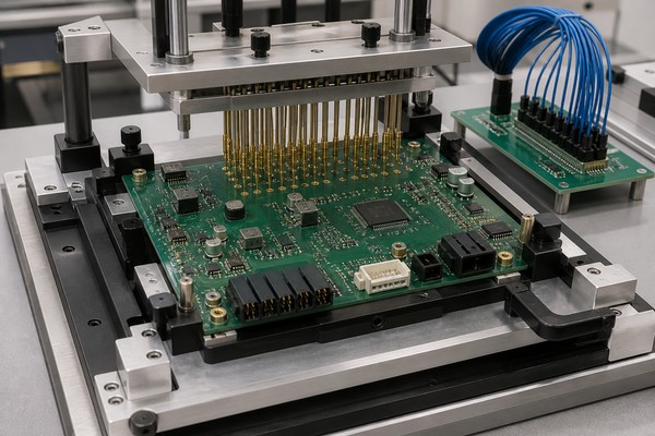
How Should an AI Robot Testing PCB and Fixture Be Built?
A stable fixture controls alignment, probe force, board support, cable routing, electrical protection, and replaceable wear parts. The interface PCB should keep sensitive paths short, separate instrument protection from the product, and provide unmistakable keyed connections. Mechanical stops should prevent over-travel, while supports prevent bowing under the probe field.
- Freeze the unit identity: Bind board revision, assembly variant, connector option, and permitted rework state to the fixture release.
- Set datum and force: Locate the board from stable features, calculate probe force, and support areas that would otherwise flex.
- Protect the station: Add appropriate current limiting, discharge, isolation, transient protection, and interlocks according to the hazards.
- Control replaceable items: Record probe type, harness, interface PCB, relay, connector, and calibration or maintenance intervals.
- Verify repeatability: Exercise multiple known units and repeated insertions, then investigate measurement spread before setting limits.
How Are Firmware Programming and Device Identity Controlled?
Programming should bind the correct image, configuration, security state, and verification result to the physical board identity. Record device part number, programming voltage, interface, clock, reset behavior, image hash or controlled revision, configuration words, calibration data, and readback method. If keys or credentials are involved, the test PCB and station must follow the product owner’s security process; secrets must not be embedded in uncontrolled fixture files.
Programming may occur before or during functional test. Earlier programming can support boundary scan or self-test, but a blank or partially programmed device needs a safe electrical state. Log the programmer, script and image revision with the board serial or lot, and distinguish successful data transfer from a verified boot and application-level self-check.
- Pre-program checks: Verify target identity, supply and reset conditions, interface continuity, and the permitted blank-device state before enabling the programmer.
- Controlled package: Release the firmware image, hash, programming script, configuration data, supported hardware revisions, and rollback policy as one controlled set.
- Post-program evidence: Record write verification, configuration readback, device identity, security-state result, boot result, and any application self-test as separate fields so one success cannot conceal another failure.
- Failure handling: Set the permitted erase or retry policy for a failed device, including the maximum number of attempts and the first-failure evidence that must be retained for diagnosis.
How Do You Power Up a Robot PCBA Safely During Test?
Use a staged, current-limited sequence that can stop before a wiring or assembly defect causes secondary damage. Begin with unpowered polarity, resistance, and isolation checks. Apply the approved source through measured protection, confirm primary rails, then enable downstream domains in the required order. Motors, heaters, solenoids, batteries, and other energetic loads should be inhibited or replaced by controlled loads until the board is ready for them.
The fixture specification should set the discharge time and require proof that dangerous or measurement-altering stored energy is removed before contact opens. Account for back-powering through communication pins, USB, programming headers, sensor supplies, and external equipment grounds. A shared bench ground can create a path that does not exist in the robot. Record source voltage, current limit, rail thresholds, sequence and abort conditions in the test specification.
How Are Robot Interfaces Functionally Tested?
Functional tests should apply representative stimulus and verify an observable response for each contracted interface. Communication buses need message, level, timing, termination, error and recovery checks appropriate to their protocol. Sensors may require calibrated stimuli or simulators. Motor and actuator outputs need controlled loads and safe observation of direction, enable, current feedback, fault reporting, and shutdown behavior.
- Power and supervision: Verify rails, current draw, reset, watchdog, power-good and fault outputs under the defined station loads.
- Digital communication: Exercise required CAN, Ethernet, USB, UART, SPI, I2C or other interfaces with controlled partners and error handling.
- Sensor paths: Inject known electrical or physical stimuli and verify conversion, range, plausibility checks and reported status.
- Actuator paths: Use safe loads or simulators to verify command, feedback, enable, direction and fault response without uncontrolled motion.
- AI compute interface: Check boot prerequisites, high-speed link presence and supported diagnostics without treating an application boot as complete hardware coverage.
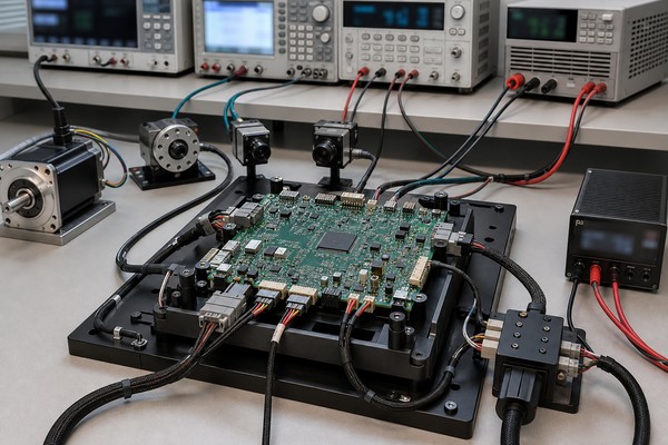
How Are Test Coverage, Limits, and False Failures Controlled?
Coverage must trace each required defect or function to a test step, while limits must separate acceptable product variation from fixture and measurement variation. A high pass rate is not proof of adequate coverage, and a tight limit is not useful when station uncertainty is comparable to the permitted range. Build a coverage matrix and perform measurement-system review before production release.
- Build the coverage matrix: Give every required defect or function an owner method, accessible stimulus, observable result, numeric or categorical limit, and residual-risk entry. Mark an item uncovered when no independent observation exists; do not count a nearby measurement as coverage without a causal link.
- Set limits from evidence: Start with the product requirement and expected component tolerance, then account for instrument accuracy, fixture resistance, contact variation, environmental range, software timing, and repeatability. Record who owns each limit and the data required before it may change.
- Separate product and station variation: Repeat controlled units across insertions, fixture positions, stations, and relevant operating conditions. If the observed spread is too close to the acceptance window, improve the contact, method, or instrument path before tightening the product limit.
- Challenge detection capability: Use controlled known-good, known-fault, and repeatability samples to prove that the station detects required failures and does not reject acceptable variation. Preserve the sample revision, known condition, usage history, and expected result.
- Control retest: Save the first failing measurement before reseating or retrying. A retest policy should distinguish contact recovery, fixture maintenance, confirmed product repair, and an unexplained intermittent pass; unrestricted retry-until-pass behavior destroys diagnostic evidence.
When false failures rise, compare the same unit before and after probe cleaning or connector reseating, then repeat it on another fixture or channel when available. Correlate failures with probe count, relay channel, cable position, fixture temperature, software timestamp, supply waveform, and unit variant. Release evidence should include the coverage matrix, approved limits, repeatability results, known-fault challenge, residual-risk list, and controlled retest policy.
How Is an AI Robot Testing PCB Manufactured and Assembled for Validation?
The AI robot testing PCB must be manufactured and validated as part of the complete test station, not checked as an isolated interface board. Relay footprints, protection parts, high-cycle connectors, pogo interfaces, low-level analog paths, and high-current routes require controls matched to their electrical and mechanical duties. Release evidence must bind the interface board to its schematic, harness, fixture, scripts, limits, and supported unit-under-test revision.
- Review the released data: Confirm the schematic, stackup, finished copper, surface finish, impedance requirements, drill and slot details, mechanical outline, connector orientation, assembly drawings, BOM, and approved substitutions. Resolve conflicts before tooling to prevent a PCB, fixture CAD, or harness revision mismatch.
- Plan panelization and tooling: Set panel rails, fiducials, tooling holes, breakaway features, and board support without obstructing fixture datums, service connectors, or high-cycle contact areas. Confirm that depanelization will not distort the board or damage edge-mounted parts.
- Fabricate and electrically test the bare boards: Produce the specified stackup and finish, inspect critical dimensions, and perform the agreed continuity and isolation test for opens and shorts. Controlled-impedance paths, high-current conductors, and fine-pitch features require their released acceptance criteria.
- Assemble with component-specific controls: Verify polarity, connector keying, relay orientation, protection devices, replaceable parts, and soldering requirements for different thermal masses. Record the stencil, assembly program, approved component revisions, and manual operations to prevent incorrect placement or soldering.
- Inspect workmanship and hidden joints: Use visual inspection and AOI for accessible features, with X-ray where the package or acceptance plan requires hidden-joint evidence. Check fixture mounting, connector seating, solder bridges, polarity, alignment, clearance, and each specified defect before applying power.
- Verify every electrical channel: Measure continuity, isolation, channel resistance, switching state, leakage, protection behavior, and instrument paths against traceable limits. Exercise relays, multiplexers, translators, limited outputs, and replaceable channels so an untested path cannot cause a coverage failure or false pass.
- Integrate the PCB with the fixture: Install the approved harnesses, probes, supports, interlocks, loads, and instruments. Confirm datum alignment, probe compression, board deflection, strain relief, grounding, discharge, and safe abort operation to prevent contact damage or unsafe fixture loading.
- Qualify repeatability and release the station: Run repeated insertions with controlled known-good and known-fault samples, investigate measurement spread, and verify that required faults are detected without excessive false failures. Release the interface PCB, fixture, harness, software, limits, maintenance plan, and approved deviations as one controlled configuration.
What Files Are Needed for an AI Robot Testing PCB Quote?
A quotation needs both the interface-board manufacturing package and the product test definition. Supply Gerber or ODB++, drill and fabrication drawings, stackup, BOM, centroid and assembly drawings for the test PCB. Add the unit-under-test schematic, PCB data, test-point drawing, mechanical CAD, board variants, production volume, required cycle time, fault coverage, loads, programming package, communication specifications, limits, result fields, fixture concept and safety constraints.
- Coverage inputs: Defect list, required functions, excluded functions, method ownership, and acceptance criteria.
- Mechanical inputs: Unit outline, datums, component heights, keep-outs, probe side, connector access and permitted force.
- Electrical inputs: Source limits, rail sequence, grounding, maximum probe current, interface levels, isolation and discharge requirements.
- Data inputs: Firmware revision control, serial-number source, calibration data, test record schema, repair codes and retention rules.
Why Choose EBest Circuit for AI Robot Testing PCB Manufacturing?
EBest Circuit supports custom test-interface projects from design review and prototype assembly through controlled repeat production.
- Free DFM and DFT review: We check PCB data, test access, fixture datums, connector clearances, wear parts, and assembly constraints early, helping you resolve manufacturability conflicts before tooling.
- PCB and PCBA from one team: Coordinated fabrication, sourcing, assembly, and inspection reduce supplier handoffs and give your team one point for resolving data or component questions.
- Prototype-to-production support: The approved board revision, BOM, substitutions, assembly files, and inspection requirements can remain controlled as volumes increase.
- Build options matched to the interface: We can review multilayer, impedance-controlled, heavy-copper, high-Tg, and mixed-signal requirements against the actual fixture connections and loads.
- Inspection matched to risk: The agreed bare-board electrical test, visual inspection, AOI, and applicable X-ray reduce the risk of discovering fabrication or soldering defects during fixture integration.
- Quotation built around your test package: Send the unit-under-test data, coverage targets, fixture requirements, and quantities so we can confirm the PCB/PCBA scope clearly and avoid missing items after tooling begins.
FAQs About AI Robot Testing PCBs
Q1: Is an AI robot testing PCB the same as a load board?
A1: No; the boards have different primary functions. A testing PCB can route measurements, programming and simulated signals, while a load board is centered on presenting defined electrical loads. An interface PCB may include controlled loads, but each board should be named by function and have documented interfaces so the fixture cannot connect the wrong load or revision.
Q2: When is a bed-of-nails ICT fixture justified?
A2: Use dedicated ICT tooling when throughput and structural coverage justify its cost and maintenance. Low-volume or changing designs may favor flying probe or a simpler functional fixture. Compare test-point availability, fixture cost, maintenance, diagnostic value, throughput and expected design life before committing.
Q3: Can boundary scan replace physical test points?
A3: Only for supported digital interconnects; it cannot replace all physical access. Boundary scan requires compatible devices, a valid scan chain, accessible test access port and correct device data, and it does not cover every analog, power, passive or functional measurement. Build the coverage matrix by net and fault rather than applying a blanket replacement rule.
Q4: Should the fixture use a golden robot PCBA?
A4: Use a golden unit as a controlled station check, not as the only proof of test coverage. It can drift, wear or hide shared defects. Record its revision, known measurements, usage, storage, calibration relationship and replacement criteria. Use additional known-fault or diagnostic samples when needed to prove that required failures are detected.
Q5: How should pogo pins be maintained?
A5: Base inspection and replacement intervals on contact performance and cycle history. Account for probe type, finish, contamination, force and current, and monitor contact resistance and repeated-test behavior. Do not wait for obvious physical damage; intermittent contact can create false failures before a probe visibly breaks.
Q6: Can functional test prove all solder joints are good?
A6: No; a passing functional path does not prove every solder joint. An unused open pin, marginal joint, alternate current path or insufficient stress can remain undetected. Combine functional test with inspection, structural electrical test, boundary scan or X-ray according to the defects and package access. State residual risk for nets that remain unobserved.
Q7: How are multiple robot variants handled in one fixture?
A7: The station must identify and validate the variant before power or programming is applied. Use keyed connections, controlled adapters and separate limit sets. Record the unit variant, fixture adapter, software and limits with each result so data from one configuration cannot be accepted for another.
Q8: What is the difference between calibration and a golden-unit check?
A8: Calibration establishes measurement traceability; a golden-unit check verifies integrated station behavior. One does not replace the other. The quality plan should specify which channels require calibration, the applicable uncertainty, and how routine station checks are performed.
Q9: How should failed boards be diagnosed?
A9: Preserve the first failure and retest only under a controlled policy. Log the failing step, measured value, limit, fixture and software revision. Use structural diagnostics, schematics, boundary-scan logs, accessible nodes and substitute loads to isolate the cause. Unrestricted retesting until pass destroys useful evidence and can release intermittent defects.
Q10: What records should accompany production test?
A10: Each result must be traceable to the tested board, station, fixture, program, and limit revision. Record the timestamp, measured results, pass or fail disposition, repair action, retest history and operator or machine identity. Retention and data format should match the product quality plan and contractual requirements.
Conclusion
A repeatable robot PCBA test system begins with a fault list and test-access plan, then connects inspection, structural checks, programming and functional verification through controlled fixtures, limits and traceability. The test PCB is valuable only when its electrical and mechanical interfaces remain bound to the exact product and station revisions.
Send your Gerber/ODB++, BOM, unit-under-test data, test-point map, mechanical CAD, coverage matrix, fixture requirements, programming package, limits and result format to sales@bestpcbs.com for a free DFM review and AI robot testing PCB quotation.
You may also like








Tags: PCBA Functional Testing, robot PCB design for test, robot PCB testing, robot testing fixture