If a TDR shows a dip near a PCB via, do not enlarge the antipad until you know the reflection really came from that transition. A launch can produce an overlapping event, and a short via can look like a single rounded dip rather than a separately measurable impedance section.
This guide follows an example 50 Ω channel from the reflection reading to a design decision. It shows how to tell a local impedance problem from a stub resonance or a fixture artifact, then define what a passing measurement actually looks like.
What Is PCB Via Impedance?
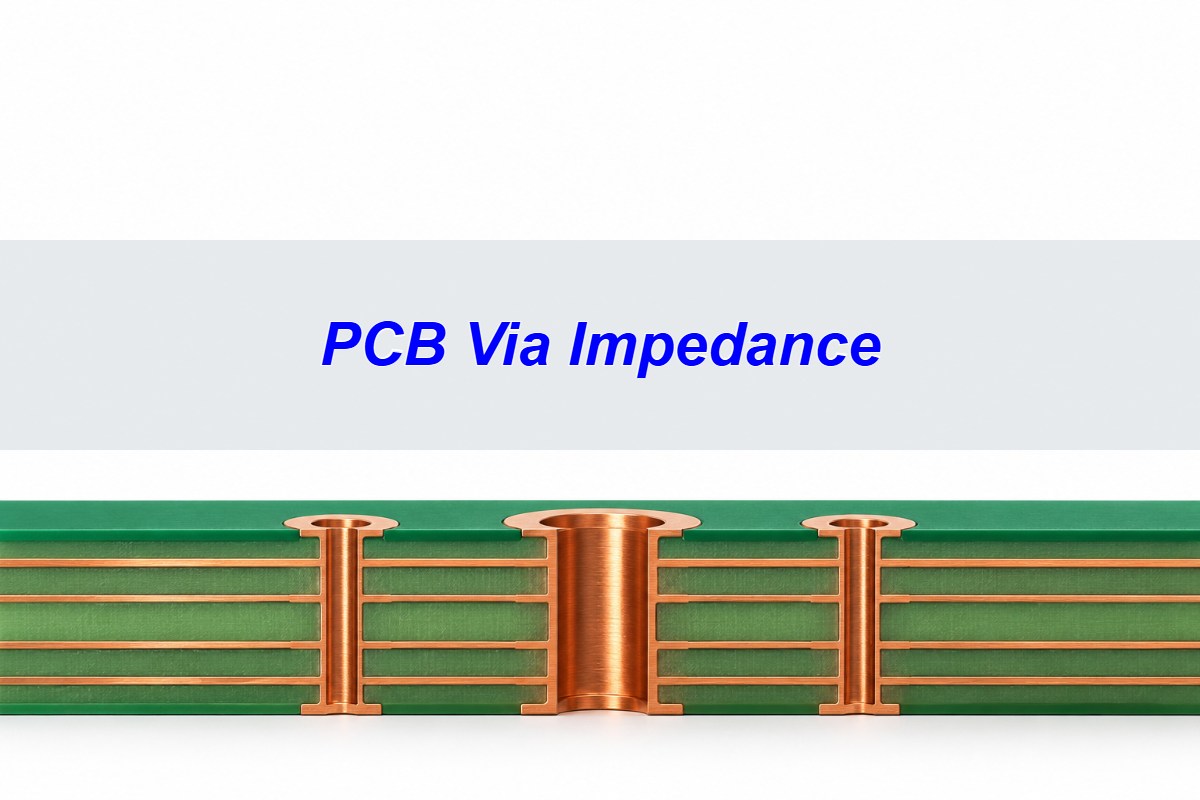
PCB via impedance describes how the layer transition presents itself to a traveling signal. It is not the DC resistance of the drilled barrel. The signal pad, barrel, clearances around it and the route taken by the return current all change the fields. This is why a trace that measures 50 Ω away from the transition can still have a reflection at the via.
For a coaxial connector feed, the goal may be a small local disturbance around a 50 Ω single-ended path. For a differential pair, assess the two vias as a coupled structure, including the pair’s return paths and symmetry. Do not compare a mixed-mode differential result with a 50 Ω single-ended target just because both ports of the instrument are individually 50 Ω.
PCB Via Antipad: What a Clearance Change Does
A small plane clearance can increase coupling to the plane and make the transition look more capacitive. Increasing the clearance may reduce that coupling, but an oversized void can also displace return current and make the transition look inductive. Check the net effect on the real stackup; a pad and an antipad are not independent controls.
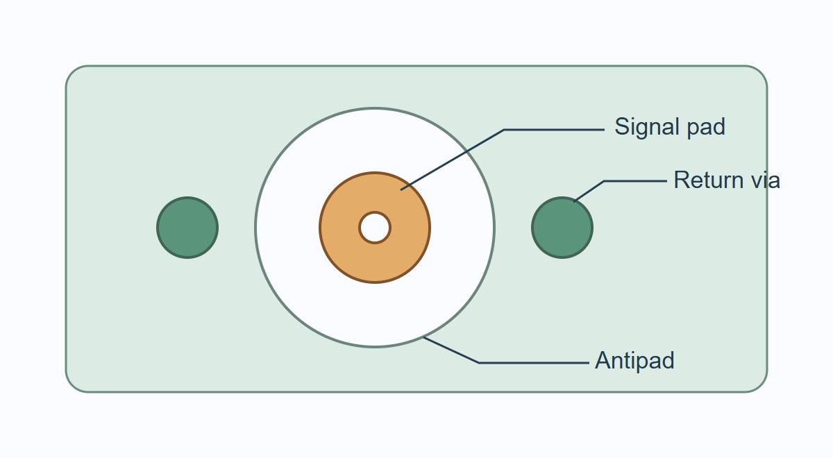
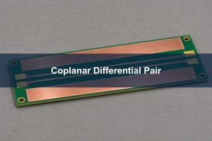
Record the finished hole, pad on every connected layer, plane openings, nonfunctional pads, and the start and destination layer. Keep the drill and registration limits from the fabricator in the model. For adjoining controlled-impedance traces, see the coplanar waveguide guide; a trace cross-section solution does not solve the three-dimensional via transition.
Return Path PCB Design for Layer Changes
When the old and new reference planes are the same ground net, nearby stitching vias can give current a shorter path between them. Place them with the signal transition in mind rather than adding random ground vias far from the change. For a differential pair, keep the return geometry and voids symmetric where practical and check for mode conversion as well as differential reflection.
When the references are different nets, do not short them to fix a TDR bump. Prefer a route that keeps a continuous reference if possible. If the design must change reference, model the intended AC return path and verify it over the signal bandwidth. At the bench, compare a geometry that keeps the same reference against the proposed layer change; compare the same launches, length and edge rate.
Via Stub Resonance vs a Local Impedance Event
A short local mismatch reflects part of the edge near the transition. An open-ended stub is an unused plated branch that can also create a frequency-dependent notch. The two effects can coexist. A small TDR dip alone does not prove that backdrilling will fix the link.
| Observed evidence | Check next | What would confirm it? |
| Short dip or peak tracks the via location | Pad, clearance and return geometry | Controlled candidate changes the event while a reference launch stays stable |
| Insertion-loss notch moves when stub length changes | Residual open branch and connected layer | Model and repeatable S-parameter measurements agree on the shift |
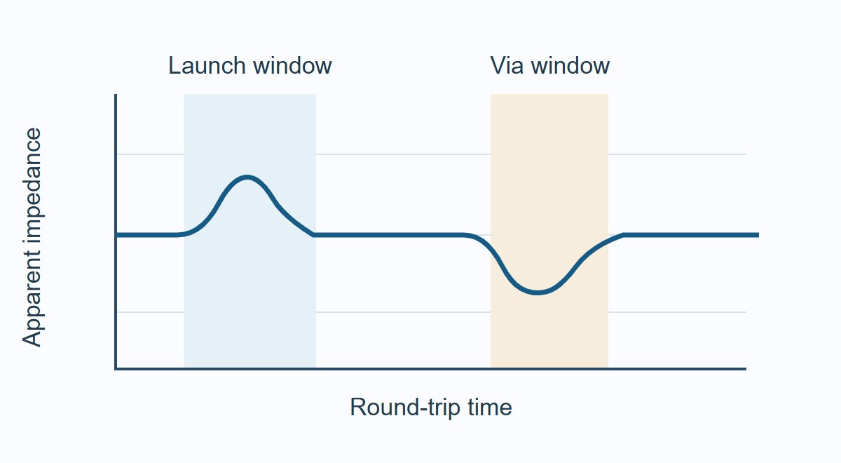
| Same event appears on a no-via reference | Launch, adapter, calibration and time-zero | Reference and device agree in the launch window, not at the intended via window |
A stackup with a short blind transition may avoid the unused branch, while a through hole with backdrilling can change fabrication and inspection cost. Use the separate via stub resonance guide for branch-length modeling; use the evidence above to decide whether it is the right issue to solve.
TDR Impedance Measurement: Set the Reference Plane
A TDR launches a fast edge and measures the returning wave. Set the measurement reference plane and record how launch and fixture effects are handled before reading impedance near the via. Use a matched termination where appropriate, verify a known line, and keep the launch and cable setup consistent across candidates.
Record the effective rise time at the device, not just the generator setting. In a simplified example with propagation speed 150 mm/ns, the round-trip time across 0.80 mm is about 10.7 ps. A 35 ps system edge corresponds to a round-trip one-way distance scale of about 2.6 mm at that speed. This is a scale comparison, not an instrument resolution guarantee; the 0.80 mm via may not produce a clean impedance plateau. Use a suited reference structure and cross-check in the frequency domain instead of treating the displayed dip as the exact barrel impedance.
Use a known-spacing TDR resolution check if the connector and via events overlap. The coupon can show whether your setup really separates the two reflections before you assign the dip to one feature.
TDR Impedance Plot: Turn a Reflection into a Checkable Result
Use the calibrated voltage reflection coefficient Γ. For reference impedance Zref, the impedance display uses Z = Zref(1 + Γ)/(1 − Γ). A −4% reflected-voltage step against a 50 Ω reference maps to 46.15 Ω. With +4% it maps to 54.17 Ω. The numbers are calculated examples; an isolated step and a composite peak are not the same physical evidence.
| Worksheet input | Worked example | Decision |
| Voltage reflection, referenced to the incident wave | Γ = −0.04; Zref = 50 Ω | Read a 46.15 Ω apparent event; compare at the same rise time |
| Round-trip time from calibrated origin; local velocity | 0.12 ns × 150 mm/ns ÷ 2 | Event near 9 mm along an assumed uniform path; check against physical layout |
| Same fixture and edge, no-via reference | Launch event present on both; later event on the via coupon | Send the later window to via analysis; do not retune the launch from it |
The distance calculation uses the local propagation velocity and a known time zero. Mixed stackups require measured or modeled delays along the actual route. The sign is a clue to capacitive or inductive behavior, not proof that any single feature caused it.
TDR Impedance Mismatch: Fix the Variable the Evidence Points To
Change one variable at a time and keep a control. If a confirmed local dip becomes smaller with the candidate clearance, test the wider band before approving it. If both candidates show a peak near the change of ground planes, model stitching and reference continuity first. If only the loss notch moves after shortening the stub, keep the more direct explanation rather than forcing the TDR minimum to explain it.
Use a field solver for the complete transition when point calculations or a single trace cannot resolve the cause. Include return vias, reference-plane boundaries, the landing traces and realistic manufacturing limits. Compare the measured model reference planes and use consistent edge speed or bandwidth for both candidates. If the lab fixture masks the event, redesign the coupon or improve fixture removal rather than accepting a reassuring number.
TDR Impedance Test: Define What Counts as a Pass
Agree on test ports, reference impedance, rise time, calibration and the time window in the release plan. A hypothetical RF design might accept an apparent 45–55 Ω in an isolated via window, then check its separate S11 limit over the specified frequency band. Under that assumed TDR criterion, 46.15 Ω would pass. It does not prove the rest of the RF path meets the return-loss limit.
For a high-speed serial differential transition, record the target differential reference and compare the mixed-mode return and insertion loss over the actual channel band. Confirm the eye or link margin if the end application requires it. For either use case, a straight-line impedance coupon may pass while the actual via transition fails; order a representative transition coupon if you need direct evidence. Ask for the files and plots with the measurement settings, trace markers and limits, not just a “passed” label.
If the supplier sends a straight-line coupon report, reconcile it with the drawing before using it as evidence for the uniform routes. This PCB impedance test report checklist shows how to separate a missing layer group from an out-of-limit measurement. Neither finding is evidence that the via transition itself passed.
PCB Via Impedance FAQs
Can I measure via impedance with a multimeter?
A multimeter can check continuity or resistance through the barrel, not the traveling-wave impedance. A TDR or a suitably configured network analyzer is needed to see high-frequency reflections.
Why does a larger antipad sometimes make the peak worse?
It reduces capacitive coupling but can also move the return current farther away. Check the complete return geometry and compare against the same connector and test fixture.
Can I use the same acceptance window for every rise time?
No. A faster edge can expose a disturbance that a slower edge averages out. Put the effective rise time and measurement plane in the specification.
Does a 50 Ω TDR display prove a 50 Ω via?
No. A short feature may be unresolved or masked by another event. An isolated plateau gives stronger evidence than a short rounded excursion, and both need fixture context.
What if the measured dip appears earlier than my layout estimate?
Check time-zero, cable skew, assumed velocity and the exact route length. Use the result from a known reference trace to reconcile the measurement plane with the layout.
Should ground vias be put inside the signal antipad?
Not as a default. They need intentional connection to the relevant ground planes and must not bridge the signal clearance. Verify the actual pad stack and keepout around the transition.
Can the same coupon qualify boards with different stackups?
Only if the tested structure still represents the relevant dielectric thicknesses, pads, references and fabrication tolerances. A coupon from a different construction does not automatically qualify the revised transition.
Is a TDR dip the same as a return-loss notch?
No. One is a time-domain feature; the other is frequency-dependent. Use the two views together, with the same fixture references, when the distinction affects the design.
Technical References
- Texas Instruments SLAAET6: antipad and return-via effects
- Texas Instruments SPRACP4A: via diameter, stubs and differential symmetry
- AMD XAPP1392: via impedance optimization
- Keysight: TDR and TDT concepts
Custom High-Speed PCBs with Engineering DFM Review
Need a high-speed board that can be built to your test plan? Send EBest Circuit the routed layers, proposed stackup, via and clearance dimensions, and the impedance or frequency-domain limits. Include the drawing for any representative transition coupon so the fabrication review covers the structure you actually intend to test.
Email sales@bestpcbs.com with the release files, quantity and acceptance requirements to request a quote and engineering DFM review.