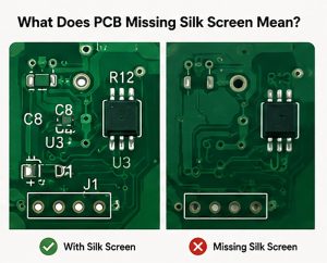
PCB missing silk screen means part or all of the printed legend layer is absent, unclear, clipped, misaligned, or unreadable on the finished circuit board. It may not always affect electrical function, but it can influence PCB assembly, polarity identification, inspection, traceability, and field maintenance.
What Does PCB Missing Silk Screen Mean?
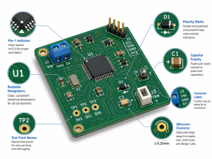
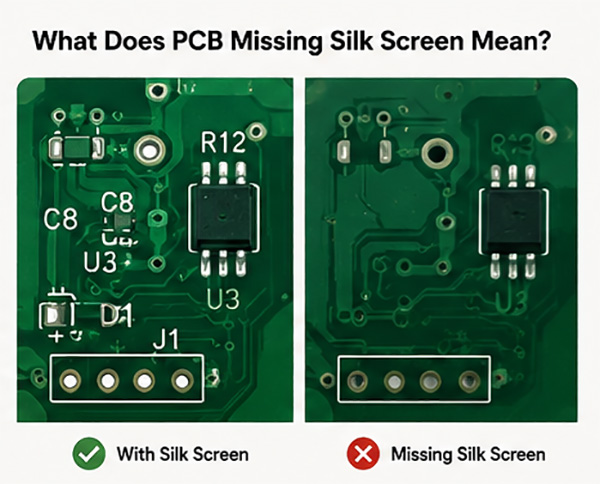
PCB missing silk screen means that the printed marking layer on the board is incomplete or not visible. This may include missing component reference designators, polarity marks, logos, pin-1 indicators, connector labels, test point names, warning marks, or revision codes.
In PCB manufacturing, the silk screen layer is also called the legend layer or nomenclature layer. It is usually printed in white, black, yellow, or another readable ink color on top of the solder mask. Its main role is not electrical conduction. Instead, it supports assembly, inspection, repair, traceability, and product identification.
A missing silkscreen on PCB does not always mean the circuit board is electrically defective. Many boards can still function normally without printed legend. However, for assembly, testing, field maintenance, regulated products, and high-mix production, missing silk screen can create practical risks.
Why Is Silk Screen Important on a PCB?
Silk screen is important because it turns a bare PCB into a readable manufacturing and service reference. It helps operators, inspectors, engineers, and end users understand the board layout quickly.
In PCB assembly, reference designators such as R12, C8, U3, D5, J1, and TP6 help operators match components to the correct locations. Polarity marks help identify the orientation of diodes, electrolytic capacitors, LEDs, ICs, connectors, and batteries. Test point names help engineers debug signals during functional testing.
| Silk Screen Information | Practical Use |
|---|---|
| Component reference designators | Helps assembly, inspection, and troubleshooting |
| Polarity marks | Prevents orientation errors for polarized parts |
| Pin-1 marks | Supports correct IC and connector placement |
| Test point labels | Speeds up electrical testing and repair |
| Revision code | Helps distinguish PCB versions |
| Logo and part number | Supports product identification |
| Warning marks | Improves safety for high-voltage or power boards |
| Connector labels | Helps cable installation and field maintenance |
Common Types of PCB Missing Silk Screen Problems
PCB missing silk screen can appear in several forms. Each type usually points to a different design, CAM, or manufacturing issue.
| Problem Type | What It Looks Like | Common Meaning |
|---|---|---|
| Entire silk screen missing | No text, logo, or marking on the board | Legend Gerber layer missing or not selected |
| Partial silk screen missing | Some labels visible, some absent | CAM clipping, solder mask conflict, or design issue |
| Text too faint | Legend exists but is hard to read | Ink thickness, curing, contrast, or surface issue |
| Misaligned silk screen | Text shifted from the correct position | Registration error during printing |
| Silk screen covered by components | Labels hidden after assembly | Layout placement issue |
| Silk screen printed on pads | Ink appears on exposed copper or solderable area | Poor DFM control or missing clearance |
| Broken characters | Text appears incomplete or fragmented | Line width too small or resolution limit |
| Missing polarity marks | Diode, LED, capacitor, or IC marks absent | Library or Gerber export error |
What Causes Missing Silk Screen on PCB?
PCB missing silk screen usually comes from design file issues, CAM processing, manufacturing capability limits, or production process control. The exact cause should be checked from Gerber data, fabrication notes, production records, and finished board inspection.
| Cause | Explanation | Prevention |
|---|---|---|
| Legend layer not included | The top or bottom silk screen file was not exported | Check the Gerber package before release |
| Wrong layer name | CAM may not identify the legend layer correctly | Use clear layer naming such as GTO and GBO |
| Silk screen overlaps pads | Manufacturer removes markings from solderable areas | Keep proper clearance from pads |
| Text line width too small | Fine text may disappear during printing | Follow minimum legend width rules |
| Text height too small | Tiny characters become unreadable | Use practical text size for production |
| Poor ink contrast | Ink color and solder mask color are too similar | Choose readable color combinations |
| Solder mask expansion issue | Legend is clipped by mask opening rules | Run DFM before fabrication |
| Printing registration error | Legend shifts during production | Control alignment and process tolerance |
| File conversion issue | DXF, ODB++, Gerber, or CAD export causes missing data | Review generated manufacturing files |
| Customer intentionally removed it | Some high-density or cosmetic boards omit silk screen | Confirm drawing and acceptance criteria |
Is Missing Silk Screen a Functional Defect?
Missing silk screen is usually not an electrical defect by itself. The copper circuits, solder mask, drilling, plating, impedance, and surface finish decide electrical performance. However, missing silk screen can become a manufacturing or quality risk when it affects assembly, inspection, test, traceability, or product use.
| Application Situation | Risk Level | Recommended Action |
|---|---|---|
| Simple prototype board | Low to medium | Confirm with engineer before use |
| Dense SMT assembly | Medium | Check assembly drawings and polarity marks |
| Power electronics | Medium to high | Verify warning marks and polarity |
| Medical electronics | High | Confirm traceability and documentation needs |
| Automotive electronics | High | Check revision control and inspection records |
| Aerospace or UAV boards | High | Review all markings and quality documents |
| Field-serviceable equipment | High | Ensure connectors and test points are readable |
How to Check PCB Missing Silk Screen Before Manufacturing
The best time to find missing silk screen is before PCB fabrication. Once boards are manufactured, correction becomes slower and more expensive.
Before releasing files, engineers should check the PCB legend layer in a Gerber viewer, not only in the PCB design software. CAD view and manufacturing output are not always identical.
| Check Item | What to Confirm |
|---|---|
| Top silk screen layer | GTO or top legend file is included |
| Bottom silk screen layer | GBO or bottom legend file is included if needed |
| Text visibility | Reference designators and marks are readable |
| Text height and width | Characters meet manufacturer capability |
| Pad clearance | Ink does not touch solder pads or exposed copper |
| Polarity marks | Diodes, LEDs, ICs, capacitors, and connectors are marked |
| Revision and part number | Correct PCB version is printed |
| Logo or customer marking | Included only if approved |
| Board outline relation | Text is not outside the final board edge |
| Assembly readability | Markings are still useful after components are mounted |
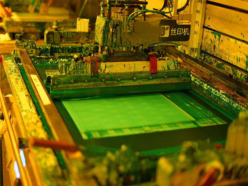
How Manufacturers Handle Silk Screen During PCB Fabrication
During PCB fabrication, the manufacturer reviews the legend layer during CAM processing. If silk screen overlaps pads, vias, solder mask openings, castellated holes, gold fingers, edge contacts, or test points, the CAM team may clip or remove those parts to protect solderability.
This is why some customers see missing silk screen even though the original design file included it. The legend may have been removed because it violated production rules.
| Manufacturing Step | Silk Screen Control Point |
|---|---|
| CAM review | Confirms legend layer, clearance, readability, and conflicts |
| Solder mask process | Defines openings where ink should not be printed |
| Legend printing | Applies ink by screen printing or inkjet printing |
| Curing | Hardens legend ink for adhesion and durability |
| Visual inspection | Checks readability, alignment, and missing areas |
| Final QC | Compares finished board with approved Gerber or drawing |
Can Missing Silk Screen Be Reworked?
Missing silk screen can sometimes be reworked, but feasibility depends on board type, quantity, required appearance, and acceptance standard.
For a small prototype batch, manual marking, label stickers, or controlled reprinting may be acceptable. For mass production or customer-facing products, rework must be handled carefully because uneven marking can affect appearance, traceability, and process consistency.
| Rework Method | Suitable For | Limitation |
|---|---|---|
| Manual marking | Engineering samples or internal prototypes | Not ideal for mass production |
| Adhesive labels | Box-build or internal identification | May not survive heat, solvents, or cleaning |
| Local reprint | Partial correction on selected areas | Requires process control and alignment |
| Full remake | Critical production boards | Higher cost but best consistency |
| Accept as-is | Non-critical missing legend | Requires written customer approval |
Design Rules to Prevent PCB Missing Silk Screen
Good legend design starts in the PCB layout stage. The goal is not to print every possible label. The goal is to print the right information in a readable and manufacturable way.
| Design Rule | Practical Recommendation |
|---|---|
| Keep text readable | Avoid extremely small characters |
| Use enough line width | Prevent broken or faint letters |
| Avoid pads and exposed copper | Keep legend away from solderable areas |
| Prioritize key marks | Keep polarity, pin-1, connector, and test point marks |
| Use clear orientation symbols | Mark diodes, LEDs, ICs, and electrolytic capacitors clearly |
| Avoid component body overlap | Place text where it remains visible after assembly |
| Confirm board side | Do not confuse top and bottom legend layers |
| Use consistent naming | Match BOM, assembly drawing, and PCB layout |
| Add revision marking | Support version control in production |
| Review final Gerber | Check output files, not only CAD layout |
How Missing Silk Screen Affects PCB Assembly
Missing silk screen can slow down PCB assembly because operators and inspectors need additional documents to confirm component placement. Automated SMT machines use centroid files, BOM, and programming data, so they do not rely only on legend. However, human inspection, first article inspection, repair, and debugging still benefit from clear markings.
| Assembly Stage | Possible Impact |
|---|---|
| Incoming board check | Harder to confirm board version |
| First article inspection | Slower component location verification |
| Manual component placement | Higher chance of orientation confusion |
| Through-hole assembly | Connector and polarity checks become slower |
| AOI review | Inspector may need more document cross-checking |
| Functional testing | Test point identification takes longer |
| Debug and repair | Engineers spend more time tracing circuits |
Industry Applications Where Silk Screen Quality Matters More
Some PCB applications can tolerate limited legend. Others need clear and stable board marking because production, maintenance, and compliance demands are higher.
| Industry | Why Silk Screen Matters |
|---|---|
| Industrial control | Helps identify terminals, relays, switches, and test points |
| Medical electronics | Supports traceability, inspection, and controlled production |
| Automotive electronics | Helps revision control and assembly verification |
| Aerospace and UAV | Supports documentation, reliability review, and maintenance |
| Communication equipment | Helps identify RF sections, connectors, and test points |
| LED lighting | Marks polarity, input/output direction, and thermal zones |
| Power electronics | Supports high-voltage warnings and connector identification |
| Consumer electronics | Improves product consistency and assembly communication |
Case Study: Solving Missing Silk Screen Before Batch PCB Production
In one production review scenario, a customer submitted a multilayer PCB design for industrial control equipment. The electrical data was complete, but the top legend layer had several clipped reference designators and missing polarity marks near small SMD diodes and connectors.
The problem came from two sources. First, several text labels were placed too close to solder mask openings. Second, some polarity marks used very fine line width, which was below the practical printing capability for stable production.
Before fabrication, the engineering review team corrected the issue by moving critical marks away from pads, enlarging polarity symbols, and keeping connector labels visible after assembly. Non-critical crowded reference designators were left to the assembly drawing instead of forcing unreadable text onto the PCB.
The result was a cleaner board layout, easier first article inspection, and lower risk during assembly. This kind of pre-production correction is often faster than discovering missing silk screen after boards arrive.
What Should Buyers Confirm Before Ordering PCBs?
Buyers should not treat silk screen as a small cosmetic detail only. For prototype and mass production orders, it is better to confirm legend requirements clearly before fabrication.
| Buyer Checkpoint | Why It Matters |
|---|---|
| Confirm whether silk screen is required | Some boards intentionally omit legend |
| Send complete Gerber files | Prevents missing top or bottom legend layers |
| Provide assembly drawing | Helps verify key markings |
| Specify ink color if needed | Improves readability and appearance |
| Confirm logo and part number | Avoids wrong branding or revision marking |
| Ask for DFM review | Finds pad overlap and unreadable text early |
| Request first article photos | Helps verify legend before full production |
| Define acceptance criteria | Avoids disputes over partial missing marks |
| Confirm controlled changes | Prevents CAM edits without approval |
| Keep revision records | Supports future repeat orders |
How to Choose a PCB Manufacturer for Better Silk Screen Control
A good PCB manufacturer should not only produce copper circuits correctly. It should also review practical manufacturing details such as legend readability, pad clearance, solder mask opening, version marking, and assembly support.
| Supplier Capability | Why It Helps |
|---|---|
| CAM engineering review | Catches missing or conflicting legend layers |
| DFM feedback | Helps fix issues before production |
| Prototype and mass production support | Keeps early samples and batch boards consistent |
| Visual inspection process | Finds faint, missing, or shifted markings |
| PCB and PCBA experience | Understands how legend affects assembly |
| Quality certifications | Supports controlled production systems |
| Engineering communication | Reduces file interpretation mistakes |
| Global delivery experience | Helps overseas buyers manage production schedules |
EBest Circuit (Best Technology) supports PCB design, PCB prototype, mass production, component sourcing, PCB assembly, and box-build assembly. With experience in FR4 PCB, multilayer PCB, MCPCB, ceramic PCB, flexible PCB, rigid-flex PCB, and high-frequency PCB production, the engineering team can help customers review silk screen risks before fabrication and assembly.
For projects requiring controlled documentation, EBest Circuit (Best Technology) can support quality-oriented production under systems such as ISO 9001, ISO 13485, IATF 16949, AS9100D, UL, RoHS, and REACH-related requirements, based on project scope and customer specifications.
FAQs About PCB Missing Silk Screen
What is PCB missing silk screen?
PCB missing silk screen means the printed legend layer is absent, incomplete, unreadable, or removed from the finished board. It may involve missing reference designators, polarity marks, connector labels, logos, test point names, or revision codes. The board may still work electrically, but assembly and inspection can become harder.
Is missing silk screen on PCB acceptable?
It depends on the project requirement. If the missing marking is cosmetic and the customer approves it, the board may be accepted. If polarity marks, safety labels, test point names, or revision codes are missing, the risk is higher. Production boards should be reviewed before acceptance.
Does silk screen affect PCB electrical performance?
Silk screen normally does not affect circuit conductivity because it is not part of the copper circuit. However, if legend ink is printed on pads or solderable surfaces, it may affect soldering quality. Missing silk screen can also affect assembly accuracy and troubleshooting efficiency.
Why did my PCB manufacturer remove part of the silk screen?
Manufacturers often remove or clip silk screen when it overlaps solder pads, vias, exposed copper, gold fingers, edge connectors, or solder mask openings. This is usually done to protect solderability. A proper DFM review should identify these conflicts before production starts.
Can silk screen be printed over solder pads?
Silk screen should not be printed over solder pads. Ink on pads may interfere with solder wetting and create assembly defects. Good PCB design keeps legend away from solderable areas, especially around fine-pitch ICs, connectors, test points, and small passive components.
What is the difference between silk screen and solder mask?
Solder mask is the protective coating that covers copper areas and helps prevent solder bridging. Silk screen is the printed text, symbols, and markings placed on top of the solder mask. Solder mask supports electrical insulation and soldering control, while silk screen supports identification and assembly.
What files control the PCB silk screen layer?
In Gerber data, the top silk screen layer is often named GTO, and the bottom silk screen layer is often named GBO. File naming may vary by CAD software. Buyers should check the final Gerber output in a viewer before sending files to the manufacturer.
Why is only part of my silk screen missing?
Partial missing silk screen is often caused by pad overlap, small text size, thin line width, CAM clipping, solder mask clearance rules, or printing registration limits. The best way to identify the cause is to compare the original Gerber layer with the manufacturer’s CAM output and finished board photos.
Can missing silk screen be fixed after PCB fabrication?
Sometimes it can be fixed through manual marking, labels, local reprinting, or remake. The right method depends on board quantity, product requirement, appearance standard, and risk level. For critical polarity, safety, or traceability markings, a controlled correction is usually needed.
How small can PCB silk screen text be?
The practical minimum text size depends on the manufacturer’s process, ink type, printing method, solder mask color, and inspection standard. Very small text may break, blur, or disappear. For reliable production, engineers should confirm minimum text height and line width with the PCB supplier before fabrication.
What color is best for PCB silk screen?
White silk screen on green solder mask is the most common choice. White also works on black, blue, red, and purple solder mask, but process control affects readability. For white solder mask, black legend is often preferred because it gives better contrast.
Should all components have silk screen reference designators?
Not always. On dense boards, printing every reference designator may create clutter or unreadable text. Critical information should be prioritized, including polarity marks, pin-1 indicators, connector labels, test points, warning labels, and board revision codes. The full reference designators can also be shown in the assembly drawing.
How can I prevent missing silk screen in mass production?
Check the Gerber files, confirm the legend layer, keep proper clearance from pads, use readable text size, review polarity marks, and request DFM feedback before production. For important projects, ask for first article photos or sample approval before full batch manufacturing.
Is silk screen needed for PCB assembly?
SMT machines use placement data, BOM, and machine programs, so silk screen is not the only source for assembly. Still, it helps operators, inspectors, and engineers during first article inspection, manual insertion, debugging, repair, and test point identification. It is especially useful for mixed SMT and through-hole assemblies.
What should I do if I receive PCBs with missing silk screen?
First, compare the finished board with the approved Gerber files and fabrication drawing. Then check whether the missing marks affect assembly, polarity, safety, inspection, or traceability. If the risk is low, written acceptance may be possible. If the risk is high, request correction, remake, or engineering review.
Conclusion
PCB missing silk screen is often a small-looking issue with real manufacturing consequences. It may not damage electrical performance directly, but it can affect assembly accuracy, inspection speed, test efficiency, product identification, and long-term maintenance. The best solution is early prevention: review Gerber files, confirm legend layers, keep markings away from pads, and ask for DFM feedback before production.
For engineers, the main selection advice is clear: prioritize readable polarity marks, connector labels, test point names, safety markings, and revision control over crowded cosmetic labeling. For buyers, the most practical procurement step is to work with a PCB manufacturer that checks both fabrication quality and assembly usability.
If you need support for PCB missing silk screen review, custom PCB fabrication, PCB prototype, mass production, OEM manufacturing, ODM production, sample development, or custom engineering solutions, EBest Circuit (Best Technology) can help review your files and provide practical manufacturing advice.
If you’re sourcing reliable PCB/PCBA manufacturing — OEM, ODM, prototyping, mass production, or custom engineering solutions — reach out to our engineering team for technical support and a quote at sales@bestpcbs.com.